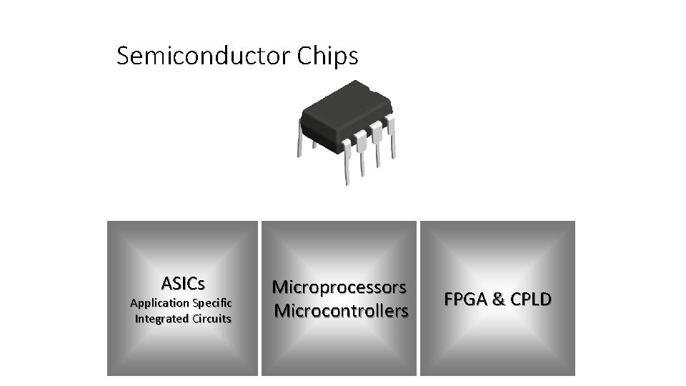
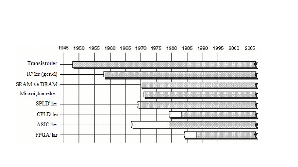
Semiconductor Chips ASICs Application Specific Integrated Circuits Microprocessors

![FPGAs…. [1] Company General Architecture Logic Block Type Programming Technology Xilinx Symmetrical Array Look-up FPGAs…. [1] Company General Architecture Logic Block Type Programming Technology Xilinx Symmetrical Array Look-up](https://slidetodoc.com/presentation_image_h/cb496402b2c1d04aff7fa784f2296b11/image-9.jpg)

![Lookup Tables used as memory (16 x 2) [ Distributed Memory ] Xilinx FPGAs Lookup Tables used as memory (16 x 2) [ Distributed Memory ] Xilinx FPGAs](https://slidetodoc.com/presentation_image_h/cb496402b2c1d04aff7fa784f2296b11/image-50.jpg)


- Slides: 95

Semiconductor Chips ASICs Application Specific Integrated Circuits Microprocessors Microcontrollers FPGA & CPLD

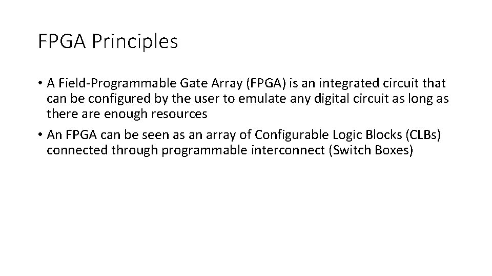
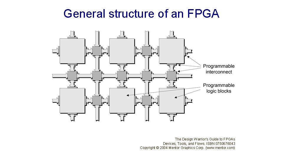
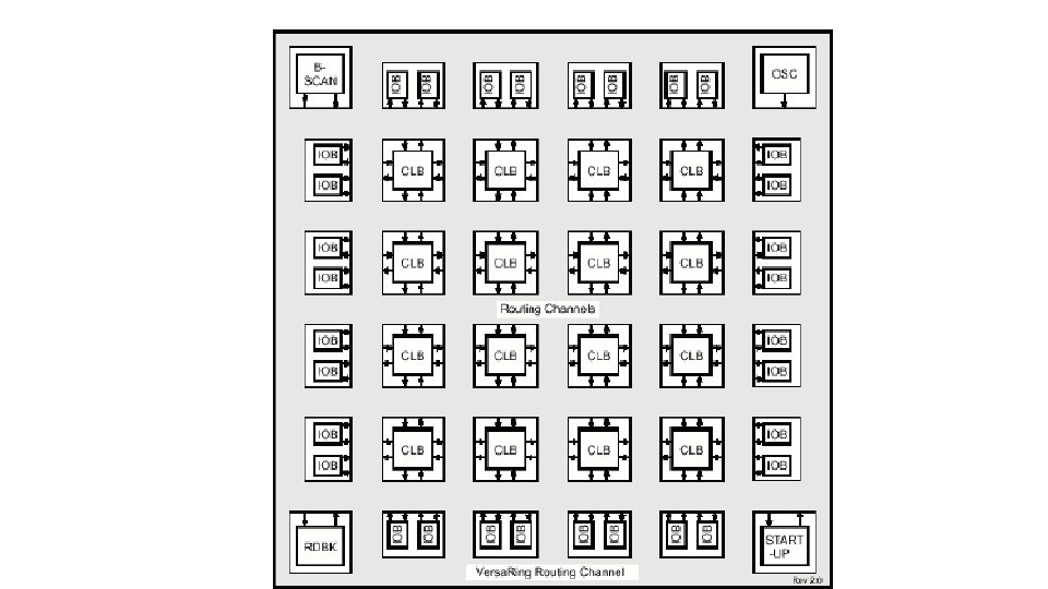
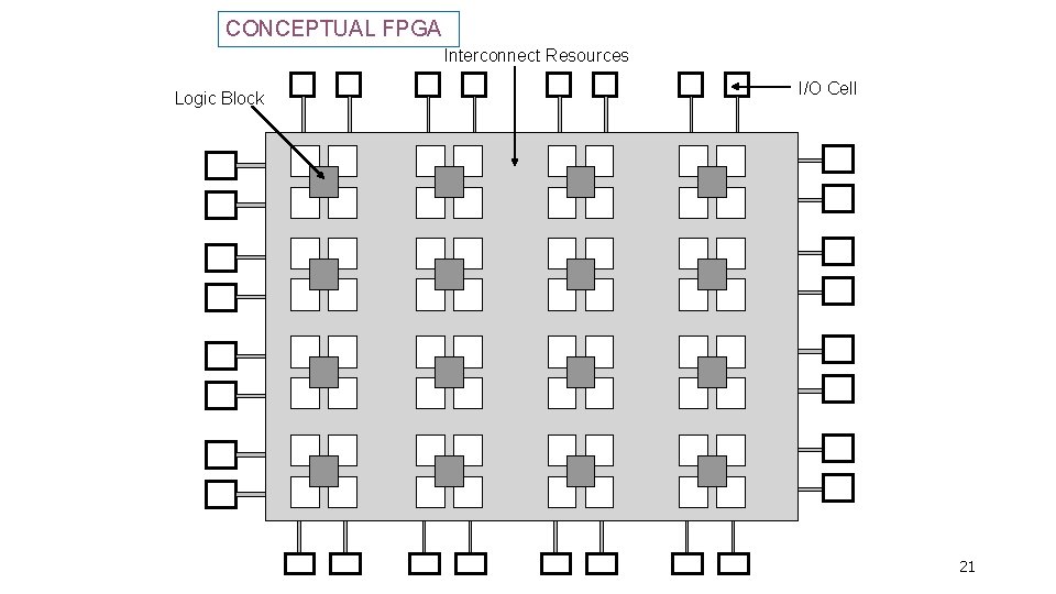
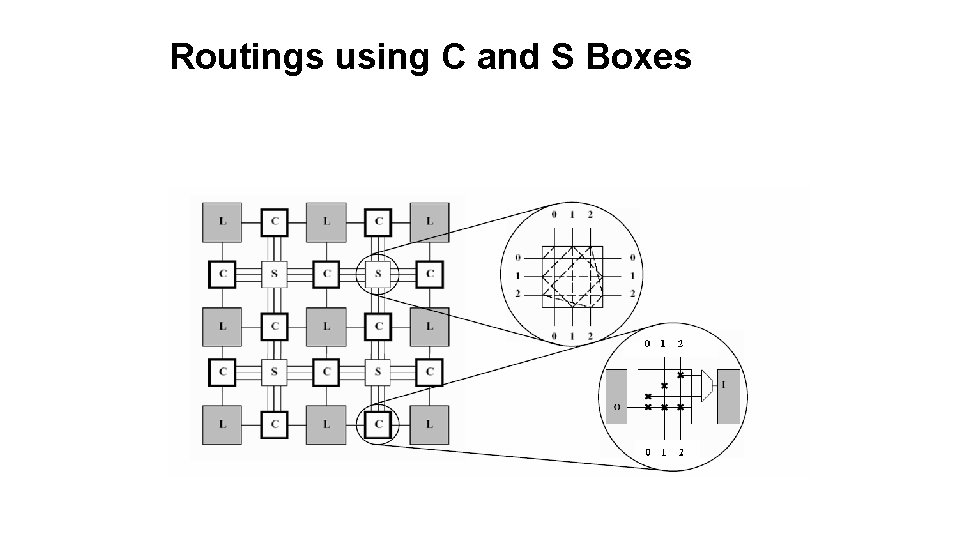
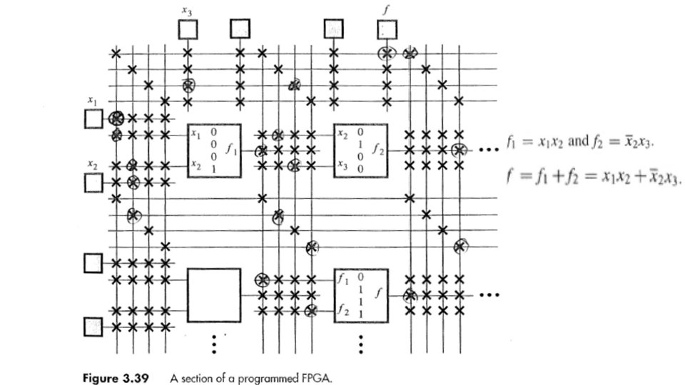
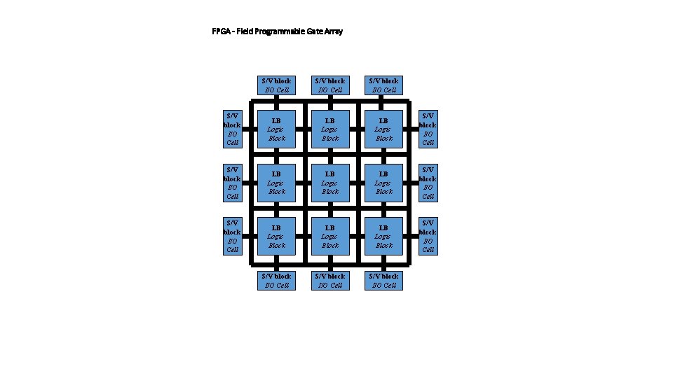
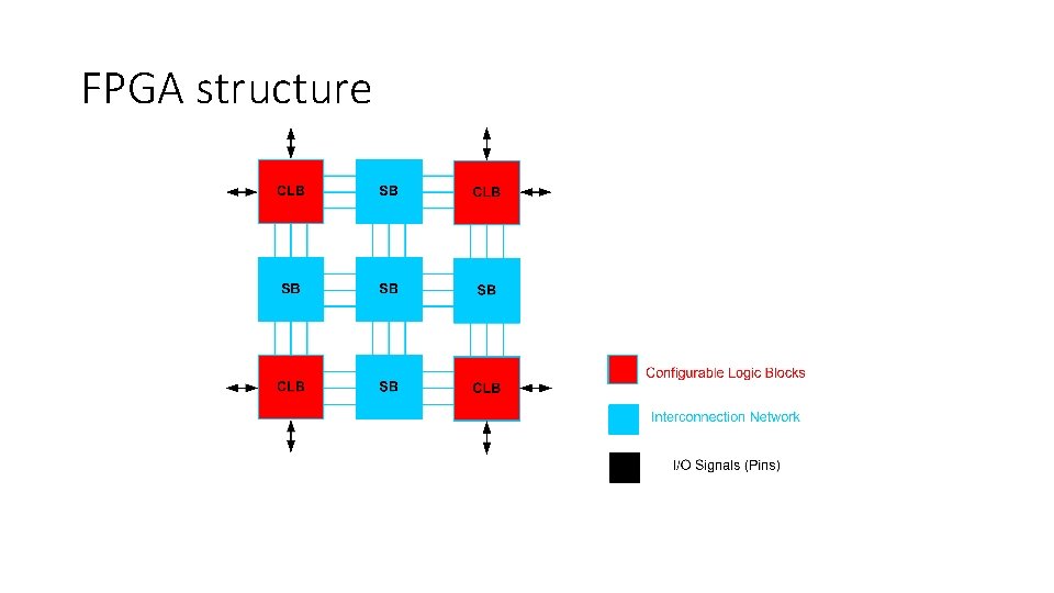
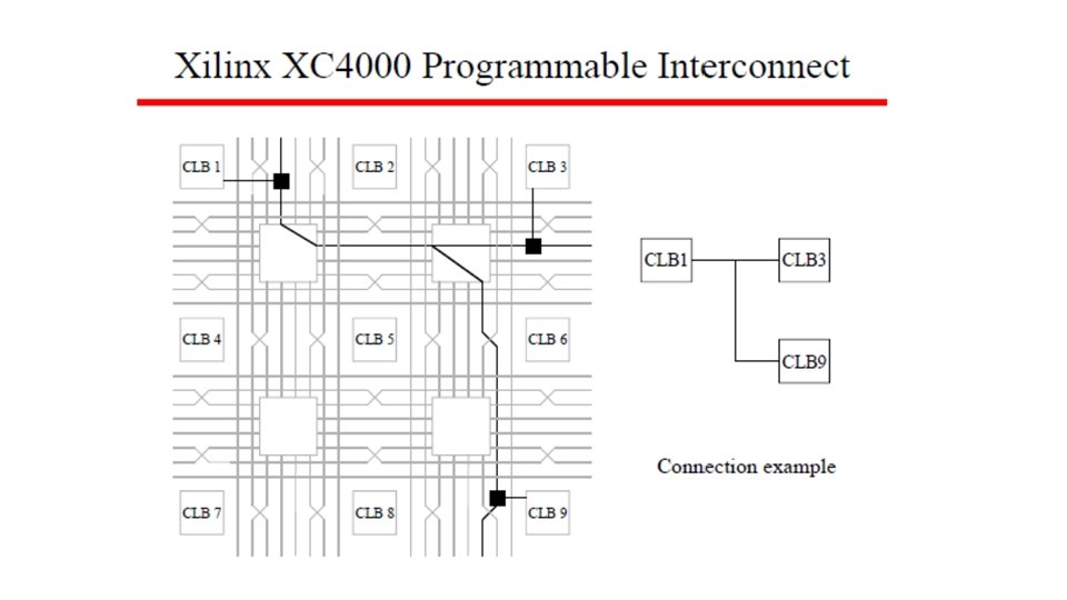
FPGA Principles • A Field-Programmable Gate Array (FPGA) is an integrated circuit that can be configured by the user to emulate any digital circuit as long as there are enough resources • An FPGA can be seen as an array of Configurable Logic Blocks (CLBs) connected through programmable interconnect (Switch Boxes)

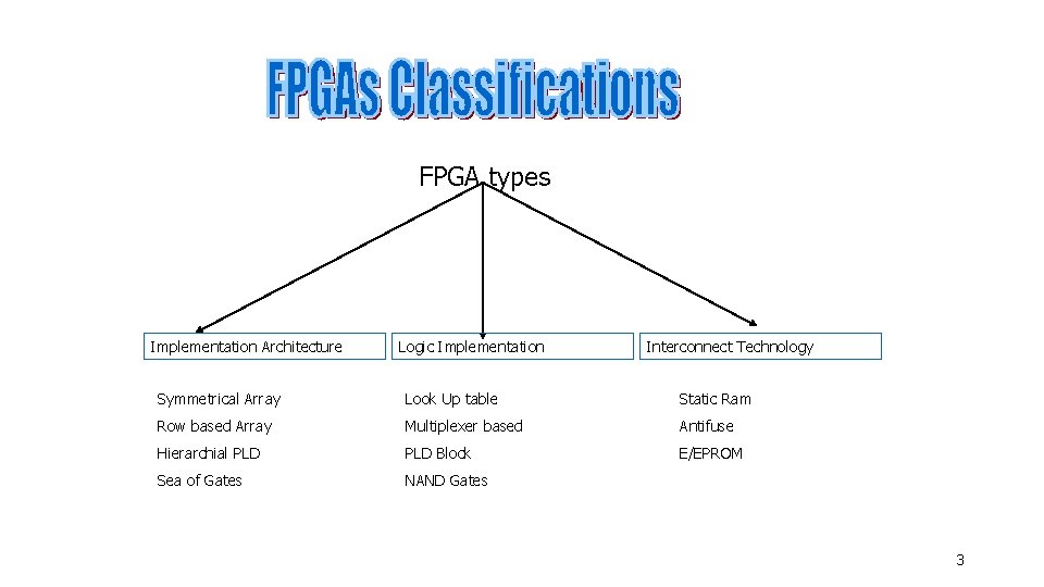
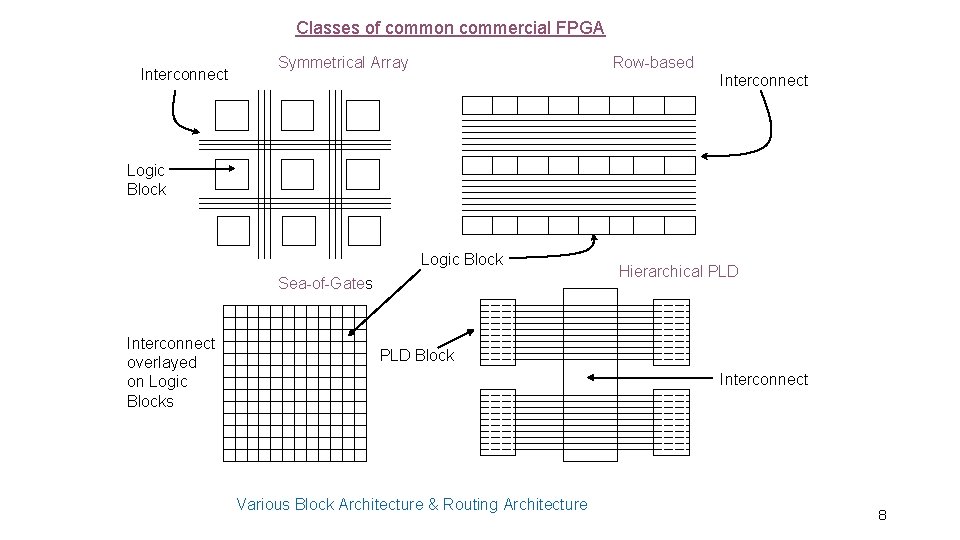
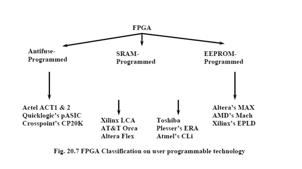
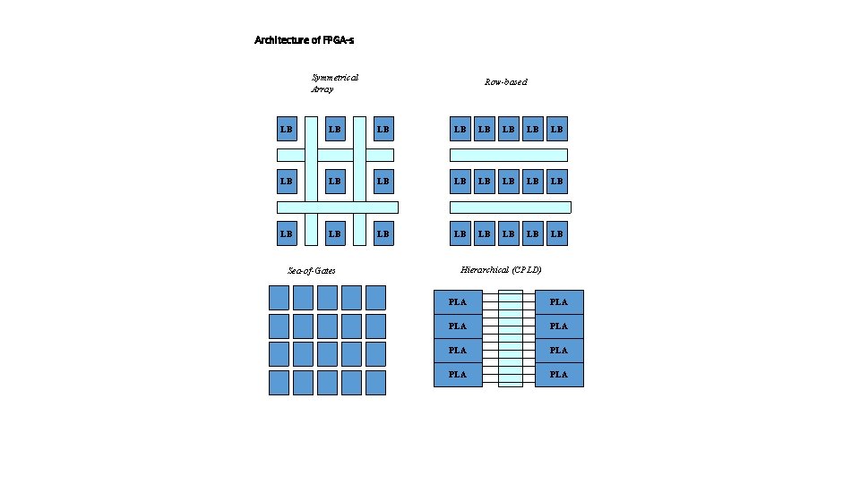
FPGA types Implementation Architecture Logic Implementation Interconnect Technology Symmetrical Array Look Up table Static Ram Row based Array Multiplexer based Antifuse Hierarchial PLD Block E/EPROM Sea of Gates NAND Gates 3

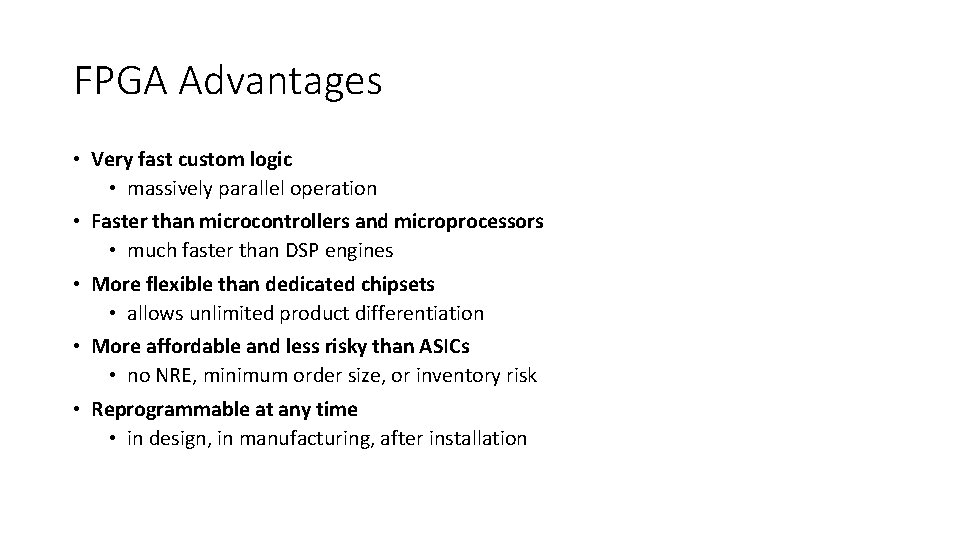
FPGA Advantages • Very fast custom logic • massively parallel operation • Faster than microcontrollers and microprocessors • much faster than DSP engines • More flexible than dedicated chipsets • allows unlimited product differentiation • More affordable and less risky than ASICs • no NRE, minimum order size, or inventory risk • Reprogrammable at any time • in design, in manufacturing, after installation

Manufacturers • Xilinx • Altera • Lattice • Actel We will work with XILINX FPGAs

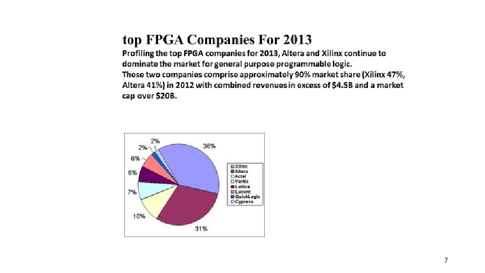
. June 2011 The 4 biggest FPGA producers are : Xilinx 2. 4 Billion$ in 2011 49% of US mrket Altera 40% 1. Billion 955 Quick Logic 1% 26 Million$ Micri. Semi 4% 207 Million $ Lattice Semi 6% 297 Million Xilinx and Altera have 89% of the Market With the top two FPGA companies taking up 89% of the FPGA market, you can be forgiven for thinking there was no one else out there. Xilinx and Altera have done a good job of defending the duopoly but a few companies are gradually winning market share by targeting specific applications

7

Classes of common commercial FPGA Interconnect Symmetrical Array Row-based Interconnect Logic Block Sea-of-Gates Interconnect overlayed on Logic Blocks Hierarchical PLD Block Interconnect Various Block Architecture & Routing Architecture 8
![FPGAs 1 Company General Architecture Logic Block Type Programming Technology Xilinx Symmetrical Array Lookup FPGAs…. [1] Company General Architecture Logic Block Type Programming Technology Xilinx Symmetrical Array Look-up](https://slidetodoc.com/presentation_image_h/cb496402b2c1d04aff7fa784f2296b11/image-9.jpg)
FPGAs…. [1] Company General Architecture Logic Block Type Programming Technology Xilinx Symmetrical Array Look-up Table Static RAM Actel Row-based Multiplexer-Based Anti-fuse Altera Hierarchical-PLD Block EPROM Plessey Sea-of-Gates NAND-gate Static RAM PLUS Hierarchical-PLD Block EPROM AMD Hierarchical-PLD Block EEPROM Quick. Logic Symmetrical Array Multiplexer-Based Anti-fuse Algotronix Sea-of-gates Multiplexers & Basic Gate Static RAM Concurrent Sea-of-gates Multiplexers & Basic Gate Static RAM Crosspoint Row-based Transistors Pairs & Multiplexers Anti-fuse Table 2. 2 Summary of Commercially Available FPGAs 9

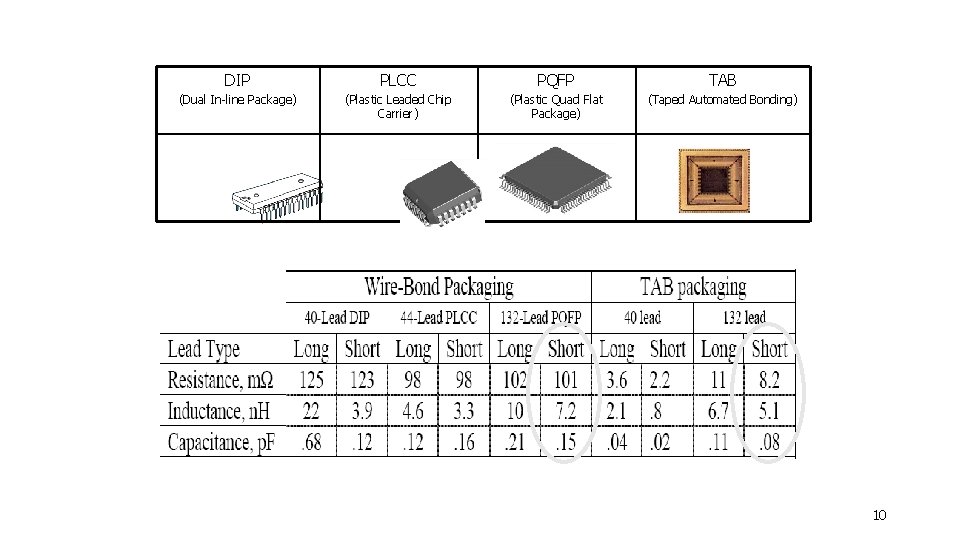
DIP PLCC PQFP TAB (Dual In-line Package) (Plastic Leaded Chip Carrier) (Plastic Quad Flat Package) (Taped Automated Bonding) 10


General structure of an FPGA The Design Warrior’s Guide to FPGAs Devices, Tools, and Flows. ISBN 0750676043 Copyright © 2004 Mentor Graphics Corp. (www. mentor. com)


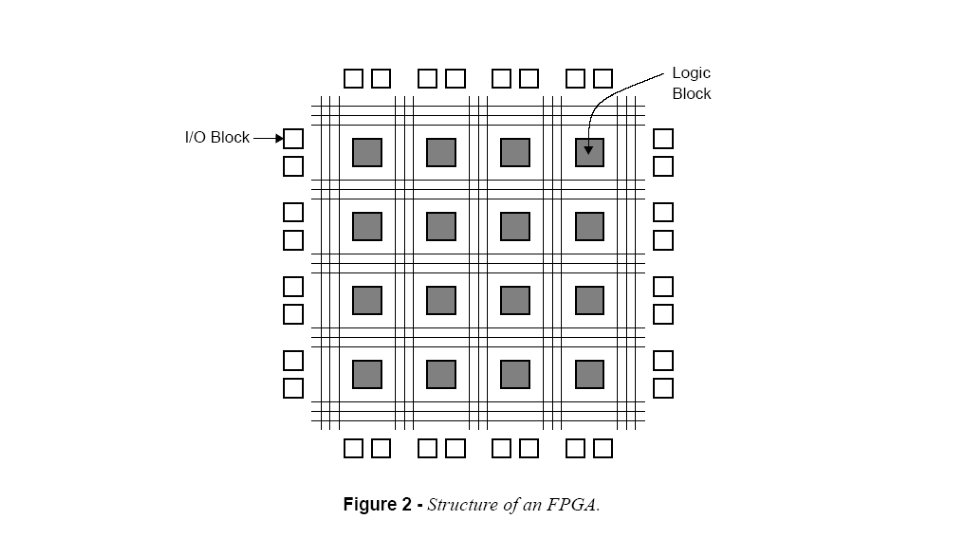
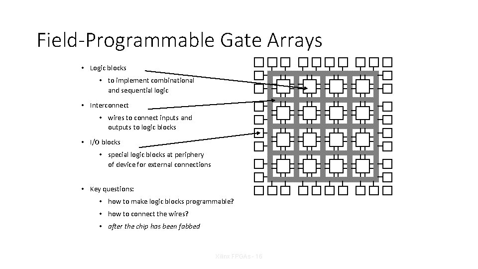
Field-Programmable Gate Arrays • Logic blocks • to implement combinational and sequential logic • Interconnect • wires to connect inputs and outputs to logic blocks • I/O blocks • special logic blocks at periphery of device for external connections • Key questions: • how to make logic blocks programmable? • how to connect the wires? • after the chip has been fabbed Xilinx FPGAs - 16

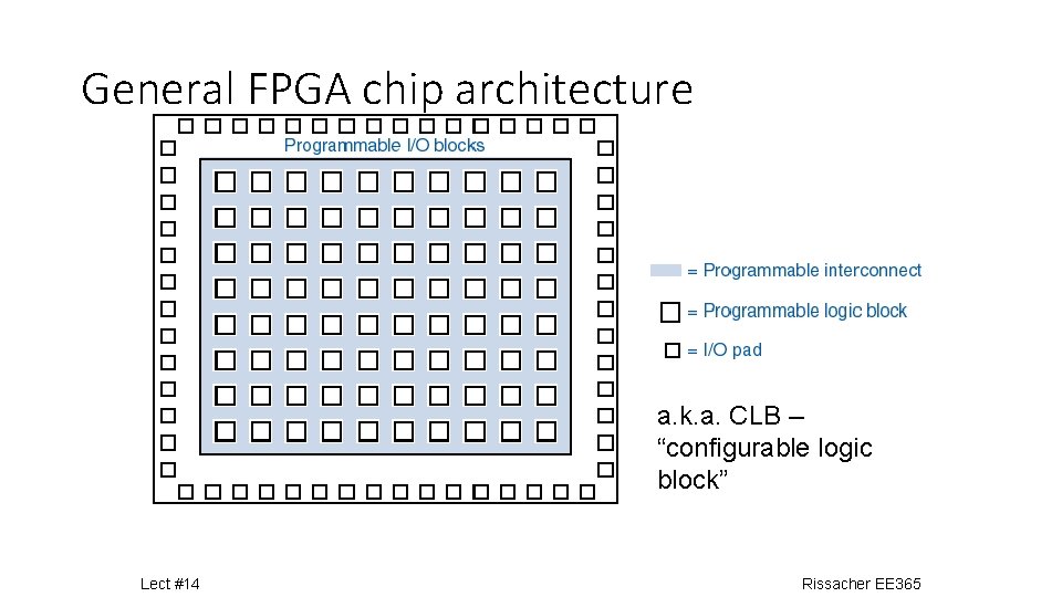
General FPGA chip architecture a. k. a. CLB -“configurable logic block” Lect #14 Rissacher EE 365

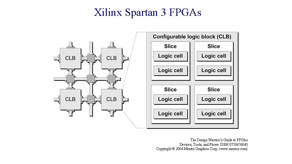
Xilinx Spartan 3 FPGAs The Design Warrior’s Guide to FPGAs Devices, Tools, and Flows. ISBN 0750676043 Copyright © 2004 Mentor Graphics Corp. (www. mentor. com)

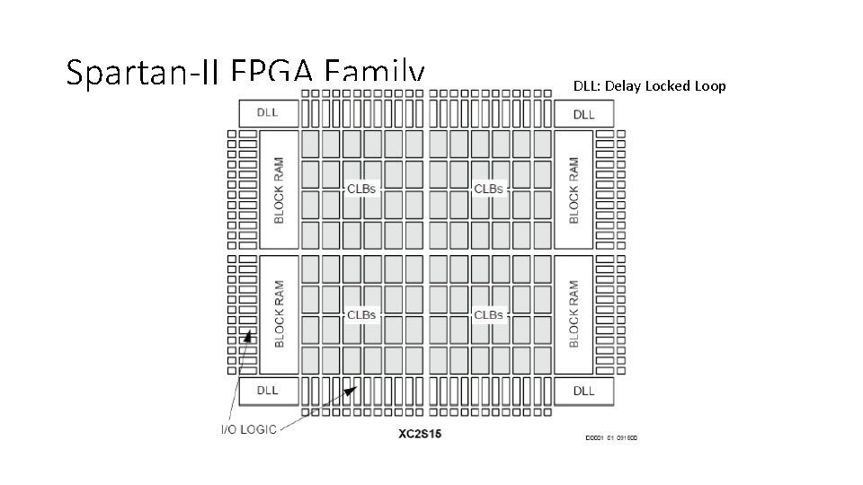
Spartan-II FPGA Family DLL: Delay Locked Loop

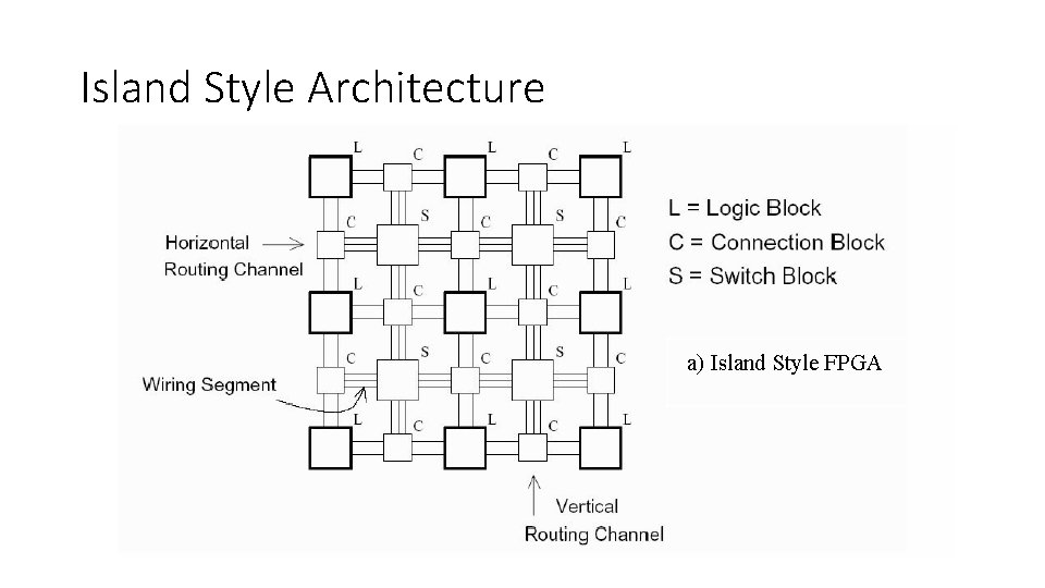
Island Style Architecture

CONCEPTUAL FPGA Interconnect Resources Logic Block I/O Cell 21

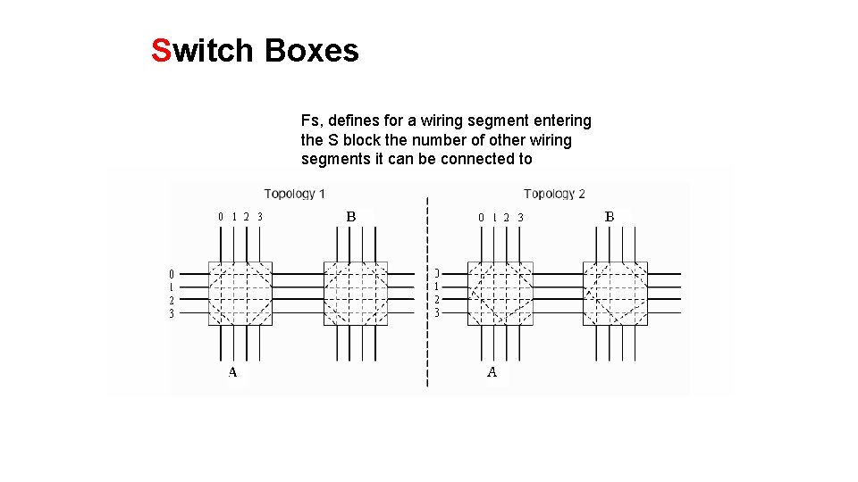
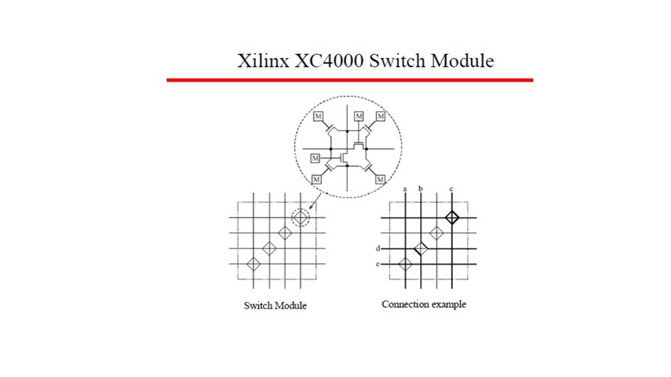
Switch Boxes Fs, defines for a wiring segment entering the S block the number of other wiring segments it can be connected to

Routings using C and S Boxes

Routing Algorithms • Maze Router • A* Search Routing • The Pathfinder


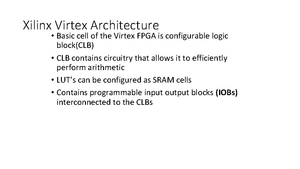
Xilinx Virtex Architecture • Basic cell of the Virtex FPGA is configurable logic block(CLB) • CLB contains circuitry that allows it to efficiently perform arithmetic • LUT’s can be configured as SRAM cells • Contains programmable input output blocks (IOBs) interconnected to the CLBs

FPGA - Field Programmable Gate Array S/V block I/O Cell LB Logic Block LB Logic Block S/V block I/O Cell LB Logic Block S/V block I/O Cell

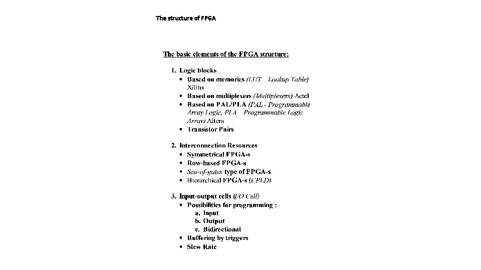
The structure of FPGA

Architecture of FPGA-s Symmetrical Array Row-based LB LB LB LB LB LB Sea-of-Gates Hierarchical (CPLD) PLA PLA

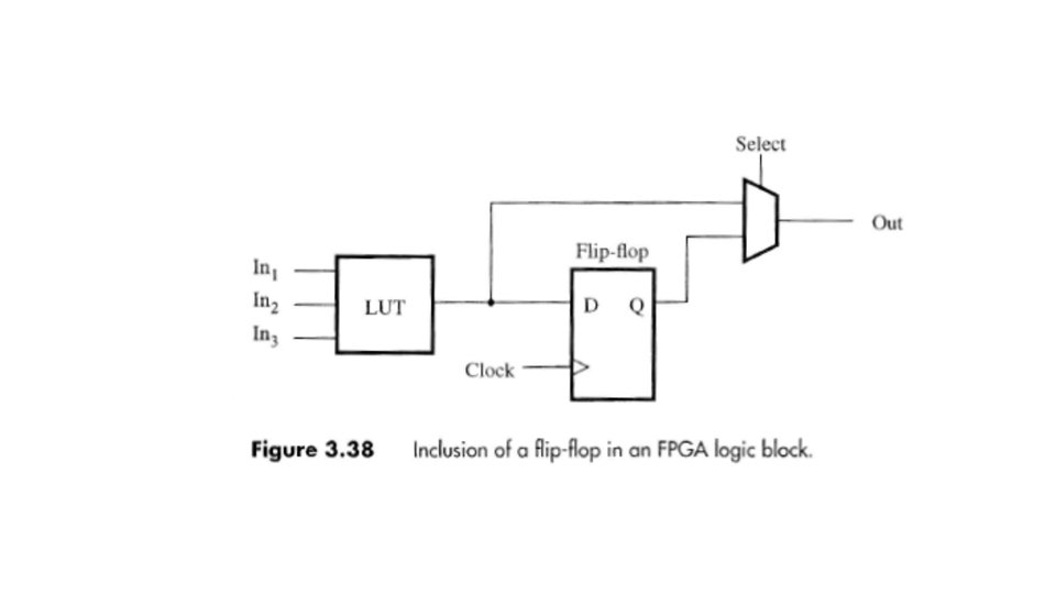
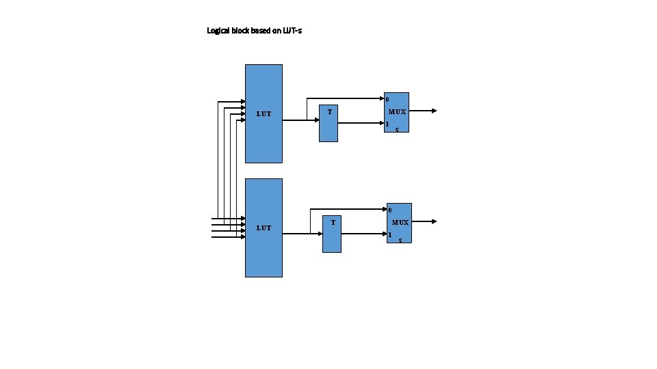
Logical block based on LUT-s 0 LUT T MUX 1 S

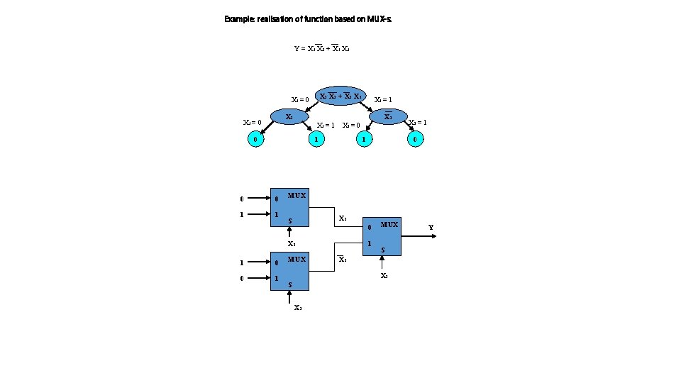
Example: realisation of function based on MUX-s. Y = X 1 X 2 + X 1 X 3 X 1 = 0 X 1 = 1 X 3 = 0 X 2 X 3 = 1 X 2 = 0 0 1 1 1 0 0 1 0 MUX X 3 S 0 X 3 1 X 2 = 1 MUX S X 2 X 1 S X 2 Y

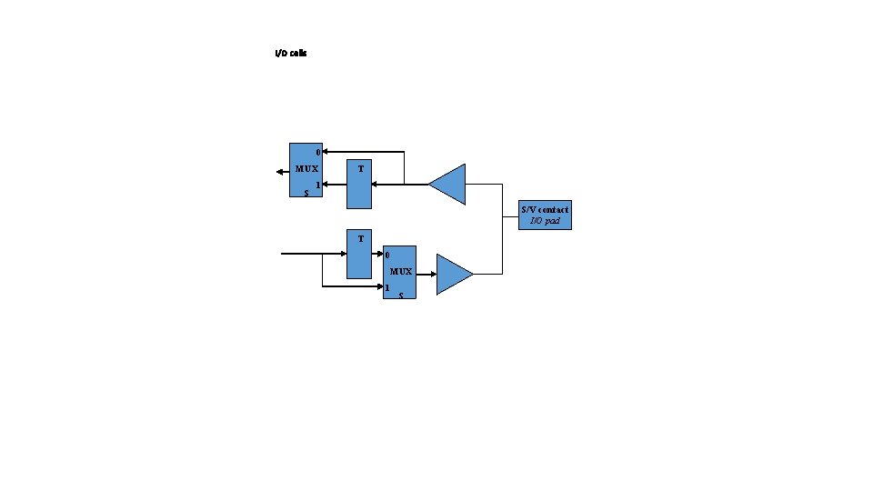
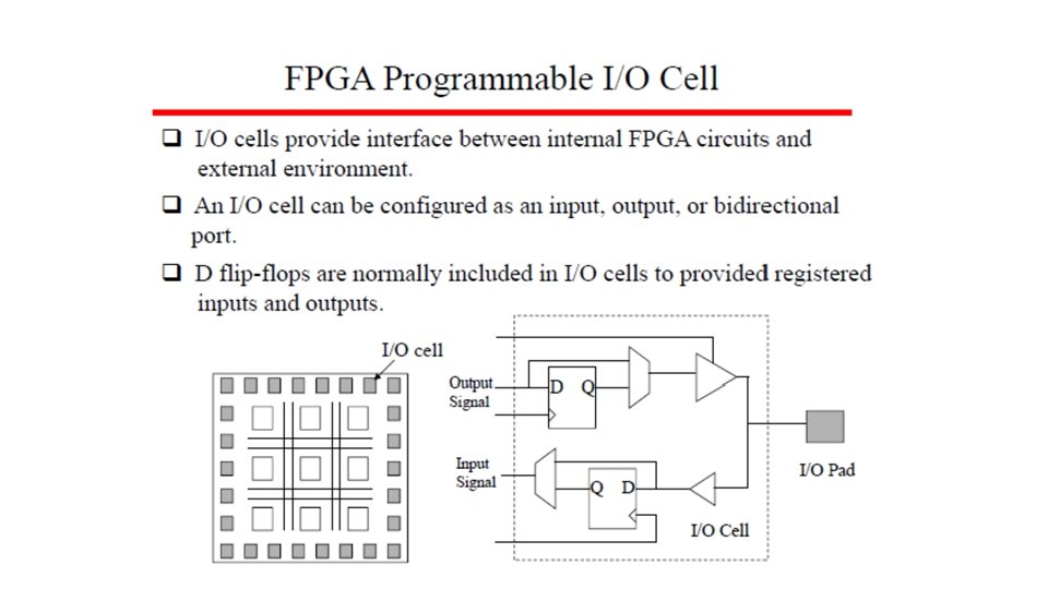
I/O cells 0 MUX S T 1 S/V contact I/O pad T 0 MUX 1 S


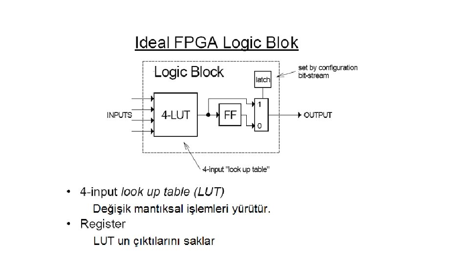
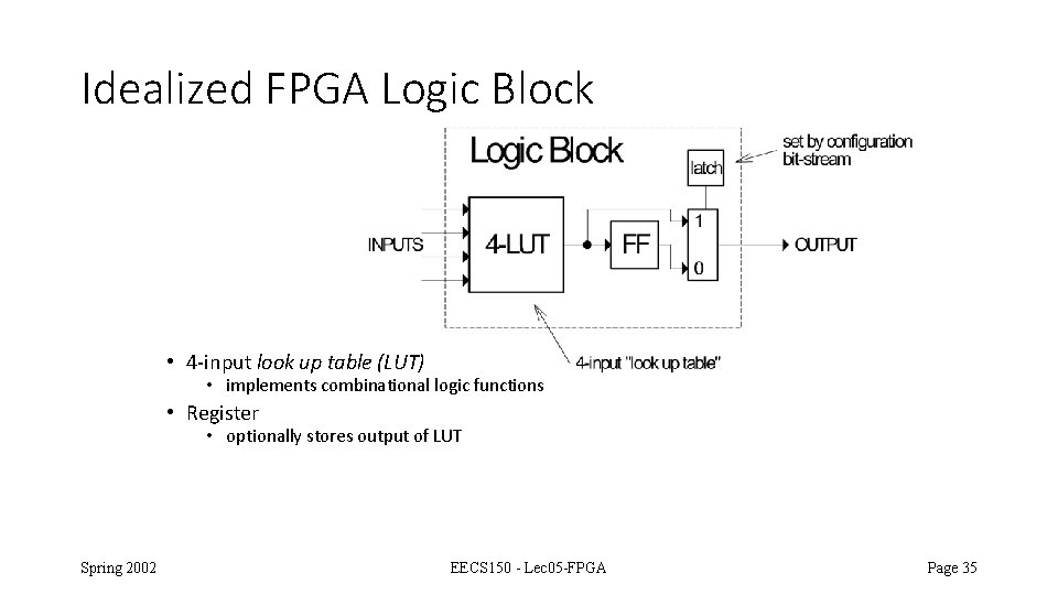
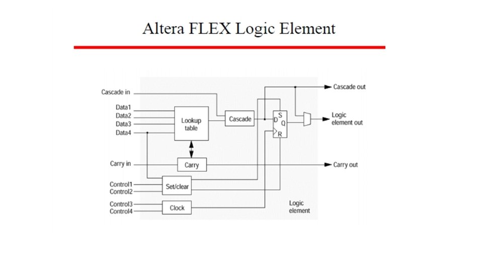
Idealized FPGA Logic Block • 4 -input look up table (LUT) • implements combinational logic functions • Register • optionally stores output of LUT Spring 2002 EECS 150 - Lec 05 -FPGA Page 35

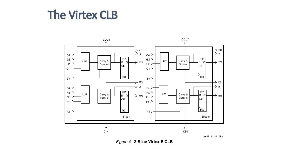
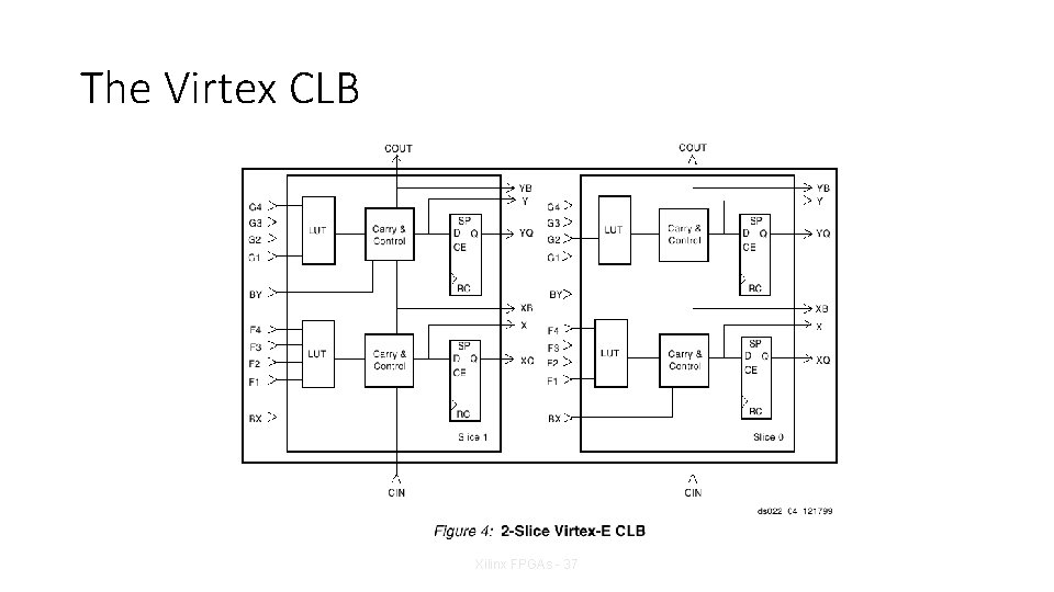
The Virtex CLB

The Virtex CLB Xilinx FPGAs - 37

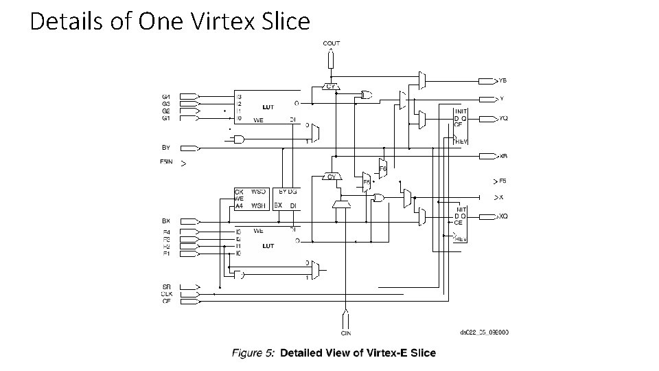
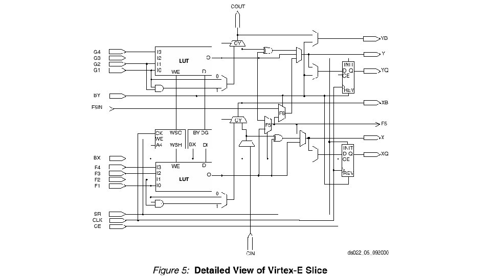
Details of One Virtex Slice Xilinx FPGAs - 38


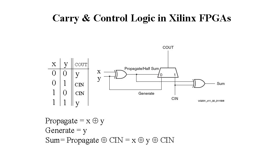
Carry & Control Logic in Xilinx FPGAs x 0 0 1 1 y COUT 0 y 1 CIN 0 CIN 1 y x y Propagate = x y Generate = y Sum= Propagate CIN = x y CIN

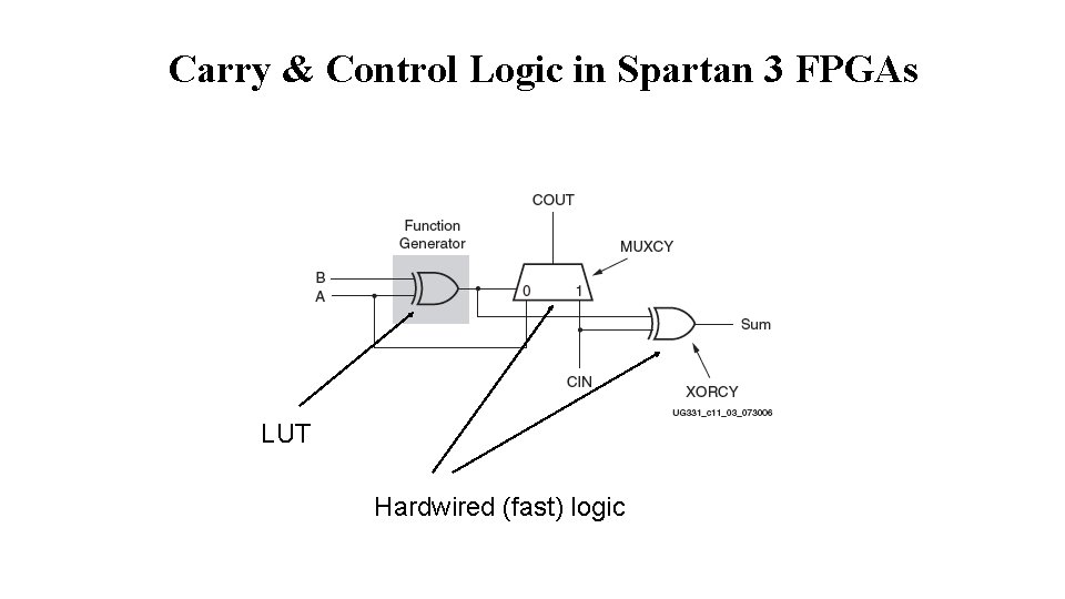
Carry & Control Logic in Spartan 3 FPGAs LUT Hardwired (fast) logic

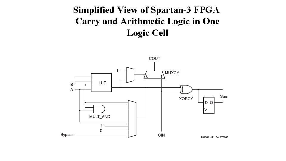
Simplified View of Spartan-3 FPGA Carry and Arithmetic Logic in One Logic Cell

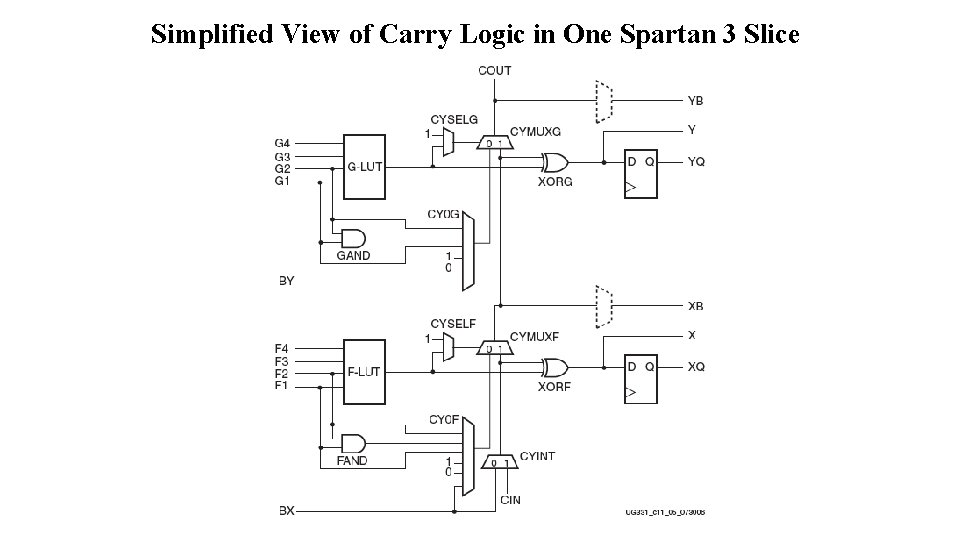
Simplified View of Carry Logic in One Spartan 3 Slice

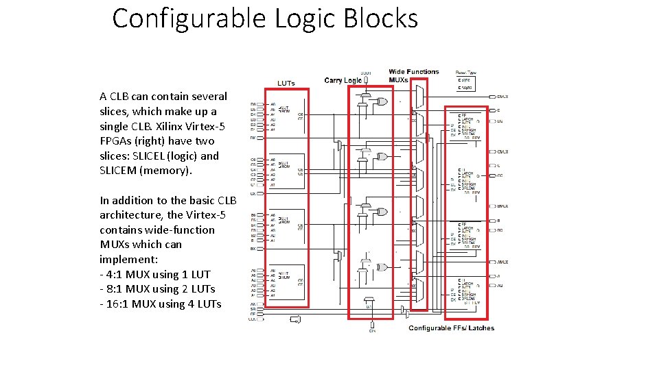
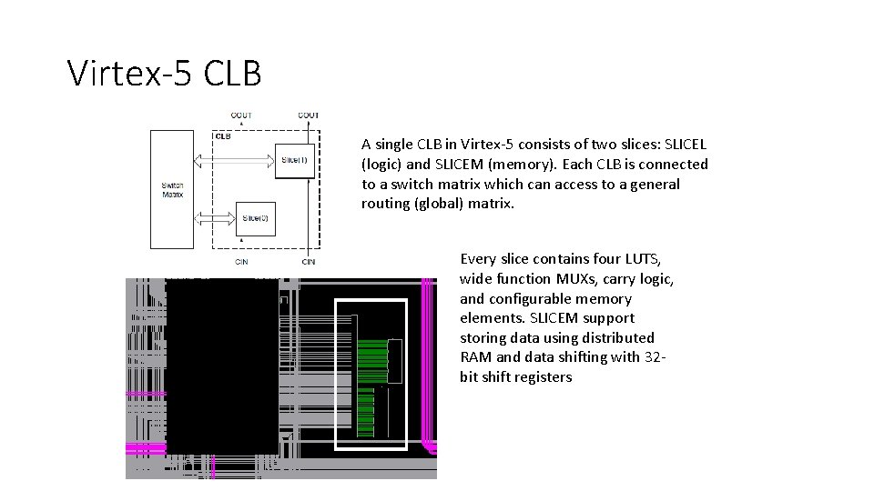
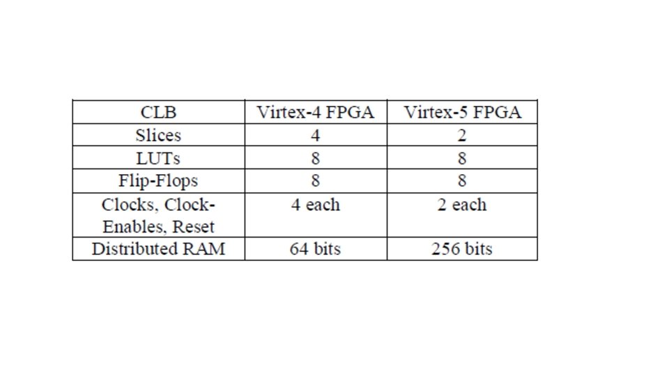
Configurable Logic Blocks A CLB can contain several slices, which make up a single CLB. Xilinx Virtex-5 FPGAs (right) have two slices: SLICEL (logic) and SLICEM (memory). In addition to the basic CLB architecture, the Virtex-5 contains wide-function MUXs which can implement: - 4: 1 MUX using 1 LUT - 8: 1 MUX using 2 LUTs - 16: 1 MUX using 4 LUTs

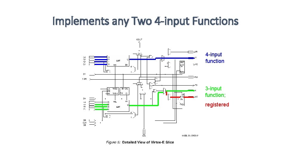
Implements any Two 4 -input Functions 4 -input function 3 -input function; registered

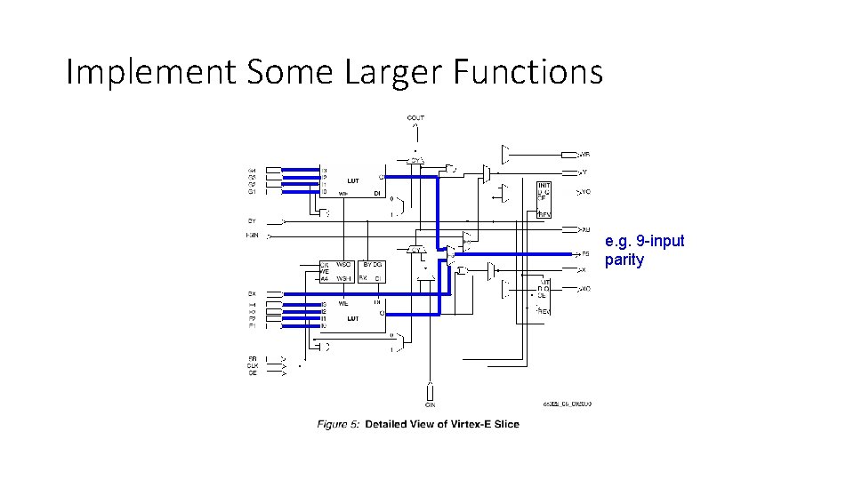
Implement Some Larger Functions e. g. 9 -input parity

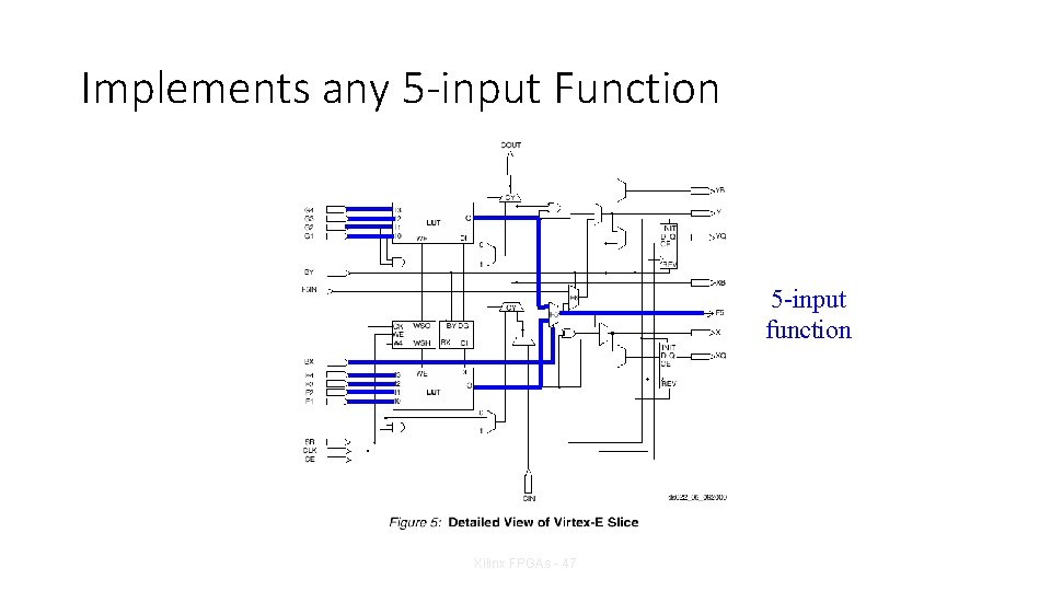
Implements any 5 -input Function 5 -input function Xilinx FPGAs - 47

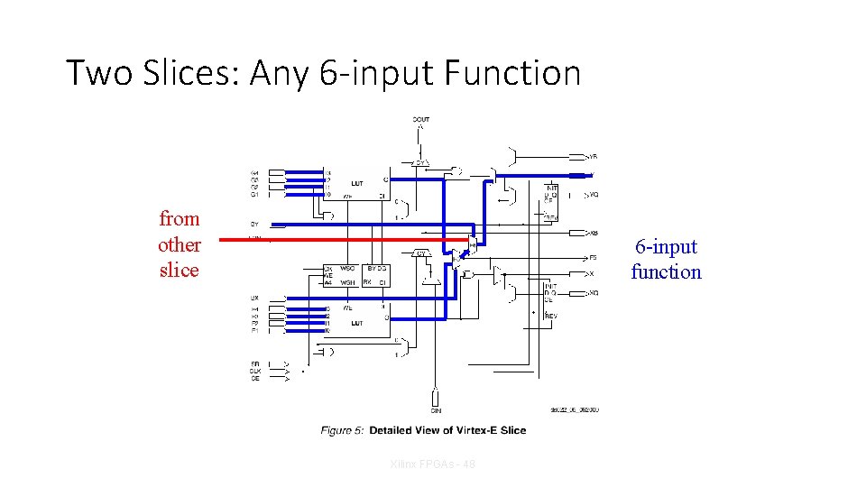
Two Slices: Any 6 -input Function from other slice 6 -input function Xilinx FPGAs - 48

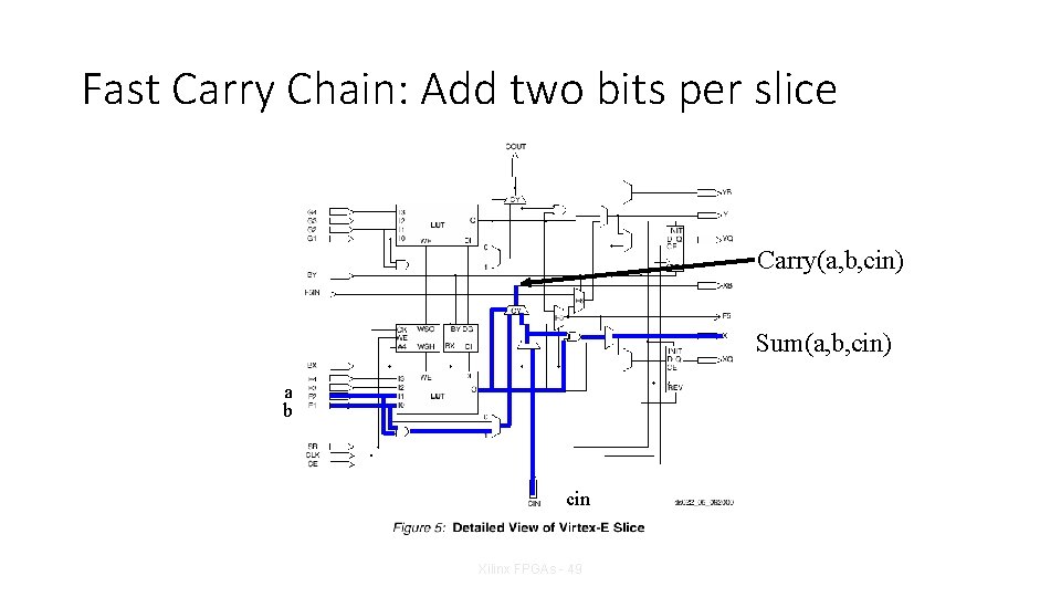
Fast Carry Chain: Add two bits per slice Carry(a, b, cin) Sum(a, b, cin) a b cin Xilinx FPGAs - 49
![Lookup Tables used as memory 16 x 2 Distributed Memory Xilinx FPGAs Lookup Tables used as memory (16 x 2) [ Distributed Memory ] Xilinx FPGAs](https://slidetodoc.com/presentation_image_h/cb496402b2c1d04aff7fa784f2296b11/image-50.jpg)
Lookup Tables used as memory (16 x 2) [ Distributed Memory ] Xilinx FPGAs - 50

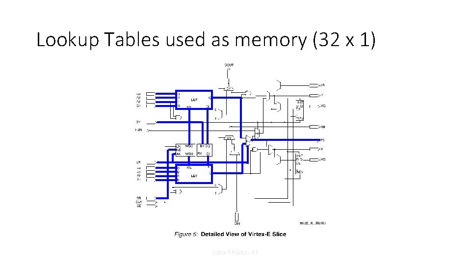
Lookup Tables used as memory (32 x 1) Xilinx FPGAs - 51

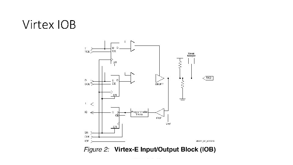
Virtex IOB Xilinx FPGAs - 52

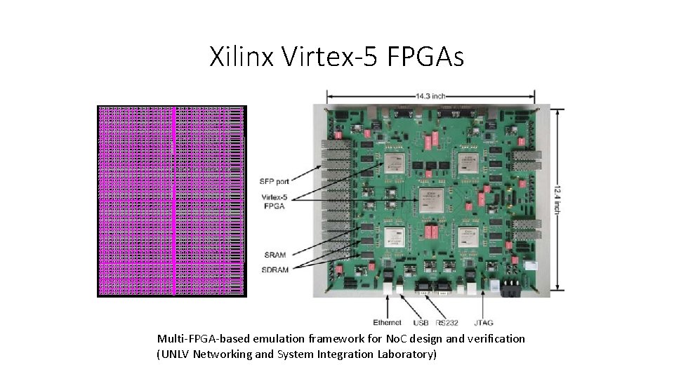
Xilinx Virtex-5 FPGAs Multi-FPGA-based emulation framework for No. C design and verification (UNLV Networking and System Integration Laboratory)

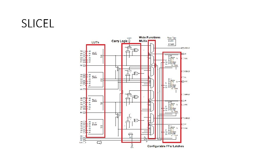
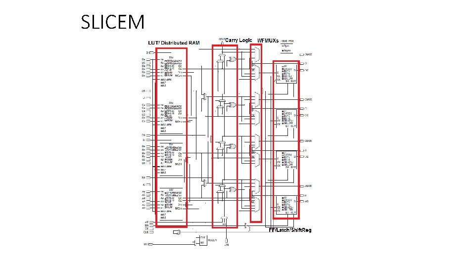
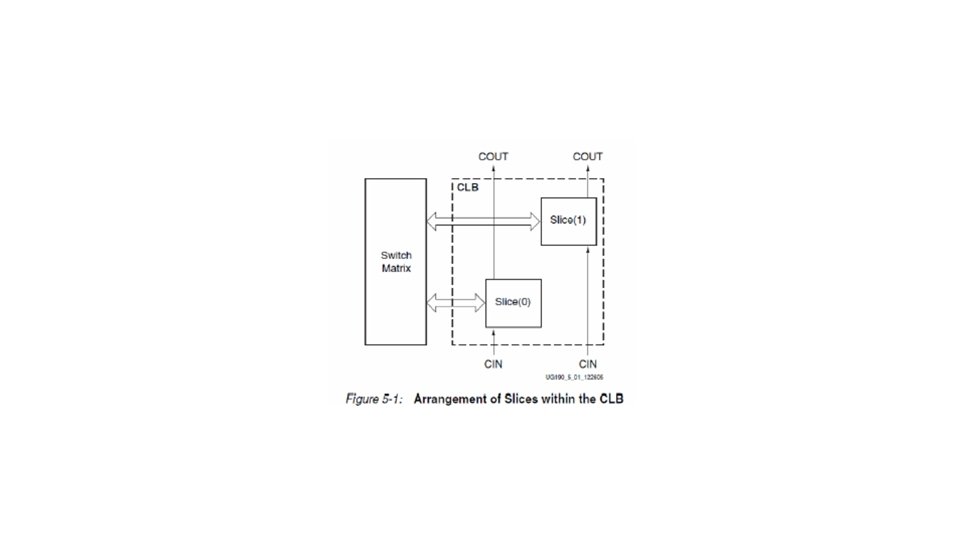
Virtex-5 CLB A single CLB in Virtex-5 consists of two slices: SLICEL (logic) and SLICEM (memory). Each CLB is connected to a switch matrix which can access to a general routing (global) matrix. Every slice contains four LUTS, wide function MUXs, carry logic, and configurable memory elements. SLICEM support storing data using distributed RAM and data shifting with 32 bit shift registers

SLICEL

SLICEM

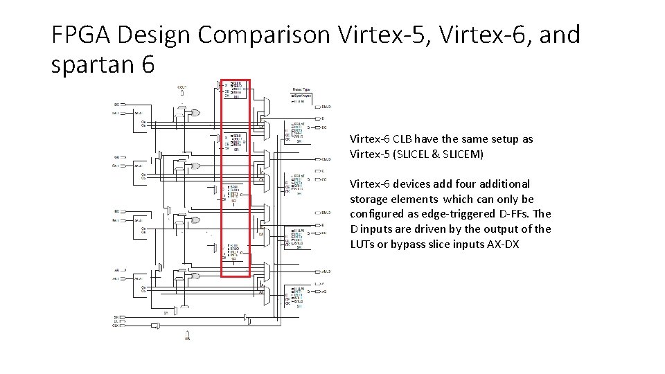
FPGA Design Comparison Virtex-5, Virtex-6, and spartan 6 Virtex-6 CLB have the same setup as Virtex-5 (SLICEL & SLICEM) Virtex-6 devices add four additional storage elements which can only be configured as edge-triggered D-FFs. The D inputs are driven by the output of the LUTs or bypass slice inputs AX-DX


FPGA structure

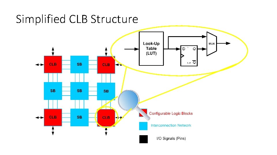
Simplified CLB Structure

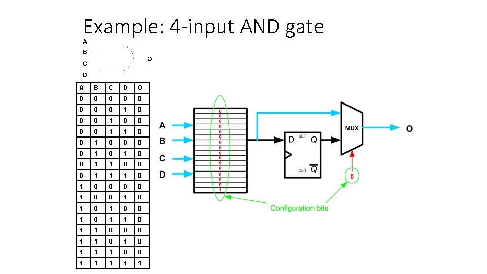
Example: 4 -input AND gate A B C D O 0 0 0 0 1 1 0 0 0 0 1 1 0 0 0 1 1 1 0 0 0 0 1 0 1 0 0 1 1 0 0 0 1 1 1 0 0 1 1 1

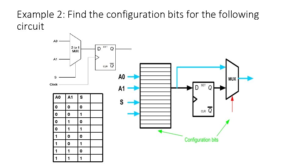
Example 2: Find the configuration bits for the following circuit A 0 A 1 S 0 0 0 1 1 1 0 0 1 1 1

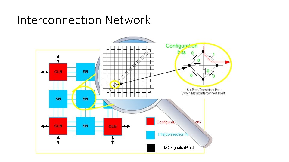
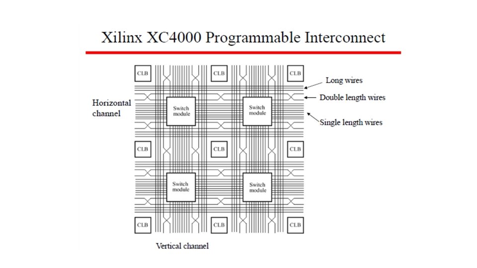
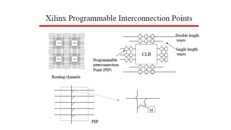
Interconnection Network

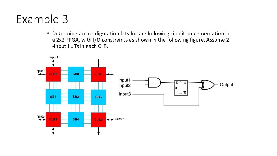
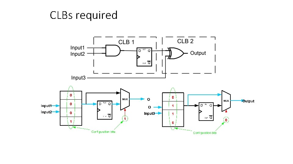
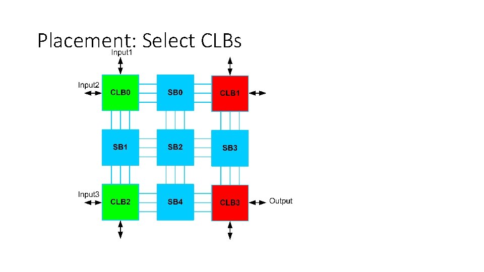
Example 3 • Determine the configuration bits for the following circuit implementation in a 2 x 2 FPGA, with I/O constraints as shown in the following figure. Assume 2 -input LUTs in each CLB.

CLBs required

Placement: Select CLBs

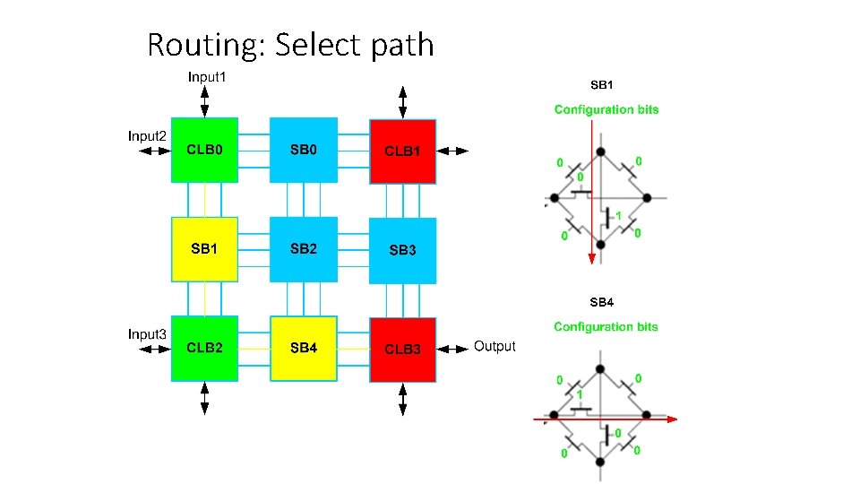
Routing: Select path

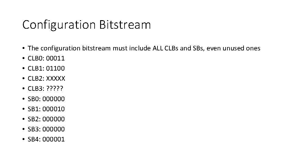
Configuration Bitstream • • • The configuration bitstream must include ALL CLBs and SBs, even unused ones CLB 0: 00011 CLB 1: 01100 CLB 2: XXXXX CLB 3: ? ? ? SB 0: 000000 SB 1: 000010 SB 2: 000000 SB 3: 000000 SB 4: 000001

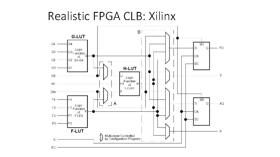
Realistic FPGA CLB: Xilinx

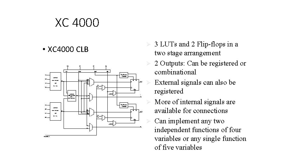
XC 4000 • XC 4000 CLB Ø Ø Ø 3 LUTs and 2 Flip-flops in a two stage arrangement 2 Outputs: Can be registered or combinational External signals can also be registered More of internal signals are available for connections Can implement any two independent functions of four variables or any single function of five variables

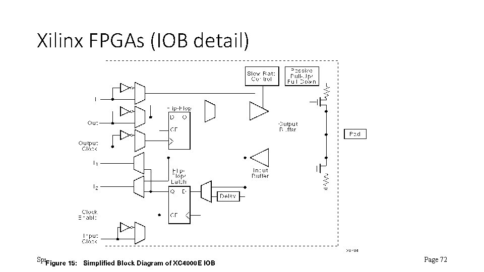
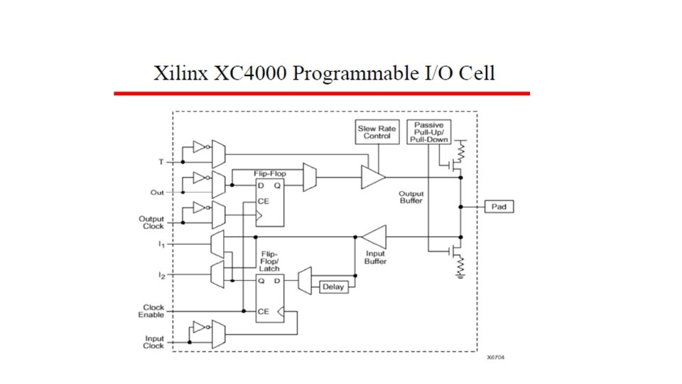
Xilinx FPGAs (IOB detail) Spring 2002 EECS 150 - Lec 05 -FPGA Page 72

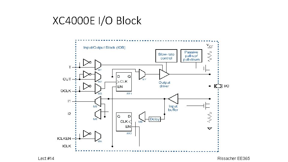
XC 4000 E I/O Block Lect #14 Rissacher EE 365


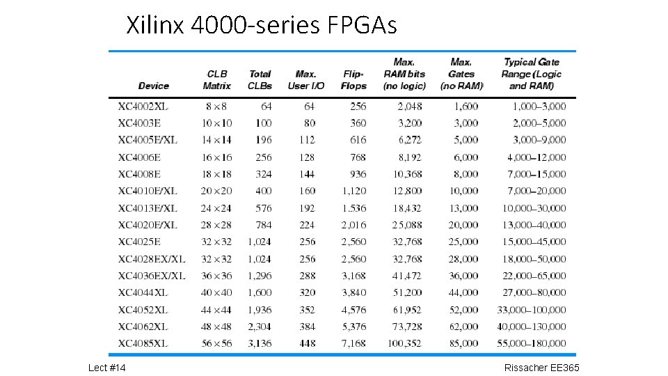
Xilinx 4000 -series FPGAs Lect #14 Rissacher EE 365

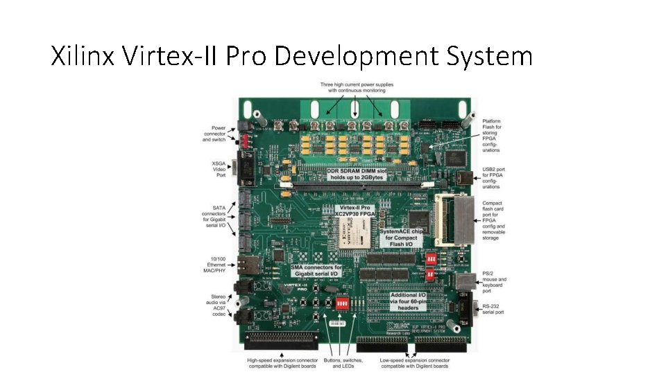
Xilinx Virtex-II Pro Development System

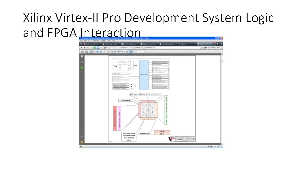
Xilinx Virtex-II Pro Development System Logic and FPGA Interaction

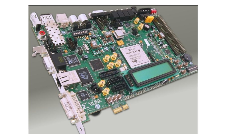
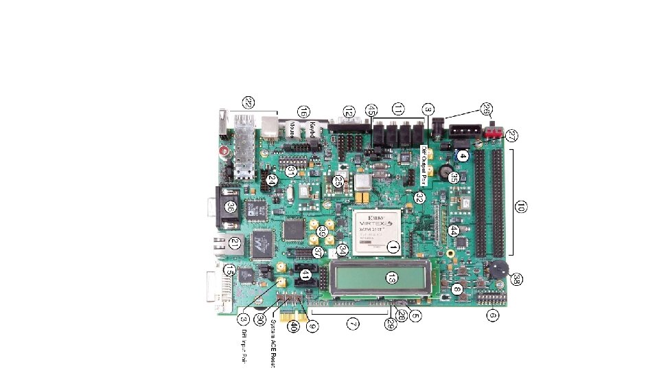
Xilinx Virtex 5 Development System (Front)

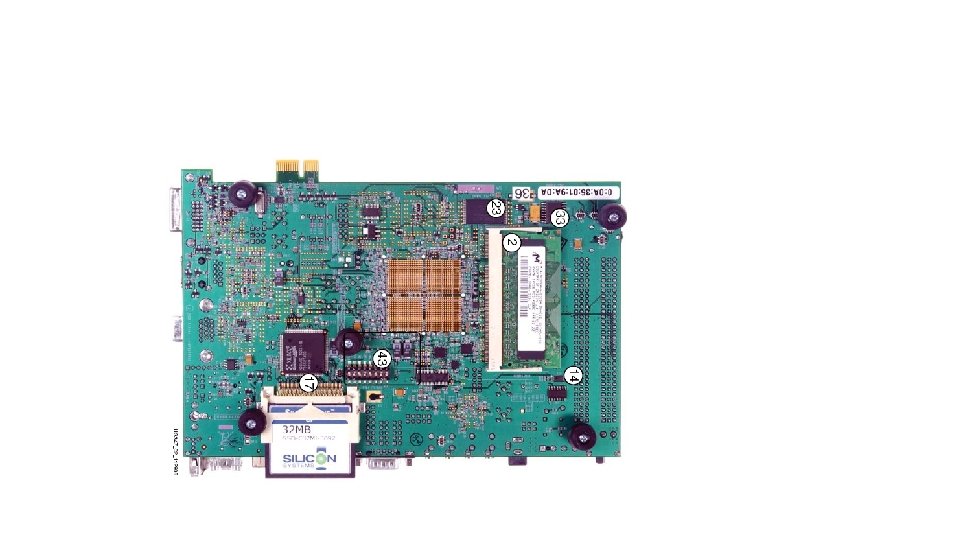
Xilinx Virtex 5 Development System (Back)

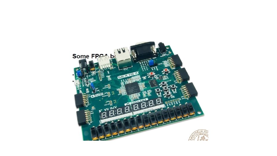
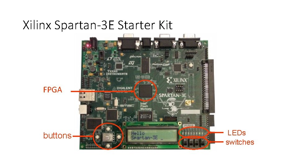
Xilinx Spartan-3 E Starter Kit FPGA buttons LEDs switches

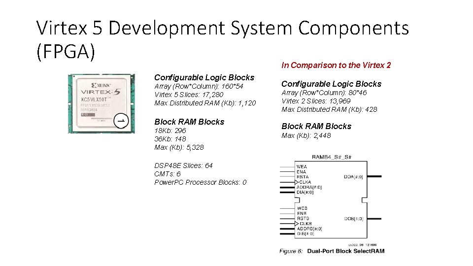
Virtex 5 Development System Components (FPGA) In Comparison to the Virtex 2 Configurable Logic Blocks Array (Row*Column): 160*54 Virtex 5 Slices: 17, 280 Max Distributed RAM (Kb): 1, 120 Block RAM Blocks 18 Kb: 296 36 Kb: 148 Max (Kb): 5, 328 DSP 48 E Slices: 64 CMTs: 6 Power. PC Processor Blocks: 0 Configurable Logic Blocks Array (Row*Column): 80*46 Virtex 2 Slices: 13, 969 Max Distributed RAM (Kb): 428 Block RAM Blocks Max (Kb): 2, 448

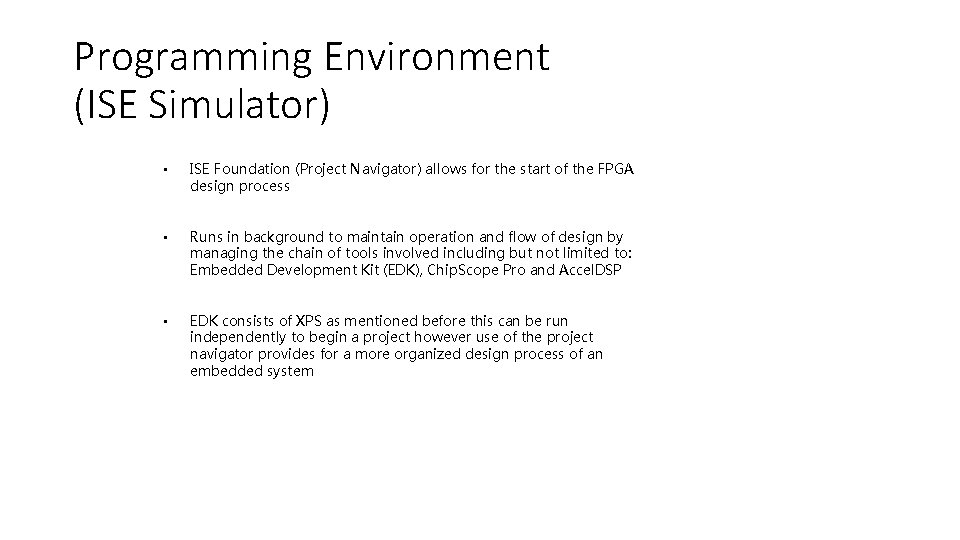
Programming Environment (ISE Simulator) • ISE Foundation (Project Navigator) allows for the start of the FPGA design process • Runs in background to maintain operation and flow of design by managing the chain of tools involved including but not limited to: Embedded Development Kit (EDK), Chip. Scope Pro and Accel. DSP • EDK consists of XPS as mentioned before this can be run independently to begin a project however use of the project navigator provides for a more organized design process of an embedded system

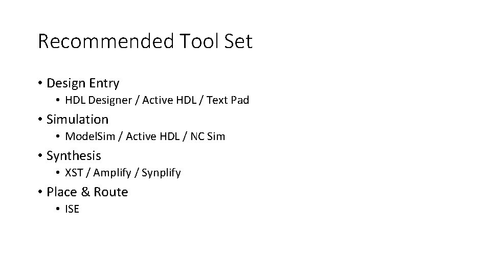
Recommended Tool Set • Design Entry • HDL Designer / Active HDL / Text Pad • Simulation • Model. Sim / Active HDL / NC Sim • Synthesis • XST / Amplify / Synplify • Place & Route • ISE

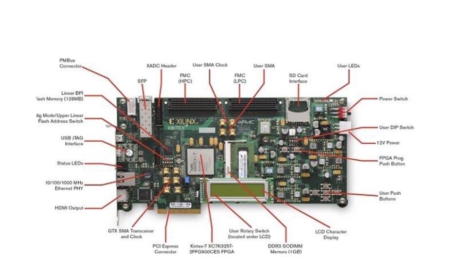
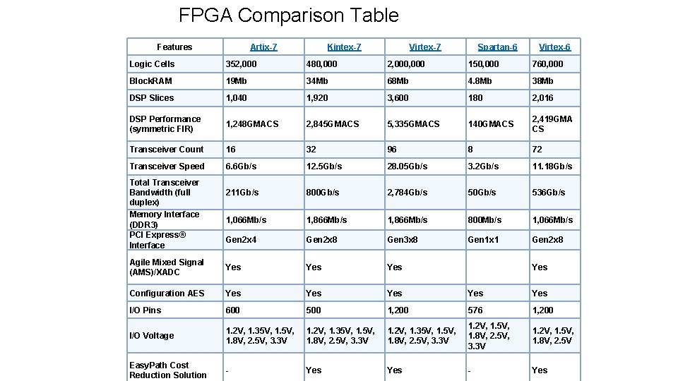
FPGA Comparison Table Features Artix-7 Kintex-7 Virtex-7 Spartan-6 Virtex-6 Logic Cells 352, 000 480, 000 2, 000 150, 000 760, 000 Block. RAM 19 Mb 34 Mb 68 Mb 4. 8 Mb 38 Mb DSP Slices 1, 040 1, 920 3, 600 180 2, 016 DSP Performance (symmetric FIR) 1, 248 GMACS 2, 845 GMACS 5, 335 GMACS 140 GMACS 2, 419 GMA CS Transceiver Count 16 32 96 8 72 Transceiver Speed 6. 6 Gb/s 12. 5 Gb/s 28. 05 Gb/s 3. 2 Gb/s 11. 18 Gb/s 211 Gb/s 800 Gb/s 2, 784 Gb/s 50 Gb/s 536 Gb/s 1, 066 Mb/s 1, 866 Mb/s 800 Mb/s 1, 066 Mb/s Gen 2 x 4 Gen 2 x 8 Gen 3 x 8 Gen 1 x 1 Gen 2 x 8 Agile Mixed Signal (AMS)/XADC Yes Yes Configuration AES Yes Yes Yes I/O Pins 600 500 1, 200 576 1, 200 I/O Voltage 1. 2 V, 1. 35 V, 1. 5 V, 1. 8 V, 2. 5 V, 3. 3 V 1. 2 V, 1. 5 V, 1. 8 V, 2. 5 V, 3. 3 V 1. 2 V, 1. 5 V, 1. 8 V, 2. 5 V Easy. Path Cost Reduction Solution - Yes Total Transceiver Bandwidth (full duplex) Memory Interface (DDR 3) PCI Express® Interface

