Ramon Chips is named in memory of Col
 Me. V*cm Comparing FF alternatives Area Power Tvalid Unprotected LET CLK->out Threshold Errors/bit/day [@LEO](*) Me. V*cm](https://slidetodoc.com/presentation_image/5ee83ed6416b566aaa061d9ae9a959cc/image-11.jpg)
- Slides: 22

Ramon Chips is named in memory of Col. Ilan Ramon, Israeli astronaut who died on board the Columbia space shuttle, 1/2/2003 Development process of RHBD cell libraries for advanced SOCs Tuvia Liran [tuvia@ramon-chips. com ] Ran Ginosar [ran@ramon-chips. com ] Dov Alon [dov@ramon-chips. com ] Ramon-Chips Ltd. , Israel Ramon Chips

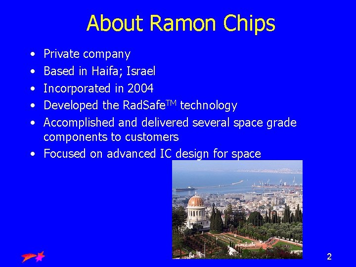
About Ramon Chips • • • Private company Based in Haifa; Israel Incorporated in 2004 Developed the Rad. Safe. TM technology Accomplished and delivered several space grade components to customers • Focused on advanced IC design for space Ramon Chips 2

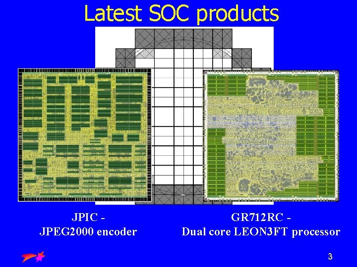
Latest SOC products JPIC JPEG 2000 encoder Ramon Chips GR 712 RC Dual core LEON 3 FT processor 3

Outline • • • Concepts of Rad. Safe. TM technology Rad. Safe. TM libraries Design considerations Development vehicles used Rad. Safe. TM 0. 13µ technology Ramon Chips 4

Rad. Safe. TM concepts • • Radiation Hardening is achieved only by design Same technology for all space applications Based on standard CMOS technology Radiation hardening guaranteed by similarity to previously qualified products/test chips • All IPs fully developed and owned by Ramon Chips • Proven immunity on Tower Semi 0. 18µ technology • Complementary methodologies: § § § Design For Reliability Flow for SEU/SET mitigation Design for testability Electrical screening Class S screening flow Ramon Chips 5

Radiation & Reliability effects mitigated by Rad. Safe. TM • Radiation effects: § § § TID SEL SEU/SET in flip-flops SEU in SRAMs SEFI caused by PLL/DLLs • Reliability effects: § § Electro-migration Thermal cycling Chemical effects Mechanical (shock & vibration) Ramon Chips 6

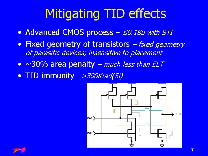
Mitigating TID effects • Advanced CMOS process – ≤ 0. 18µ with STI • Fixed geometry of transistors – fixed geometry of parasitic devices; insensitive to placement • ~30% area penalty – much less than ELT • TID immunity - >300 Krad(Si) Ramon Chips 7

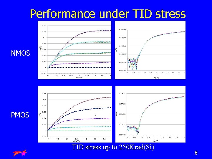
Performance under TID stress NMOS PMOS TID stress up to 250 Krad(Si) Ramon Chips 8

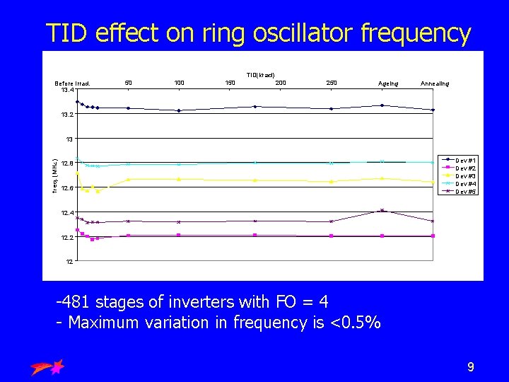
TID effect on ring oscillator frequency TID(krad) 0 Before Irrad. 13. 4 50 100 150 200 250 300 Ageing 350 Annealing 13. 2 freq. (MHz) 13 Dev #1 Dev #2 Dev #3 Dev #4 Dev #5 12. 8 12. 6 12. 4 12. 2 12 -481 stages of inverters with FO = 4 - Maximum variation in frequency is <0. 5% Ramon Chips 9

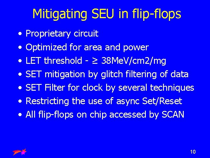
Mitigating SEU in flip-flops • • Proprietary circuit Optimized for area and power LET threshold - ≥ 38 Me. V/cm 2/mg SET mitigation by glitch filtering of data SET Filter for clock by several techniques Restricting the use of async Set/Reset All flip-flops on chip accessed by SCAN Ramon Chips 10
 Me. V*cm](https://slidetodoc.com/presentation_image/5ee83ed6416b566aaa061d9ae9a959cc/image-11.jpg)
Comparing FF alternatives Area Power Tvalid Unprotected LET CLK->out Threshold Errors/bit/day [@LEO](*) Me. V*cm 2/mg 1 1 1 2. 94 5 E-7 TMR 4. 01 2. 6 2. 5 - - DMR 2. 48 2. 2 2. 5 - - DMR+ 2. 34 2. 1 2. 5 38. 2 4 E-14 SEP 1. 8 1. 6 1. 2 38. 2 4 E-12 SER (**) 1. 75 1. 2 - - • Relative values • Refers to standard FF, with scan, same output drive (*) Refers to 37 o inclination, quite solar (**) Designed for 0. 13 u only Ramon Chips 11

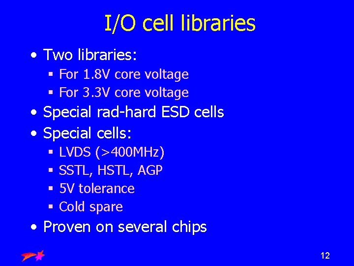
I/O cell libraries • Two libraries: § For 1. 8 V core voltage § For 3. 3 V core voltage • Special rad-hard ESD cells • Special cells: § § LVDS (>400 MHz) SSTL, HSTL, AGP 5 V tolerance Cold spare • Proven on several chips Ramon Chips 12

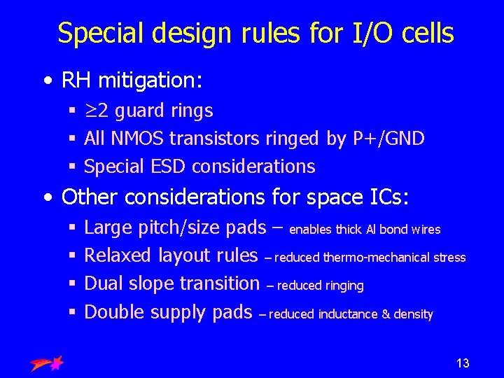
Special design rules for I/O cells • RH mitigation: § ≥ 2 guard rings § All NMOS transistors ringed by P+/GND § Special ESD considerations • Other considerations for space ICs: § § Large pitch/size pads – enables thick Al bond wires Relaxed layout rules – reduced thermo-mechanical stress Dual slope transition – reduced ringing Double supply pads – reduced inductance & density Ramon Chips 13

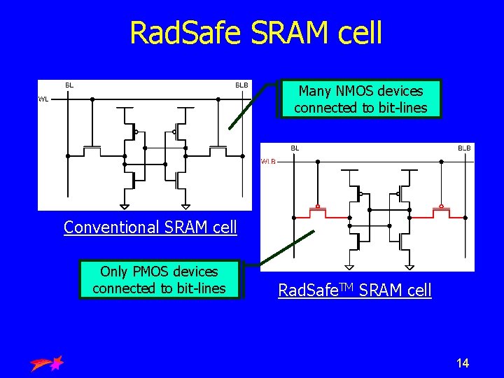
Rad. Safe SRAM cell Many NMOS devices connected to bit-lines Conventional SRAM cell Only PMOS devices connected to bit-lines Ramon Chips Rad. Safe. TM SRAM cell 14

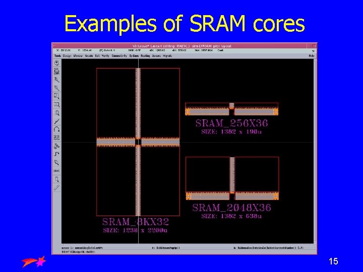
Examples of SRAM cores Ramon Chips 15

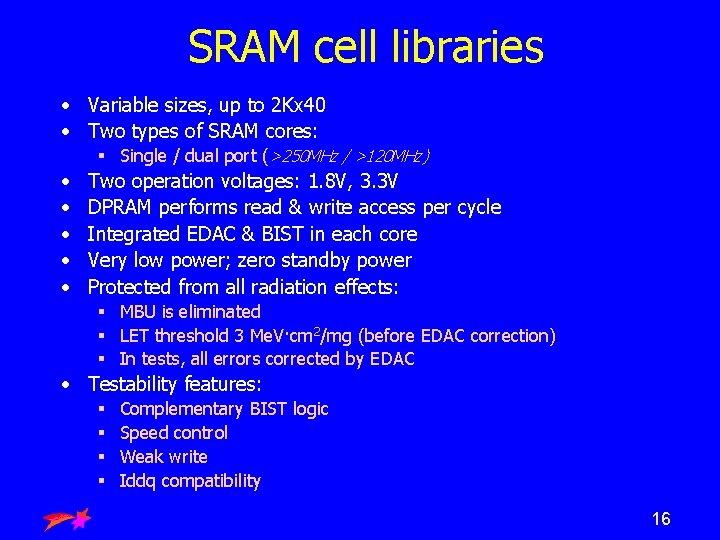
SRAM cell libraries • Variable sizes, up to 2 Kx 40 • Two types of SRAM cores: § Single / dual port (>250 MHz / >120 MHz) • • • Two operation voltages: 1. 8 V, 3. 3 V DPRAM performs read & write access per cycle Integrated EDAC & BIST in each core Very low power; zero standby power Protected from all radiation effects: § MBU is eliminated § LET threshold 3 Me. V·cm 2/mg (before EDAC correction) § In tests, all errors corrected by EDAC • Testability features: § § Complementary BIST logic Speed control Weak write Iddq compatibility Ramon Chips 16

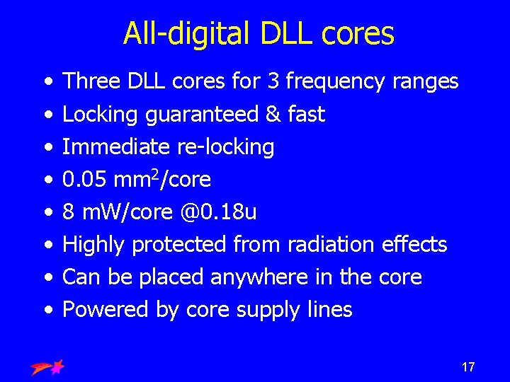
All-digital DLL cores • • Three DLL cores for 3 frequency ranges Locking guaranteed & fast Immediate re-locking 0. 05 mm 2/core 8 m. W/core @0. 18 u Highly protected from radiation effects Can be placed anywhere in the core Powered by core supply lines Ramon Chips 17

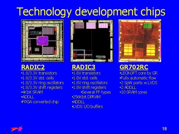
Technology development chips RADIC 2 • 1. 8/3. 3 V transistors • 1. 8/3. 3 V std. cells • 1. 8/3. 3 V ring oscillators • 1. 8/3. 3 V shift registers • 4 Kbit SRAM • ADDLL • FPGA converted chip RADIC 3 • 1. 8 V transistors • 1. 8 V std. cells • 1. 8 V ring oscillators • 1. 8 V shift registers • Several FF types • 256 Kbit DPRAM • ADDLL • LVDS I/O buffers Ramon Chips GR 702 RC • LEON 3 FT core by GR • Fully automatic flow • 2 Sp. W ports w LVDS • 2 ADDLL • 10 SRAM cores 18

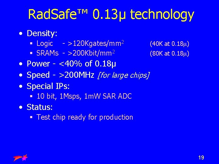
Rad. Safe™ 0. 13µ technology • Density: § Logic - >120 Kgates/mm 2 § SRAMs - >200 Kbit/mm 2 (40 K at 0. 18 m) (80 K at 0. 18 m) • Power - <40% of 0. 18µ • Speed - >200 MHz [for large chips] • Special IPs: § 10 bit, 1 Msps, 1 m. W SAR ADC • Status: § Test chip ready for production Ramon Chips 19

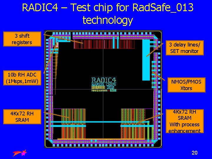
RADIC 4 – Test chip for Rad. Safe_013 technology 3 shift registers 3 delay lines/ SET monitor 10 b RH ADC (1 Msps, 1 m. W) 4 Kx 72 RH SRAM Ramon Chips NMOS/PMOS Xtors 4 Kx 72 RH SRAM With process enhancement 20

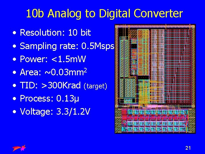
10 b Analog to Digital Converter • • Resolution: 10 bit Sampling rate: 0. 5 Msps Power: <1. 5 m. W Area: ~0. 03 mm 2 TID: >300 Krad (target) Process: 0. 13µ Voltage: 3. 3/1. 2 V Ramon Chips 21

Summary • Rad. Safe™ by Ramon Chips § § § Using standard process Using standard EDA tools & flow Proven Rad-Hard-by-design on several chips Optimized for performance, power & reliability RH considerations applies to all levels of design flow 0. 13µ process provides significant performance advantages Ramon Chips 22