Application specific integrated circuits ASICs Preamplifier design for

- Slides: 1

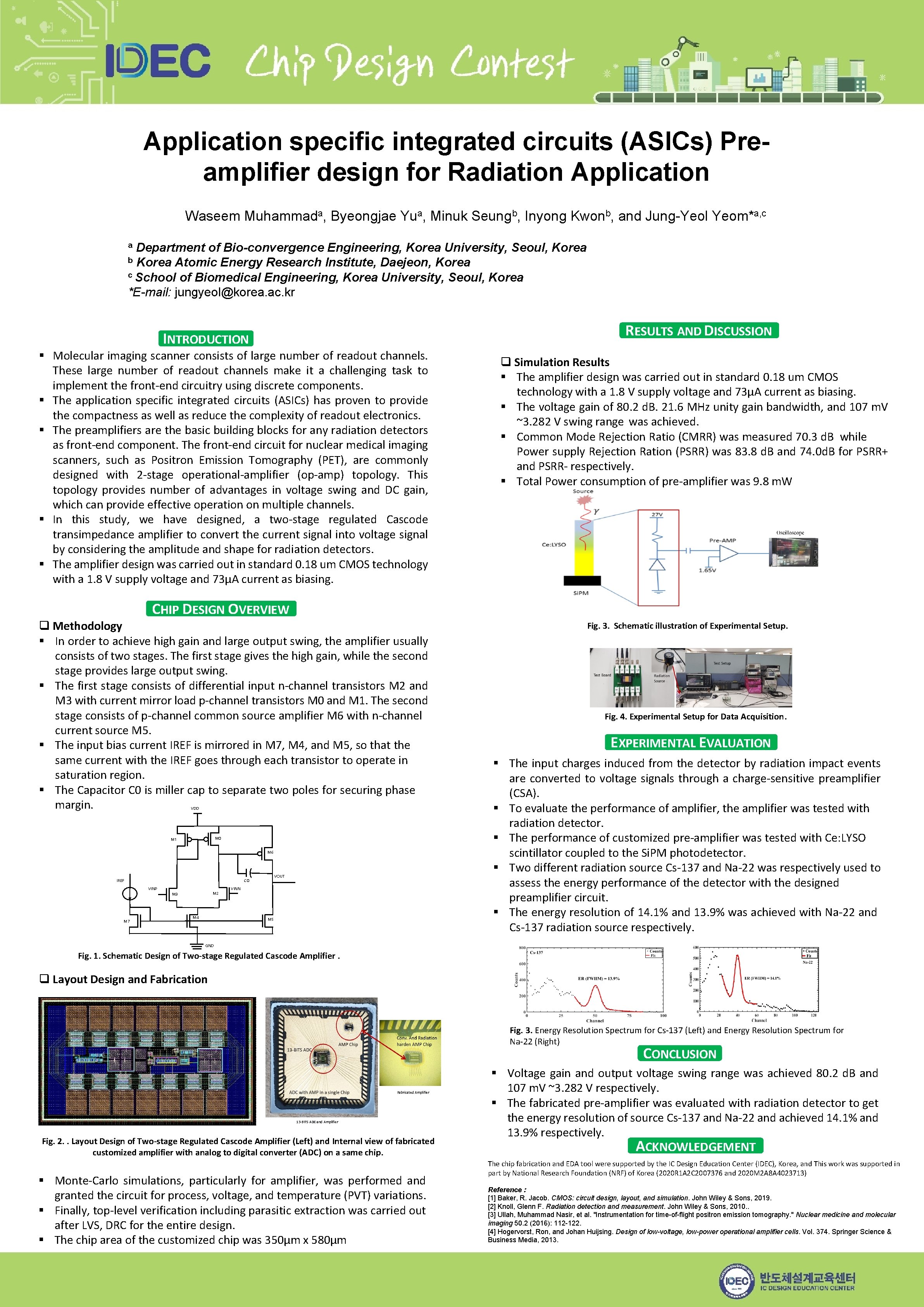
Application specific integrated circuits (ASICs) Preamplifier design for Radiation Application Waseem Muhammada, Byeongjae Yua, Minuk Seungb, Inyong Kwonb, and Jung-Yeol Yeom*a, c Department of Bio-convergence Engineering, Korea University, Seoul, Korea b Korea Atomic Energy Research Institute, Daejeon, Korea c School of Biomedical Engineering, Korea University, Seoul, Korea *E-mail: jungyeol@korea. ac. kr a RESULTS AND DISCUSSION INTRODUCTION § Molecular imaging scanner consists of large number of readout channels. These large number of readout channels make it a challenging task to implement the front-end circuitry using discrete components. § The application specific integrated circuits (ASICs) has proven to provide the compactness as well as reduce the complexity of readout electronics. § The preamplifiers are the basic building blocks for any radiation detectors as front-end component. The front-end circuit for nuclear medical imaging scanners, such as Positron Emission Tomography (PET), are commonly designed with 2 -stage operational-amplifier (op-amp) topology. This topology provides number of advantages in voltage swing and DC gain, which can provide effective operation on multiple channels. § In this study, we have designed, a two-stage regulated Cascode transimpedance amplifier to convert the current signal into voltage signal by considering the amplitude and shape for radiation detectors. § The amplifier design was carried out in standard 0. 18 um CMOS technology with a 1. 8 V supply voltage and 73μA current as biasing. q Simulation Results § The amplifier design was carried out in standard 0. 18 um CMOS technology with a 1. 8 V supply voltage and 73μA current as biasing. § The voltage gain of 80. 2 d. B. 21. 6 MHz unity gain bandwidth, and 107 m. V ~3. 282 V swing range was achieved. § Common Mode Rejection Ratio (CMRR) was measured 70. 3 d. B while Power supply Rejection Ration (PSRR) was 83. 8 d. B and 74. 0 d. B for PSRR+ and PSRR- respectively. § Total Power consumption of pre-amplifier was 9. 8 m. W CHIP DESIGN OVERVIEW q Methodology § In order to achieve high gain and large output swing, the amplifier usually consists of two stages. The first stage gives the high gain, while the second stage provides large output swing. § The first stage consists of differential input n-channel transistors M 2 and M 3 with current mirror load p-channel transistors M 0 and M 1. The second stage consists of p-channel common source amplifier M 6 with n-channel current source M 5. § The input bias current IREF is mirrored in M 7, M 4, and M 5, so that the same current with the IREF goes through each transistor to operate in saturation region. § The Capacitor C 0 is miller cap to separate two poles for securing phase margin. VDD M 0 M 1 M 6 IREF VINP M 2 M 3 M 7 VOUT C 0 M 4 VINN M 5 Fig. 3. Schematic illustration of Experimental Setup. Fig. 4. Experimental Setup for Data Acquisition. EXPERIMENTAL EVALUATION § The input charges induced from the detector by radiation impact events are converted to voltage signals through a charge-sensitive preamplifier (CSA). § To evaluate the performance of amplifier, the amplifier was tested with radiation detector. § The performance of customized pre-amplifier was tested with Ce: LYSO scintillator coupled to the Si. PM photodetector. § Two different radiation source Cs-137 and Na-22 was respectively used to assess the energy performance of the detector with the designed preamplifier circuit. § The energy resolution of 14. 1% and 13. 9% was achieved with Na-22 and Cs-137 radiation source respectively. GND Fig. 1. Schematic Design of Two-stage Regulated Cascode Amplifier. q Layout Design and Fabrication Fig. 3. Energy Resolution Spectrum for Cs-137 (Left) and Energy Resolution Spectrum for Na-22 (Right) CONCLUSION Fabricated Amplifier 13 -BITS ADC and Amplifier Fig. 2. . Layout Design of Two-stage Regulated Cascode Amplifier (Left) and Internal view of fabricated customized amplifier with analog to digital converter (ADC) on a same chip. § Monte-Carlo simulations, particularly for amplifier, was performed and granted the circuit for process, voltage, and temperature (PVT) variations. § Finally, top-level verification including parasitic extraction was carried out after LVS, DRC for the entire design. § The chip area of the customized chip was 350μm x 580μm § Voltage gain and output voltage swing range was achieved 80. 2 d. B and 107 m. V ~3. 282 V respectively. § The fabricated pre-amplifier was evaluated with radiation detector to get the energy resolution of source Cs-137 and Na-22 and achieved 14. 1% and 13. 9% respectively. ACKNOWLEDGEMENT The chip fabrication and EDA tool were supported by the IC Design Education Center (IDEC), Korea, and This work was supported in part by National Research Foundation (NRF) of Korea (2020 R 1 A 2 C 2007376 and 2020 M 2 A 8 A 4023713) Reference : [1] Baker, R. Jacob. CMOS: circuit design, layout, and simulation. John Wiley & Sons, 2019. [2] Knoll, Glenn F. Radiation detection and measurement. John Wiley & Sons, 2010. . [3] Ullah, Muhammad Nasir, et al. "Instrumentation for time-of-flight positron emission tomography. " Nuclear medicine and molecular imaging 50. 2 (2016): 112 -122. [4] Hogervorst, Ron, and Johan Huijsing. Design of low-voltage, low-power operational amplifier cells. Vol. 374. Springer Science & Business Media, 2013.