Practical PhaseLocked Loop Design 2004 ISSCC Tutorial Dennis
![Paper References [1] B. Razavi, Monolithic Phase-Locked Loops and Clock-Recovery Circuits, IEEE Press, 1996. Paper References [1] B. Razavi, Monolithic Phase-Locked Loops and Clock-Recovery Circuits, IEEE Press, 1996.](https://slidetodoc.com/presentation_image/49fd03bf46a598ba555ccafd48606513/image-128.jpg)
![Paper References (cont. ) [7] I. Young, “A 0. 35 um CMOS 3 -880 Paper References (cont. ) [7] I. Young, “A 0. 35 um CMOS 3 -880](https://slidetodoc.com/presentation_image/49fd03bf46a598ba555ccafd48606513/image-129.jpg)
![Paper References (cont. ) [7] A. Maxim, “A 160 -2550 MHz CMOS Active Clock Paper References (cont. ) [7] A. Maxim, “A 160 -2550 MHz CMOS Active Clock](https://slidetodoc.com/presentation_image/49fd03bf46a598ba555ccafd48606513/image-130.jpg)
![Monograph References [1] B. Razavi, Design of Analog CMOS Integrated Circuits, Mc. Graw-Hill, 2001. Monograph References [1] B. Razavi, Design of Analog CMOS Integrated Circuits, Mc. Graw-Hill, 2001.](https://slidetodoc.com/presentation_image/49fd03bf46a598ba555ccafd48606513/image-131.jpg)
- Slides: 131

Practical Phase-Locked Loop Design 2004 ISSCC Tutorial Dennis Fischette Email: pll@delroy. com Website: http: //www. delroy. com/pll Copyright, Dennis Fischette, 2004 1

Outline • Introduction • Basic Feedback Loop Theory • Circuits • “Spectacular” Failures • Appendices: – design for test – writing a PLL Spec – references • Sorry: no DLL’s in this tutorial Copyright, Dennis Fischette, 2004 2

Intended Audience • If you… • Are a novice PLL designer • Specify PLL requirements • Integrate PLL’s on-chip • Test/debug PLL’s • Review PLL designs Copyright, Dennis Fischette, 2004 3

Introduction Copyright, Dennis Fischette, 2004 4

What is a PLL? • A PLL is a negative feedback system where an oscillator-generated signal is phase and frequency locked to a reference signal. • Analogous to a car’s “cruise control” Copyright, Dennis Fischette, 2004 5

How are PLL’s Used? • Frequency Synthesis (e. g. generating a 1 GHz clock from a 100 MHz reference) • Skew Cancellation (e. g. phase-aligning an internal clock to the IO clock) (May use a DLL instead) • Extracting a clock from a random data stream (e. g. serial-link receiver) • Frequency Synthesis is the focus of this tutorial. Copyright, Dennis Fischette, 2004 6

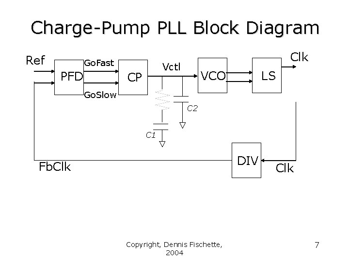
Charge-Pump PLL Block Diagram Ref Go. Fast PFD Clk Vctl CP VCO LS Go. Slow C 2 C 1 DIV Fb. Clk Copyright, Dennis Fischette, 2004 Clk 7

Charge-Pump PLL Building Blocks • Phase-Frequency Detector (PFD) • Charge-Pump (CP) • Low-Pass Filter (LPF) • Voltage-Controlled Oscillator (VCO) • VCO Level-Shifter (LS) • Feedback Divider (FBDIV) • Power Supply regulator/filter (VREG)? Copyright, Dennis Fischette, 2004 8

Components in a Nutshell • PFD: outputs digital pulse whose width is proportional to phase error • CP: converts digital error pulse to analog error current • LPF: integrates (and low-pass filters) error current to generate VCO control voltage • VCO: low-swing oscillator with frequency proportional to control voltage • LS: amplifies VCO levels to full-swing • DIV: divides VCO clock to generate FBCLK clock Copyright, Dennis Fischette, 2004 9

PLL Feedback Loop Theory Copyright, Dennis Fischette, 2004 10

Is My PLL Stable? • PLL is 2 nd-order system similar to mass-springdashpot or RLC circuit. • PLL may be stable or unstable depending on phase margin (or damping factor). • Phase margin is determined from linear model of PLL in frequency-domain. • Find phase margin/damping using MATLAB, loop equations, or simulations. • Stability affects phase error, settling, jitter. Copyright, Dennis Fischette, 2004 11

What Does PLL Bandwidth Mean? • PLL acts as a low-pass filter with respect to the reference. • Low-frequency reference modulation (e. g. spreadspectrum clocking) is passed to the VCO clock. • High-frequency reference jitter is rejected. • “Bandwidth” is the frequency at which the PLL begins to lose lock with the reference (-3 d. B). • PLL acts as a high-pass filter wrt VCO noise. • Bandwidth affects phase error, settling, jitter. Copyright, Dennis Fischette, 2004 12

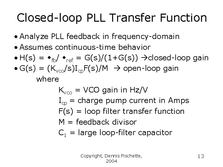
Closed-loop PLL Transfer Function • Analyze PLL feedback in frequency-domain • Assumes continuous-time behavior • H(s) = fb/ ref = G(s)/(1+G(s)) closed-loop gain • G(s) = (Kvco/s)Icp. F(s)/M open-loop gain where Kvco = VCO gain in Hz/V Icp = charge pump current in Amps F(s) = loop filter transfer function M = feedback divisor C 1 = large loop-filter capacitor Copyright, Dennis Fischette, 2004 13

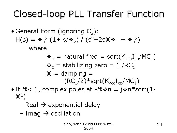
Closed-loop PLL Transfer Function • General Form (ignoring C 2): H(s) = n 2 (1+ s/ z) / (s 2+2 s n + n 2) where n = natural freq = sqrt(Kvco. Icp/MC 1) z = stabilizing zero = 1 /RC 1 = damping = (RC 1/2)*sqrt(Kvco. Icp/MC 1) • If < 1, complex poles at - n ± j n*sqrt(1 - 2 ) – Real exponential delay – Imag oscillation Copyright, Dennis Fischette, 2004 14

What Determines Stability and Bandwidth? • Damping Factor (measure of stability) • Natural Frequency (measure of bandwidth) • Damping and natural frequency can be set independently by LPF resistor Copyright, Dennis Fischette, 2004 15

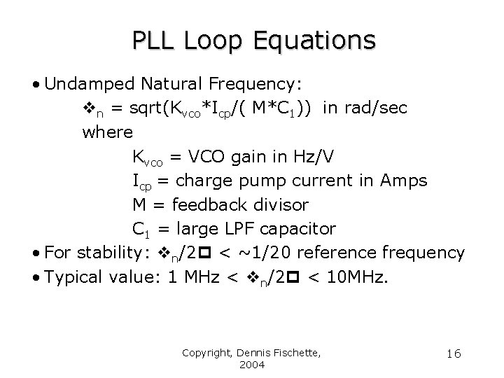
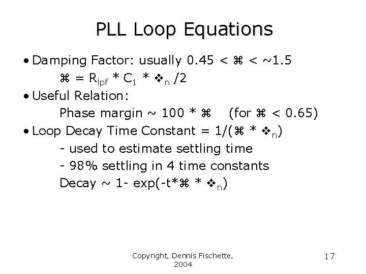
PLL Loop Equations • Undamped Natural Frequency: n = sqrt(Kvco*Icp/( M*C 1)) in rad/sec where Kvco = VCO gain in Hz/V Icp = charge pump current in Amps M = feedback divisor C 1 = large LPF capacitor • For stability: n/2 < ~1/20 reference frequency • Typical value: 1 MHz < n/2 < 10 MHz. Copyright, Dennis Fischette, 2004 16

PLL Loop Equations • Damping Factor: usually 0. 45 < < ~1. 5 = Rlpf * C 1 * n /2 • Useful Relation: Phase margin ~ 100 * (for < 0. 65) • Loop Decay Time Constant = 1/( * n) - used to estimate settling time - 98% settling in 4 time constants Decay ~ 1 - exp(-t* * n) Copyright, Dennis Fischette, 2004 17

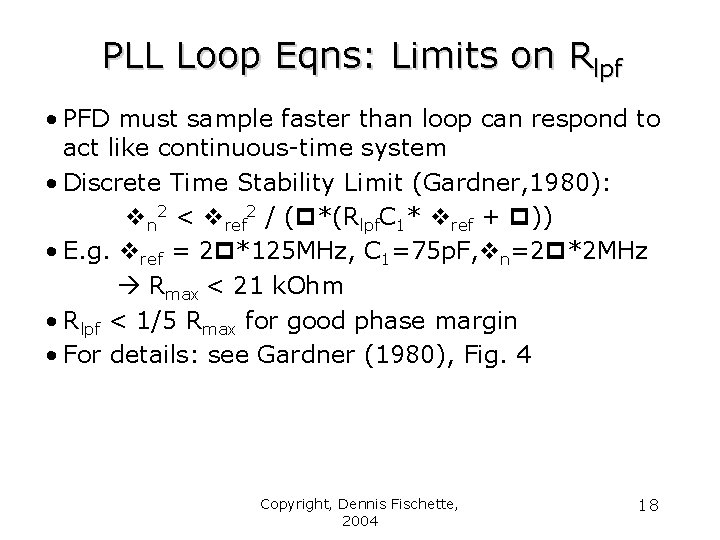
PLL Loop Eqns: Limits on Rlpf • PFD must sample faster than loop can respond to act like continuous-time system • Discrete Time Stability Limit (Gardner, 1980): n 2 < ref 2 / ( *(Rlpf. C 1* ref + )) • E. g. ref = 2 *125 MHz, C 1=75 p. F, n=2 *2 MHz Rmax < 21 k. Ohm • Rlpf < 1/5 Rmax for good phase margin • For details: see Gardner (1980), Fig. 4 Copyright, Dennis Fischette, 2004 18

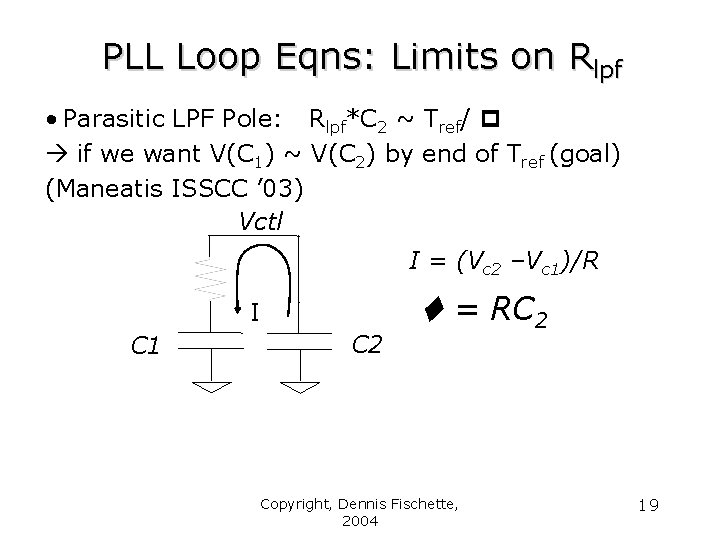
PLL Loop Eqns: Limits on Rlpf • Parasitic LPF Pole: Rlpf*C 2 ~ Tref/ if we want V(C 1) ~ V(C 2) by end of Tref (goal) (Maneatis ISSCC ’ 03) Vctl I = (Vc 2 –Vc 1)/R I C 1 C 2 = RC 2 Copyright, Dennis Fischette, 2004 19

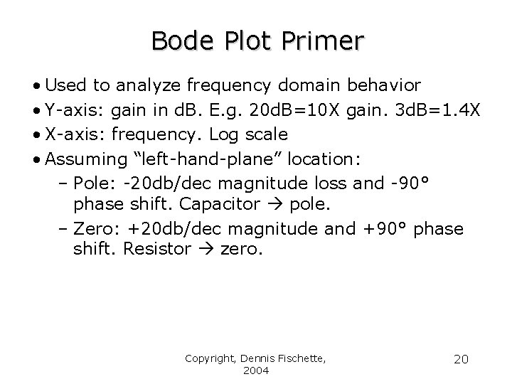
Bode Plot Primer • Used to analyze frequency domain behavior • Y-axis: gain in d. B. E. g. 20 d. B=10 X gain. 3 d. B=1. 4 X • X-axis: frequency. Log scale • Assuming “left-hand-plane” location: – Pole: -20 db/dec magnitude loss and -90° phase shift. Capacitor pole. – Zero: +20 db/dec magnitude and +90° phase shift. Resistor zero. Copyright, Dennis Fischette, 2004 20

PLL Response vs. Damping Copyright, Dennis Fischette, 2004 21

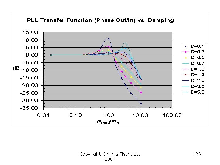
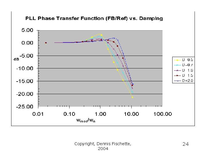
Phase Tracking vs. Damping • Peaking at low and high damping factors bad • Damping ~ 1 good compromise • Phase Tracking think “accumulated” jitter or phase error • VCO frequency peaking (aka period jitter) similar to phase peaking Copyright, Dennis Fischette, 2004 22

Copyright, Dennis Fischette, 2004 23

Copyright, Dennis Fischette, 2004 24

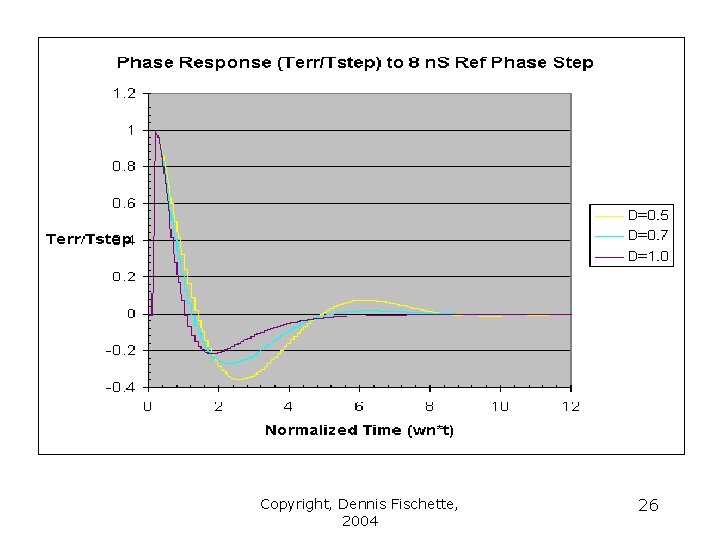
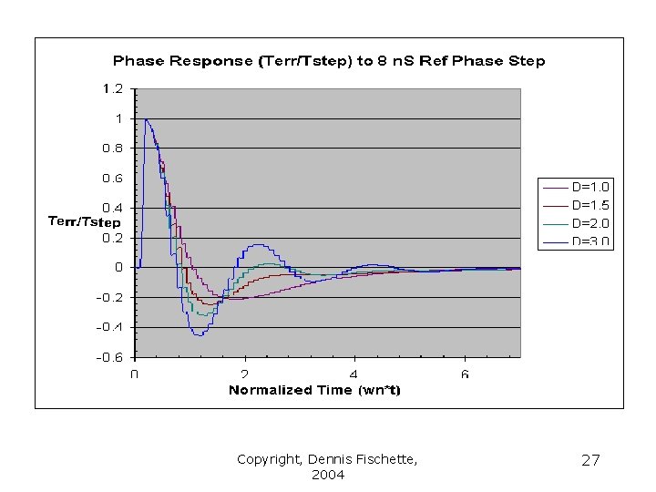
Transient: Phase Error vs. Damping • Less ringing and overshoot as 1 • Severe overdamping ringing and overshoot • Ringing at high damping due to low oversampling (large R) – Gardner limit. Copyright, Dennis Fischette, 2004 25

Copyright, Dennis Fischette, 2004 26

Copyright, Dennis Fischette, 2004 27

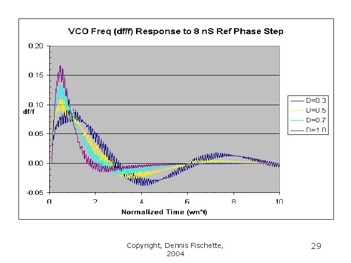
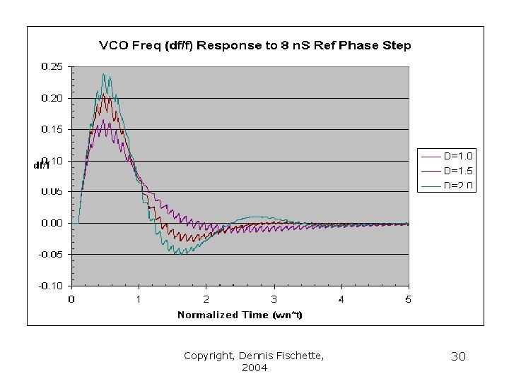
VCO Jitter (df/f) vs. Damping • Low damping less period jitter, slower response, more phase error • High damping low oversampling (large R) causes oscillation Copyright, Dennis Fischette, 2004 28

Copyright, Dennis Fischette, 2004 29

Copyright, Dennis Fischette, 2004 30

PLL Response vs. Bandwidth Copyright, Dennis Fischette, 2004 31

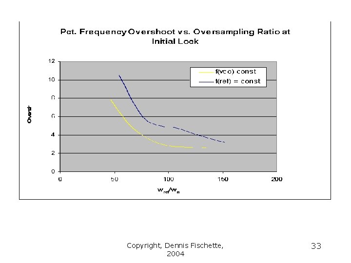
VCO Freq. Overshoot vs. Bandwidth • Lower BW lower overshoot • Higher Over. Sampling. Ratio ( ref/ n) lower bandwidth(BW) • Note: ~ BW in these simulations Copyright, Dennis Fischette, 2004 32

Copyright, Dennis Fischette, 2004 33

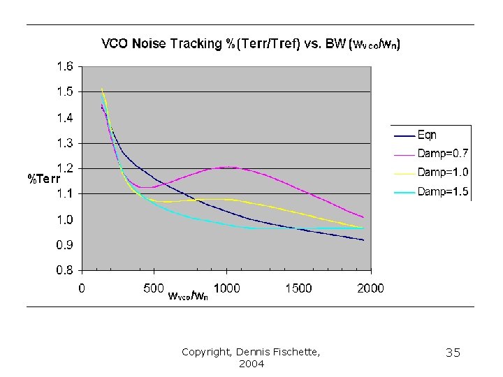
Phase Error (due to VCO Noise) vs. BW • For random VCO noise (I. e. thermal): lower BW higher accumulated phase error • Why? More jittery VCO cycles before PLL starts to correct: Terr ~ Jrms * sqrt(2 fvco/ n) where Jrms = std dev of VCO period jitter - valid for damping ~ 1 - assume: Jrms ~ 1/fvco higher f, lower Jrms Copyright, Dennis Fischette, 2004 34

Copyright, Dennis Fischette, 2004 35

PLL Circuits • Phase-Frequency Detector • Charge-Pump • Low-Pass Filter • Voltage-Controlled Oscillator • Level-Shifter • Voltage Regulator Copyright, Dennis Fischette, 2004 36

Phase-Frequency Detector(PFD) Copyright, Dennis Fischette, 2004 37

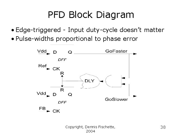
PFD Block Diagram • Edge-triggered - Input duty-cycle doesn’t matter • Pulse-widths proportional to phase error Copyright, Dennis Fischette, 2004 38

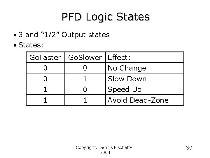
PFD Logic States • 3 and “ 1/2” Output states • States: Go. Faster Go. Slower Effect: 0 0 No Change 0 1 Slow Down 1 0 Speed Up 1 1 Avoid Dead-Zone Copyright, Dennis Fischette, 2004 39

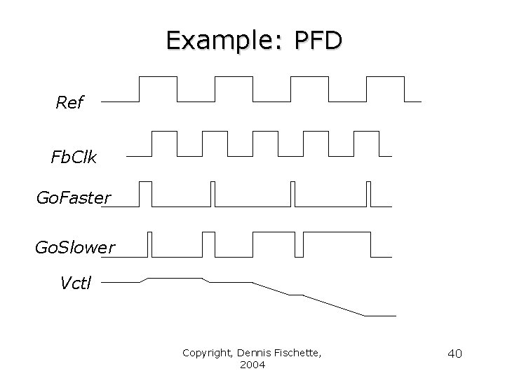
Example: PFD Ref Fb. Clk Go. Faster Go. Slower Vctl Copyright, Dennis Fischette, 2004 40

Avoiding the Dead-Zone • “Dead-zone” occurs when the loop doesn’t respond to small phase errors - e. g. 10 p. S phase error at PFD inputs: – PFD cannot generate 10 p. S wide Go. Faster and Go. Slower pulses – Charge-pump switches cannot turn on and off in 10 p. S – Solution: delay reset to guarantee min. pulse width (typically > 150 p. S) Copyright, Dennis Fischette, 2004 41

Charge Pump(CP) Copyright, Dennis Fischette, 2004 42

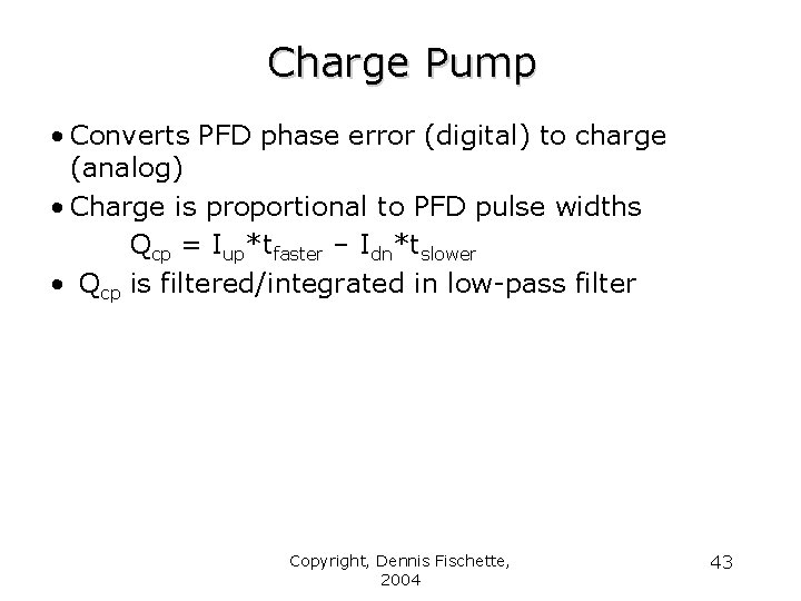
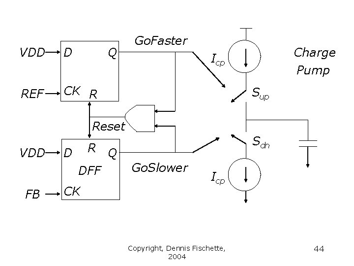
Charge Pump • Converts PFD phase error (digital) to charge (analog) • Charge is proportional to PFD pulse widths Qcp = Iup*tfaster – Idn*tslower • Qcp is filtered/integrated in low-pass filter Copyright, Dennis Fischette, 2004 43

VDD D Q REF CK R Go. Faster Charge Pump Icp Sup Reset VDD R D DFF FB CK Sdn Q Go. Slower Icp Copyright, Dennis Fischette, 2004 44

Charge-Pump Wish List • Equal UP/DOWN currents over entire control voltage range - reduce phase error. • Minimal coupling to control voltage during switching - reduce jitter. • Insensitive to power-supply noise and process variations – loop stability. • Easy-to-design, PVT-insensitive reference current. • Programmable currents to maintain loop dynamics (vs. M, fref)? • Typical: 1 A (mismatch)< Icp < 50 A ( Vctl) Copyright, Dennis Fischette, 2004 45

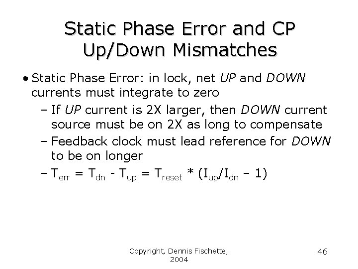
Static Phase Error and CP Up/Down Mismatches • Static Phase Error: in lock, net UP and DOWN currents must integrate to zero – If UP current is 2 X larger, then DOWN current source must be on 2 X as long to compensate – Feedback clock must lead reference for DOWN to be on longer – Terr = Tdn - Tup = Treset * (Iup/Idn – 1) Copyright, Dennis Fischette, 2004 46

Static Phase Error and CP Up/Down Mismatches • Phase error can be extremely large at low VCO frequencies (esp. if self-biased) due to mismatch in current mirrors (low Vgs-Vt) • Increase Vgs or decrease Vt (large W*L) • Typical static phase error < 100 p. S Copyright, Dennis Fischette, 2004 47

VCO Jitter and CP Up/Down Mismatches • PFD-CP correct at rate of reference (e. g. 10 n. S). • Most phase error correction occurs near reference rising edge and lasts < 200 p. S, causing a control voltage ripple. • This ripple affects the VCO cycles near the reference more than VCO cycles later in the ref cycle, causing VCO jitter. • Typ. Jitter << 1% due to Up/Down Mismatches • Avoid ripple by spreading correction over entire ref cycle. (Maneatis JSSC ’ 03) Copyright, Dennis Fischette, 2004 48

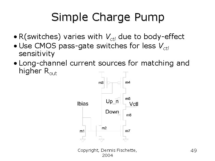
Simple Charge Pump • R(switches) varies with Vctl due to body-effect • Use CMOS pass-gate switches for less Vctl sensitivity • Long-channel current sources for matching and higher Rout Copyright, Dennis Fischette, 2004 49

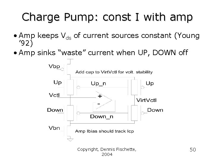
Charge Pump: const I with amp • Amp keeps Vds of current sources constant (Young ’ 92) • Amp sinks “waste” current when UP, DOWN off Copyright, Dennis Fischette, 2004 50

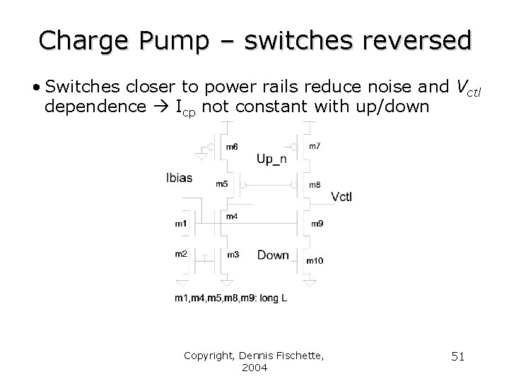
Charge Pump – switches reversed • Switches closer to power rails reduce noise and Vctl dependence Icp not constant with up/down Copyright, Dennis Fischette, 2004 51

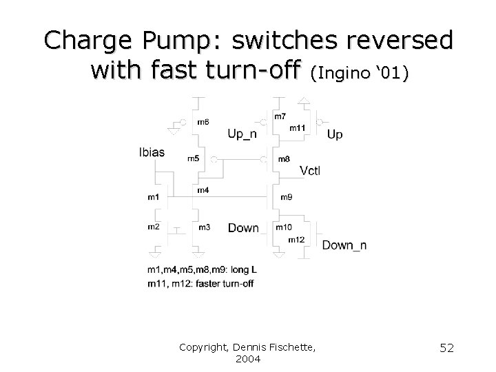
Charge Pump: switches reversed with fast turn-off (Ingino ‘ 01) Copyright, Dennis Fischette, 2004 52

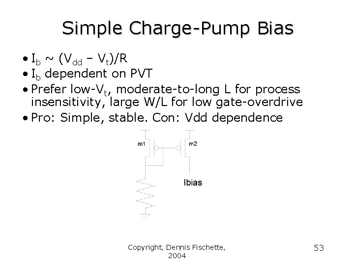
Simple Charge-Pump Bias • Ib ~ (Vdd – Vt)/R • Ib dependent on PVT • Prefer low-Vt, moderate-to-long L for process insensitivity, large W/L for low gate-overdrive • Pro: Simple, stable. Con: Vdd dependence Copyright, Dennis Fischette, 2004 53

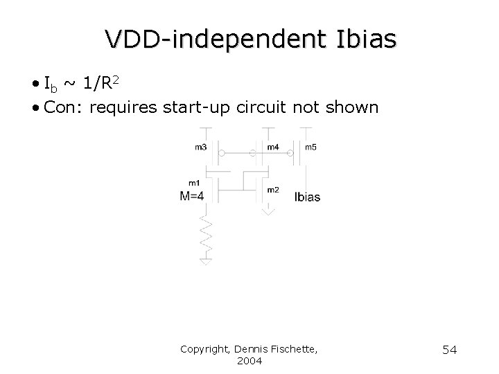
VDD-independent Ibias • Ib ~ 1/R 2 • Con: requires start-up circuit not shown Copyright, Dennis Fischette, 2004 54

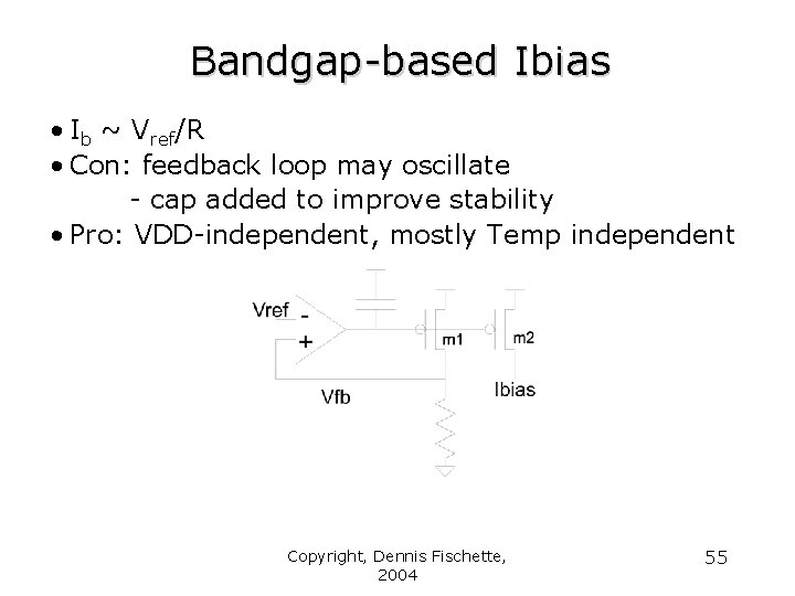
Bandgap-based Ibias • Ib ~ Vref/R • Con: feedback loop may oscillate - cap added to improve stability • Pro: VDD-independent, mostly Temp independent Copyright, Dennis Fischette, 2004 55

Low-Pass Filter (LPF) Copyright, Dennis Fischette, 2004 56

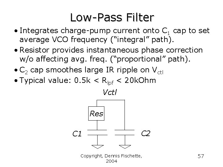
Low-Pass Filter • Integrates charge-pump current onto C 1 cap to set average VCO frequency (“integral” path). • Resistor provides instantaneous phase correction w/o affecting avg. freq. (“proportional” path). • C 2 cap smoothes large IR ripple on Vctl • Typical value: 0. 5 k < Rlpf < 20 k. Ohm Vctl Res C 1 C 2 Copyright, Dennis Fischette, 2004 57

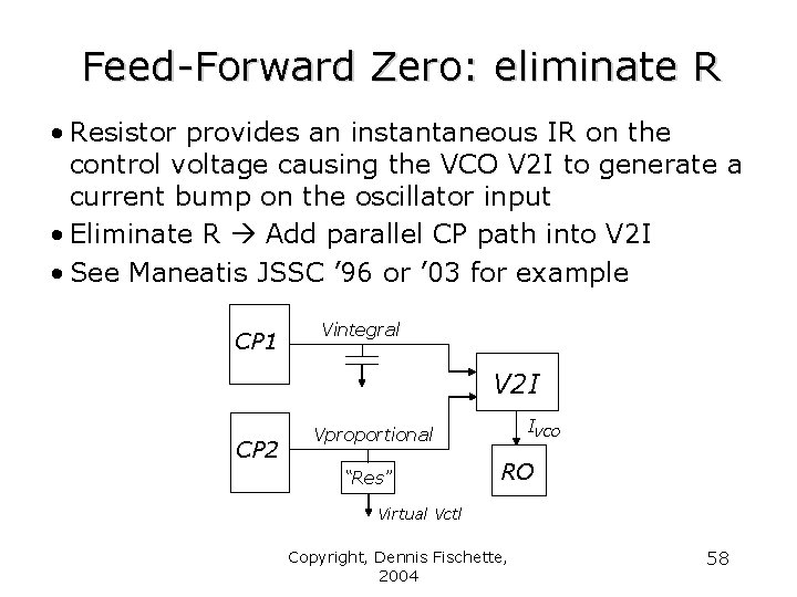
Feed-Forward Zero: eliminate R • Resistor provides an instantaneous IR on the control voltage causing the VCO V 2 I to generate a current bump on the oscillator input • Eliminate R Add parallel CP path into V 2 I • See Maneatis JSSC ’ 96 or ’ 03 for example CP 1 Vintegral V 2 I CP 2 IVCO Vproportional “Res” RO Virtual Vctl Copyright, Dennis Fischette, 2004 58

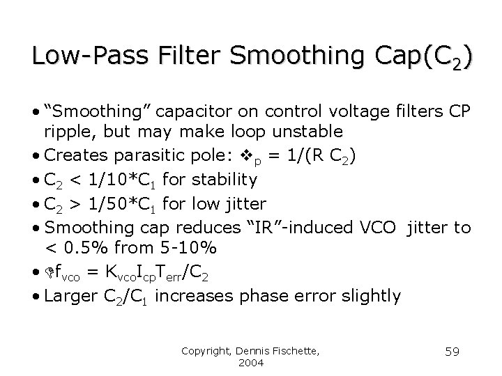
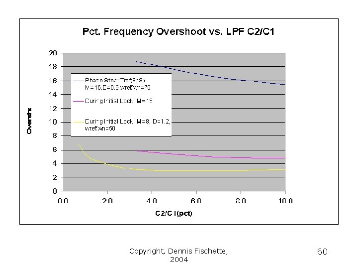
Low-Pass Filter Smoothing Cap(C 2) • “Smoothing” capacitor on control voltage filters CP ripple, but may make loop unstable • Creates parasitic pole: p = 1/(R C 2) • C 2 < 1/10*C 1 for stability • C 2 > 1/50*C 1 for low jitter • Smoothing cap reduces “IR”-induced VCO jitter to < 0. 5% from 5 -10% • fvco = Kvco. Icp. Terr/C 2 • Larger C 2/C 1 increases phase error slightly Copyright, Dennis Fischette, 2004 59

Copyright, Dennis Fischette, 2004 60

Low-Pass Filter Capacitors • At <= 130 nm, thin-gate oxide leakage is huge: – Ileak ~ Vgate 4. 5 – NMOS leakier than PMOS – Weak temperature dependence – Ileak vs. tox ~2 -3 X per Angstrom • Use metal caps or thick-gate oxide caps to reduce leakage • Metal caps use 10 X more area than thin gate caps – Use minimum width/spacing parallel lines – Hard to LVS - Check extracted layout for correct connectivity Copyright, Dennis Fischette, 2004 61

Low-Pass Filter Capacitors • Even thick gate oxide may still leak too much • Large filter cap (C 1) typically ranges from 50 p. F to 400 p. F • C 1 cap BW may be low as ~10 X PLL BW for nearly ideal behavior • Min C 2 BW set by Tref • Cap BW ~ 1/RC ~ 1/L 2 • Gate cap not constant with Vgs Copyright, Dennis Fischette, 2004 62

Voltage-Controlled Oscillator (VCO) Copyright, Dennis Fischette, 2004 63

Voltage-Controlled Oscillator • VCO usually consists of two parts: control voltage- to-control current (V 2 I) circuit and currentcontrolled ring oscillator (ICO) • VCO may be single-ended or differential • Differential design allows for even number of oscillator stages if differential-pair amps used for delay cells • V 2 V may be used instead to generate bias voltages for diff-pair amps Copyright, Dennis Fischette, 2004 64

PLL Suppression of VCO Noise • PLL acts like a high-pass filter in allowing VCO noise to reach PLL output • Need noise-immune VCO to minimize jitter – Feedback loop cannot react quickly. • Power-supply noise is largest source of VCO noise Copyright, Dennis Fischette, 2004 65

VCO Design Concerns • Min low-frequency power-supply sensitivity < 0. 05% per %d. VDD reduce phase error • Min high-frequency power-supply sensitivity < 0. 1% per %d. VDD reduce period jitter Note: this is 10 X better than normal INV • Low substrate-noise sensitivity reduce Vt – unnecessary in SOI • Thermal noise (k. T) – typically < 1% VCO period at high frequency Copyright, Dennis Fischette, 2004 66

VCO Design Concerns • Large frequency range to cover PVT variation: 3 -5 X typical • Single-ended or differential? – use differential for 50% duty-cycle • Vco gain (fvco = Kvco* Vctl) affects loop stability • Typical VCO gain: Kvco ~ 1 -3 X * fmax • More delay stages easier to initiate oscillation – Gain(DC) > 2 for 3 stages – Gain(DC) > sqrt(2) for 4 stages Copyright, Dennis Fischette, 2004 67

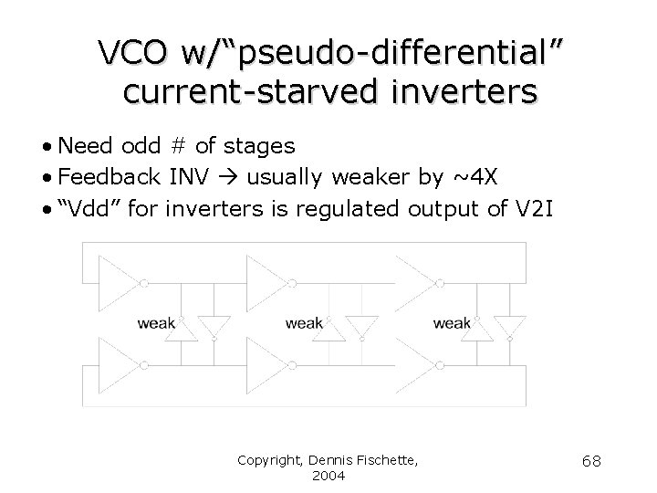
VCO w/“pseudo-differential” current-starved inverters • Need odd # of stages • Feedback INV usually weaker by ~4 X • “Vdd” for inverters is regulated output of V 2 I Copyright, Dennis Fischette, 2004 68

VCO V-to-I Circuits • Converts Vctl to Ictl • May generate additional Vbias for oscillator • May use internal feedback to set VCO swing • Provides power-supply rejection fets in deep saturation or amp-based internal feedback • Filters high-frequency Vctl ripple w/another cap • Adds parasitic pole BW(V 2 I) >> BW(PLL) • Digital Range settings allow for control of VCO gain and Vctl range must overlap ranges Copyright, Dennis Fischette, 2004 69

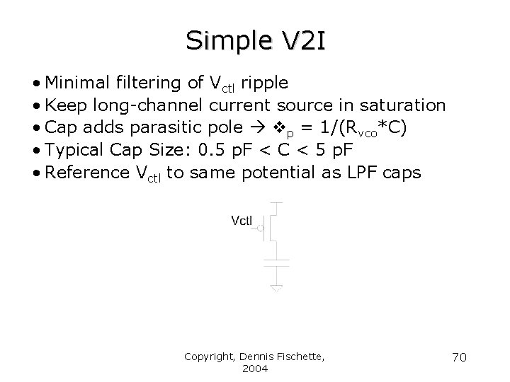
Simple V 2 I • Minimal filtering of Vctl ripple • Keep long-channel current source in saturation • Cap adds parasitic pole p = 1/(Rvco*C) • Typical Cap Size: 0. 5 p. F < C < 5 p. F • Reference Vctl to same potential as LPF caps Copyright, Dennis Fischette, 2004 70

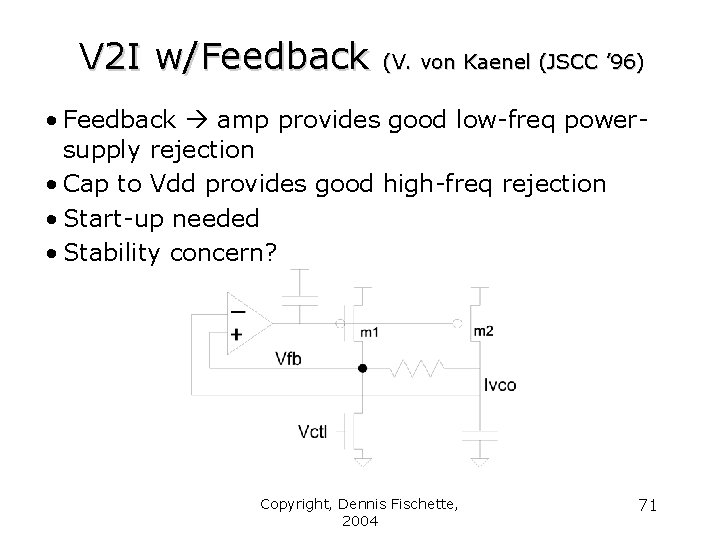
V 2 I w/Feedback (V. von Kaenel (JSCC ’ 96) • Feedback amp provides good low-freq powersupply rejection • Cap to Vdd provides good high-freq rejection • Start-up needed • Stability concern? Copyright, Dennis Fischette, 2004 71

Differential VCO’s Copyright, Dennis Fischette, 2004 72

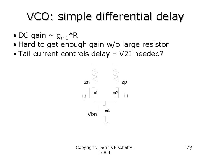
VCO: simple differential delay • DC gain ~ gm 1*R • Hard to get enough gain w/o large resistor • Tail current controls delay – V 2 I needed? Copyright, Dennis Fischette, 2004 73

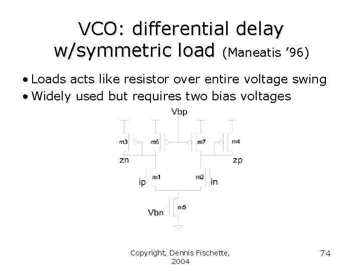
VCO: differential delay w/symmetric load (Maneatis ’ 96) • Loads acts like resistor over entire voltage swing • Widely used but requires two bias voltages Copyright, Dennis Fischette, 2004 74

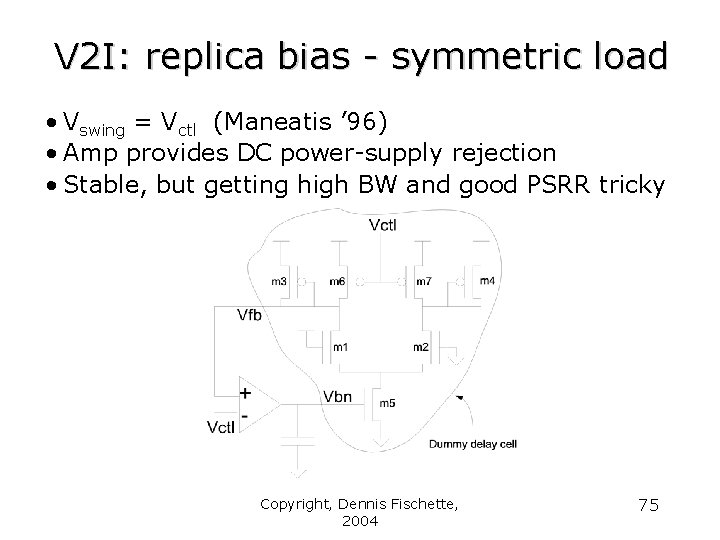
V 2 I: replica bias - symmetric load • Vswing = Vctl (Maneatis ’ 96) • Amp provides DC power-supply rejection • Stable, but getting high BW and good PSRR tricky Copyright, Dennis Fischette, 2004 75

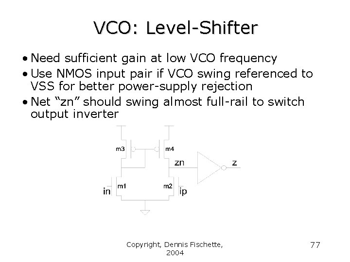
VCO Level-Shifter • Amplify limited-swing VCO signals to full-rail – typically from 0. 4 -0. 7 V to VDD • Maintain 50% duty-cycle – usually +/- 3% – difficult to do over PVT and frequency • Insensitive to power-supply noise < 0. 5 % per % d. VDD • Which power-supply? Analog or digital? – usually digital Copyright, Dennis Fischette, 2004 76

VCO: Level-Shifter • Need sufficient gain at low VCO frequency • Use NMOS input pair if VCO swing referenced to VSS for better power-supply rejection • Net “zn” should swing almost full-rail to switch output inverter Copyright, Dennis Fischette, 2004 77

Feedback Divider Copyright, Dennis Fischette, 2004 78

Feedback Divider (FBDIV) • Divide VCO by N fref = fvco/N • Divider may be internal to PLL or after CPU clock tree • Max FBDIV frequency should be greater than max VCO frequency to avoid “run-away” • Minimize FBDIV latency to reduce VDD-induced jitter seen at phase detector • Loop Phase Margin Degradation ~ n. Tdly – usually insignificant Copyright, Dennis Fischette, 2004 79

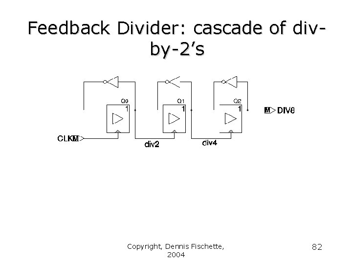
Feedback Divider • Two common types of dividers: – Asynchronous cascade of div-by-2’s – Synchronous counter – typically used Copyright, Dennis Fischette, 2004 80

Asynchronous Divide-by-2 • Pro: fast, simple • Pro: small area • Con: long latency for large divisors • Con: divide by powers of 2 only • Can be used as front-end to synchronous counter divider to reduce speed requirements Copyright, Dennis Fischette, 2004 81

Feedback Divider: cascade of divby-2’s Copyright, Dennis Fischette, 2004 82

Counter-Based Divider • Pro: divide by any integer N • Pro: constant latency vs. N • Pro: low latency • Pro: small area Binary-encoded. • Con: slow if using ripple counter don’t • Con: output may glitch delay (re-sample) output by one cycle to clean up glitch Copyright, Dennis Fischette, 2004 83

VDDA Voltage Regulator Copyright, Dennis Fischette, 2004 84

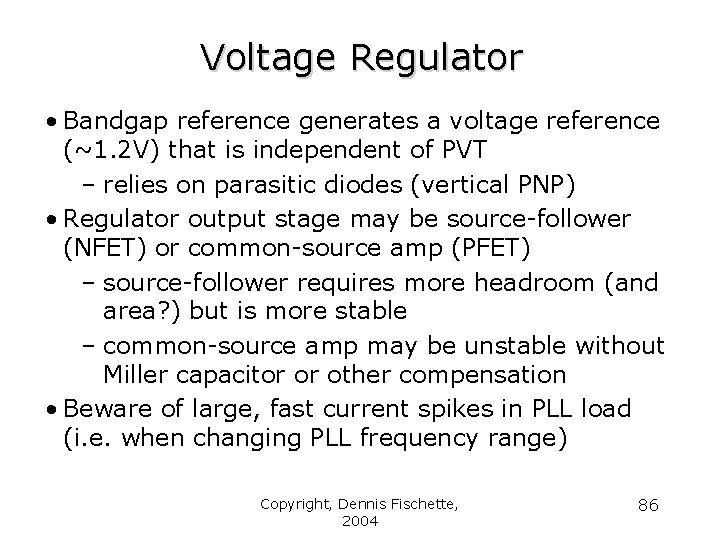
Voltage Regulator/Filter • Used to filter power-supply noise – typically > 20 d. B (10 x) PSRR over entire frequency range – desire 30+ d. B • Secondary purpose is to set precise voltage level for PLL power supply – usually set by bandgap reference Copyright, Dennis Fischette, 2004 85

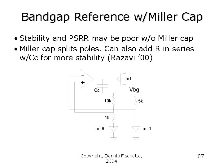
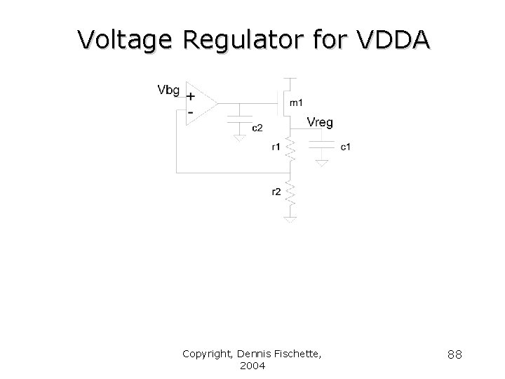
Voltage Regulator • Bandgap reference generates a voltage reference (~1. 2 V) that is independent of PVT – relies on parasitic diodes (vertical PNP) • Regulator output stage may be source-follower (NFET) or common-source amp (PFET) – source-follower requires more headroom (and area? ) but is more stable – common-source amp may be unstable without Miller capacitor or other compensation • Beware of large, fast current spikes in PLL load (i. e. when changing PLL frequency range) Copyright, Dennis Fischette, 2004 86

Bandgap Reference w/Miller Cap • Stability and PSRR may be poor w/o Miller cap • Miller cap splits poles. Can also add R in series w/Cc for more stability (Razavi ’ 00) Copyright, Dennis Fischette, 2004 87

Voltage Regulator for VDDA Copyright, Dennis Fischette, 2004 88

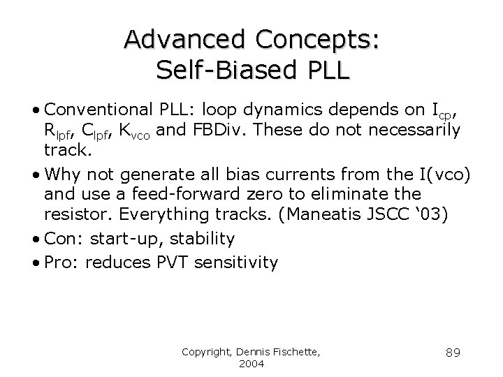
Advanced Concepts: Self-Biased PLL • Conventional PLL: loop dynamics depends on Icp, Rlpf, Clpf, Kvco and FBDiv. These do not necessarily track. • Why not generate all bias currents from the I(vco) and use a feed-forward zero to eliminate the resistor. Everything tracks. (Maneatis JSCC ‘ 03) • Con: start-up, stability • Pro: reduces PVT sensitivity Copyright, Dennis Fischette, 2004 89

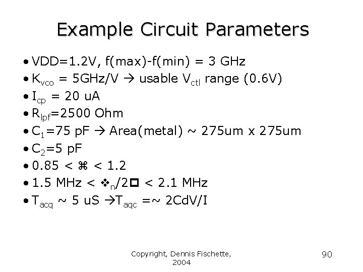
Example Circuit Parameters • VDD=1. 2 V, f(max)-f(min) = 3 GHz • Kvco = 5 GHz/V usable Vctl range (0. 6 V) • Icp = 20 u. A • Rlpf=2500 Ohm • C 1=75 p. F Area(metal) ~ 275 um x 275 um • C 2=5 p. F • 0. 85 < < 1. 2 • 1. 5 MHz < n/2 < 2. 1 MHz • Tacq ~ 5 u. S Taqc =~ 2 Cd. V/I Copyright, Dennis Fischette, 2004 90

Real-world PLL Failures Copyright, Dennis Fischette, 2004 91

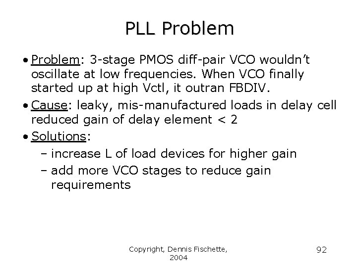
PLL Problem • Problem: 3 -stage PMOS diff-pair VCO wouldn’t oscillate at low frequencies. When VCO finally started up at high Vctl, it outran FBDIV. • Cause: leaky, mis-manufactured loads in delay cell reduced gain of delay element < 2 • Solutions: – increase L of load devices for higher gain – add more VCO stages to reduce gain requirements Copyright, Dennis Fischette, 2004 92

PLL Problem • Problem: VCO stuck at max frequency at power-on. • Cause: PLL tried to lock before VDD was stable. Because VCO couldn’t run fast enough to lock at low VDD, Vctl saturated. When VDD finally stabilized, Vctl = VDD, causing a maxed-out VCO to outrun FBDIV. • Solution: maintain PLL RESET high until VDD is stable to keep Vctl at 0 V. Copyright, Dennis Fischette, 2004 93

PLL Problem • Problem: VCO stuck at max frequency after changing power-modes. • Cause: Feedback DIV could not run fast enough to handle VCO overshoot when locking to a new frequency or facing a reference phase step. • Solutions: – limit size of frequency steps – increase speed of Feedback DIV Copyright, Dennis Fischette, 2004 94

PLL Problem • Problem: PLL would not lock. • Cause: Feedback DIV generated glitches causing PFD to get confused. • Solution: add re-sampling flop to output of feedback DIV to remove glitches. Copyright, Dennis Fischette, 2004 95

PLL Problem • Problem: PLL output clock occasionally skipped edges at low VCO frequencies • Cause: VCO level-shifter had insufficient gain when VCO swing was close to Vt. • Solutions: – increase W of diff-pair inputs – use low-Vt devices Copyright, Dennis Fischette, 2004 96

PLL Problem • Problem: VCO jitter was huge at some divider settings and fine at others. • Cause: Integration team connected programmable current sources backward. • Solution: write accurate verilog model that complains when inputs are out-of-range. Copyright, Dennis Fischette, 2004 97

PLL Problem • Problem: PLL jitter was poor at low freq and good at high freq. • Cause: Vctl was too close to Vt at low frequency. • Solution: Run VCO at 2 X and divide it down to generate slow clocks. Copyright, Dennis Fischette, 2004 98

PLL Problem • Problem: RAMDAC PLL had large accumulated phase error which showed up as jitter on CRT screen. • Cause: PLL bandwidth was too low, allowing random VCO jitter to accumulate. • Solution: increase bandwidth so that loop corrects before VCO jitter accumulates. Copyright, Dennis Fischette, 2004 99

PLL Problem • Problem: PLL had poor peak-peak jitter, but good RMS jitter. • Cause: digital VDD pin in package adjacent to PLL’s analog VDD coupled digital VDD noise to analog VDD during certain test patterns. • Solution: Remove wirebond for adjacent digital VDD pin. Copyright, Dennis Fischette, 2004 100

PLL Problem • Problem: large static offset. • Cause: designer did not account for gate leakage in LPF caps. • Solutions: – switch to thick-gate oxide caps – switch to metal caps Copyright, Dennis Fischette, 2004 101

PLL Problem • Problem: VCO period jitter = +/- 20%, modulated at a fixed frequency. • Cause: Unstable V 2 I internal feedback loop caused by incorrect processing of stabilizing caps. • Solutions: – correct manufacturing of capacitors – add more caps Copyright, Dennis Fischette, 2004 102

PLL Problem • Problem: bandgap reference was stable in one process but oscillated in a different process with similar feature sizes. • Cause: compensation caps for 2 -pole feedback system with self-bias were too small. • Solution: make compensation caps 3 X larger. Copyright, Dennis Fischette, 2004 103

Uncle D’s PLL Top 5 List • 5. Maintain damping factor ~ 1 • 4. VDD-induced VCO noise – loop can’t do the work for you • 3. Leaky gate caps will cost your job • 2. Make FBDIV run faster than VCO • 1. Observe VCO, FBCLK, REF, clk. Tree on differential I/O pins – you can’t fix what you can’t see! Copyright, Dennis Fischette, 2004 104

Appendices Copyright, Dennis Fischette, 2004 105

Appendices • Appendix A: Design for Test • Appendix B: Writing a PLL spec • Appendix C: Additional PLL material • Appendix D: Paper References • Appendix E: Monograph References Copyright, Dennis Fischette, 2004 106

Design for Test Copyright, Dennis Fischette, 2004 107

Design for Test Overview • Measuring Jitter • Analog Observation • Probing Copyright, Dennis Fischette, 2004 108

Measuring Jitter: Power-Supply Noise Sensitivity • Induce noise on-chip with VDD-VSS short – need off-chip frequency source or on-chip FSM to control noise generator – How to measure induced noise magnitude? • Induce noise on board – capacitively couple to VDDA – hard to get it past filtering and attenuation – how much makes it to PLL? – VDDA inductance? – wire-bond, flip-chip Copyright, Dennis Fischette, 2004 109

Routing: From PLL to Board • Differential IO outputs highly desirable • Types of IO – use highest-speed available • Divide VCO to reduce board attenuation only if necessary make divider programmable • Measuring duty-cycle - Divide-by-odd-integer - Mux to select either true or inverted clock • Minimize delay on-chip from PLL to IO • Ability to disable neighboring IO when measuring jitter • Avoid coupling in package and board Copyright, Dennis Fischette, 2004 110

General Test Hardware • High-bandwidth scope: – 4 -6 GHz real-time – $50 -60 k – e. g. Agilent, Tektronix, Le. Croy • Differential high-speed probes: – 3 -6 GHz BW – $3 -6 k • Active pico-probes and passive (DC) probes for micro-probing PLL • Avoid large GND loops on probes Copyright, Dennis Fischette, 2004 111

Jitter Hardware/Software • Jitter Analysis tools: – e. g. Wavecrest, Tek(Jit 2), Amherst Design • Jitter measurement types: – Period jitter histogram – Long-term jitter – Cycle-to-adjacent cycle jitter – Half-period jitter – Jitter FFT - limited by Nyquist – aliasing • Scope memory depth Copyright, Dennis Fischette, 2004 112

Miscellaneous Jitter Measurements • Open-loop vs. Closed-loop Jitter – disable loop-filter does PLL jitter change? • Mux Ref into PLL observation path for jitter calibration – Is Ref jitter worse after coming from PLL compared to before it enters the chip? • Observe “end-of-clock tree” for jitter and dutycycle distortion • Observe Fbclk for jitter and missing edges Copyright, Dennis Fischette, 2004 113

Measuring PLL Loop Dynamics • Modulate reference frequency, measuring longterm PLL jitter. Sweep modulation frequency to determine bandwidth and damping. – e. g. Wavecrest • Spectrum analyzer – look for noise suppression in frequency range close to signal peak – difficult if noisy setup Copyright, Dennis Fischette, 2004 114

Measuring Phase Error • Hard to do! • Fbclk available for observation? • Need to acct. for Fbclk delay from PLL to IO – depends on PVT. • Solutions: – route Fbclk off-chip to pkg and match input delay with Ref. Fbclk/Ref skew at pins ~ Terr at PFD. – measure Terr on-chip – send out narrow pulses – narrow pulses disappear. – measure Terr on-chip with A/D. Complex. – mux Fbclk and ref into same path. Compare Copyright, Dennis Fischette, 115 both to external reference. 2004

Analog Observation • Analog observation IO pins for debug and characterization – may force internal analog nets as well if bidirectional pin – low-bandwidth requirements low MHz or k. Hz – isolate analog nets with unity-gain buffer or resistor and pass-gates w/solid pull-down – drive analog pins to known value when not in use – tri-state analog pin for ESD leakage testing – ESD protection (CDM and HBM) may cause IO leakage Copyright, Dennis Fischette, 2004 116

Probing On-chip • If not flip-chip, then put probe pads on top-layer metal. • Probe pad size >1 um x 1 um. Prefer > 2 um x 2 um. • Place probe pad on a side-branch of the analog signal to avoid breaking wire with probe. • Separate probe pads to allow room for multiple probes. • FIB: can add probe pad, add or remove wires. – need room and luck • FIB: can FIB SOI flip-chip from back of wafer if enough room around lower-level wires. Copyright, Dennis Fischette, 2004 117

Writing a PLL Spec Copyright, Dennis Fischette, 2004 118

Spec Overview • Area, physical integration • Technology issues • Power-supply voltage • Performance metrics • Logic interface Copyright, Dennis Fischette, 2004 119

Physical Integration • Area, aspect ratio? • What metal layers are available? • Digital signal routing allowed over PLL? • Where is PLL located on chip? • Wire-bond or flip-chip? Copyright, Dennis Fischette, 2004 120

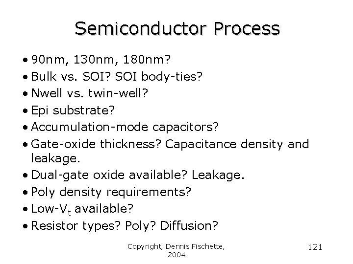
Semiconductor Process • 90 nm, 130 nm, 180 nm? • Bulk vs. SOI? SOI body-ties? • Nwell vs. twin-well? • Epi substrate? • Accumulation-mode capacitors? • Gate-oxide thickness? Capacitance density and leakage. • Dual-gate oxide available? Leakage. • Poly density requirements? • Low-Vt available? • Resistor types? Poly? Diffusion? Copyright, Dennis Fischette, 2004 121

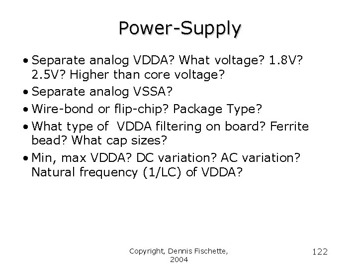
Power-Supply • Separate analog VDDA? What voltage? 1. 8 V? 2. 5 V? Higher than core voltage? • Separate analog VSSA? • Wire-bond or flip-chip? Package Type? • What type of VDDA filtering on board? Ferrite bead? What cap sizes? • Min, max VDDA? DC variation? AC variation? Natural frequency (1/LC) of VDDA? Copyright, Dennis Fischette, 2004 122

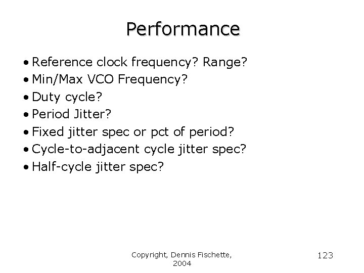
Performance • Reference clock frequency? Range? • Min/Max VCO Frequency? • Duty cycle? • Period Jitter? • Fixed jitter spec or pct of period? • Cycle-to-adjacent cycle jitter spec? • Half-cycle jitter spec? Copyright, Dennis Fischette, 2004 123

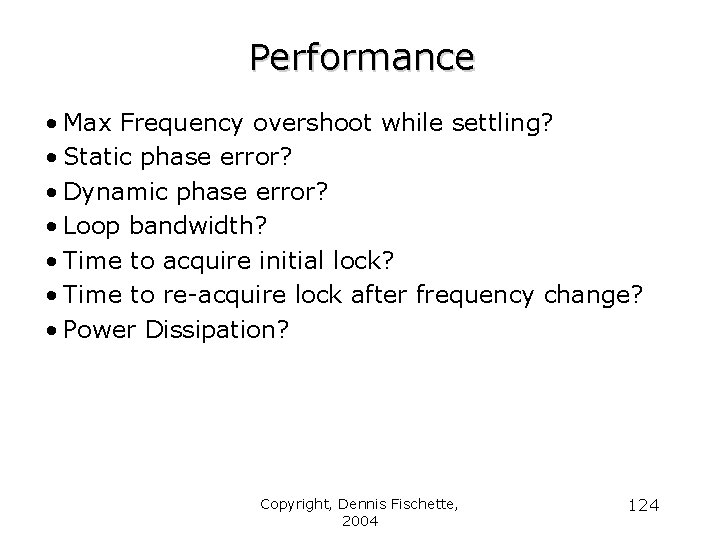
Performance • Max Frequency overshoot while settling? • Static phase error? • Dynamic phase error? • Loop bandwidth? • Time to acquire initial lock? • Time to re-acquire lock after frequency change? • Power Dissipation? Copyright, Dennis Fischette, 2004 124

Logic Interface • Reset available? • Power. OK available? • VCO/CP/R range settings allowed? • Clock glitching allowed when switching VCO frequency ranges? • Level-shift and buffer PLL inputs/outputs? • Different power domains? Copyright, Dennis Fischette, 2004 125

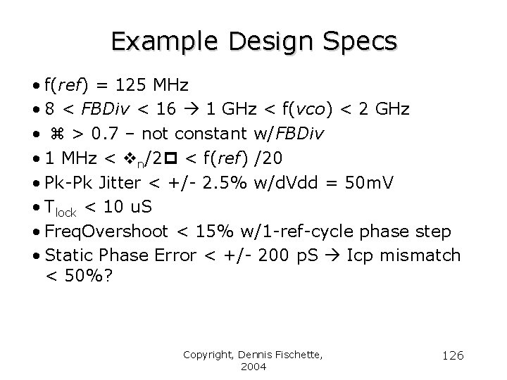
Example Design Specs • f(ref) = 125 MHz • 8 < FBDiv < 16 1 GHz < f(vco) < 2 GHz • > 0. 7 – not constant w/FBDiv • 1 MHz < n/2 < f(ref) /20 • Pk-Pk Jitter < +/- 2. 5% w/d. Vdd = 50 m. V • Tlock < 10 u. S • Freq. Overshoot < 15% w/1 -ref-cycle phase step • Static Phase Error < +/- 200 p. S Icp mismatch < 50%? Copyright, Dennis Fischette, 2004 126

References Copyright, Dennis Fischette, 2004 127
![Paper References 1 B Razavi Monolithic PhaseLocked Loops and ClockRecovery Circuits IEEE Press 1996 Paper References [1] B. Razavi, Monolithic Phase-Locked Loops and Clock-Recovery Circuits, IEEE Press, 1996.](https://slidetodoc.com/presentation_image/49fd03bf46a598ba555ccafd48606513/image-128.jpg)
Paper References [1] B. Razavi, Monolithic Phase-Locked Loops and Clock-Recovery Circuits, IEEE Press, 1996. – collection of IEEE PLL papers. [2] I. Young et al. , “A PLL clock generator with 5 to 110 MHz of lock range for microprocessors, ” IEEE J. Solid-State Circuits, vol. 27, no. 11, pp. 15991607, Nov. 1992. [3] J. Maneatis, “Low-Jitter Process-Independent DLL and PLL Based on Self. Biased Techniques”, IEEE J. Solid-State Circuits, vol. 31, no. 11, pp. 17231732. Nov. 1996. [4] J. Maneatis, “Self-Biased, High-Bandwidth, Low-Jitter 1 -to-4096 Multiplier Clock Generator PLL”, IEEE J. Solid-State Circuits, vol. 38, no. 11, pp. 17951803. Nov. 2003. [5] F. Gardner, “Charge-pump phase-lock loops, ” IEEE Trans. Commun. , vol COM-28, no. 11, pp 1849 -1858, Nov. 1980. [6] V. von Kaenel, “A 32 - MHz, 1. 5 m. W @ 1. 35 V CMOS PLL for Microprocessor Clock Generation”, IEEE J. Solid-State Circuits, vol. 31, no. 11, pp. 17151722. Nov. 1996. Copyright, Dennis Fischette, 2004 128
![Paper References cont 7 I Young A 0 35 um CMOS 3 880 Paper References (cont. ) [7] I. Young, “A 0. 35 um CMOS 3 -880](https://slidetodoc.com/presentation_image/49fd03bf46a598ba555ccafd48606513/image-129.jpg)
Paper References (cont. ) [7] I. Young, “A 0. 35 um CMOS 3 -880 MHz PLL N/2 Clock Multiplier and Distribution Network with Low Jitter for Microprocessors”, ISSCC 1997 Digest of Tech. Papers, session 20. 1, pp. 330 -331. [8] J. Ingino et al, “A 4 -GHz Clock System for a High-Performance System-on -a-Chip Design”, IEEE J. Solid-State Circuits, vol. 36, no. 11, pp. 1693 -1698. Nov. 2001. [9] A. Maxim, et al. , “A Low-Jitter 125 -1250 MHz Process-Independent CMOS PLL Based on a Sample-Reset Loop Filter”, 2001 ISSCC Digest Of Tech. Papers, pp. 394 -395. [10] N. Kurd, et al. , “A Replica-Biased 50% Duty Cycle PLL Architecture with 1 X VCO”, 2003 ISSCC Digest of Tech. Papers, session 24. 3, pp. 426 -427. [11] K. Wong, et al. , ”Cascaded PLL Design fpr a 90 nm CMOS High Performance Microprocessor”, 2003 ISSCC Digest of Tech. Papers, session 24. 3, pp. 422 -423. [12] M. Mansuri, et al. , “A Low-Power Adaptive-Bandwidth PLL and Clock Buffer With Supply-Noise Compensation”, IEEE J. Solid-State Circuits, vol. 38, no. 11, pp. 1804 -1812. Nov. 2003. Copyright, Dennis Fischette, 2004 129
![Paper References cont 7 A Maxim A 160 2550 MHz CMOS Active Clock Paper References (cont. ) [7] A. Maxim, “A 160 -2550 MHz CMOS Active Clock](https://slidetodoc.com/presentation_image/49fd03bf46a598ba555ccafd48606513/image-130.jpg)
Paper References (cont. ) [7] A. Maxim, “A 160 -2550 MHz CMOS Active Clock Deskewing PLL Using Analog Phase Interpolation”, ISSCC 2004 Digest of Tech. Papers, session 19. 3, pp. 346 -347. [8] Jerry Lin et al, “A PVT Tolerant 0. 18 MHz to 660 MHz Self-Calibrated Digital PLL in 90 nm CMOS Process”, ISSCC 2004 Digest of Tech. Papers, session 26. 10, pp. 488 -489. Copyright, Dennis Fischette, 2004 130
![Monograph References 1 B Razavi Design of Analog CMOS Integrated Circuits Mc GrawHill 2001 Monograph References [1] B. Razavi, Design of Analog CMOS Integrated Circuits, Mc. Graw-Hill, 2001.](https://slidetodoc.com/presentation_image/49fd03bf46a598ba555ccafd48606513/image-131.jpg)
Monograph References [1] B. Razavi, Design of Analog CMOS Integrated Circuits, Mc. Graw-Hill, 2001. [2] R. Best, Phase-Locked Loops, Mc. Graw-Hill, 1993. [3] R. Dorf, Modern Control Theory, 4 th Edition, Addison-Wesley, 1986. [4] P. Gray & R. Meyer, Analysis and Design of Analog Integrated Circuits, 3 rd Edition, J. Wiley & Sons, 1993. [5] K. Bernstein & N. Rohner, SOI Circuit Design Concepts, Kluwer Academic Publishers, 2000. [6] A. Hajimiri & T. Lee, The Design of Low Noise Oscillators, Kluwer Academic Publishers, 1999 [7] T. Lee, The Design of CMOS Radio-Frequency Integrated Circuits, Cambridge University Press, 1998. [8] F. Gardner, Phaselock Techniques, 2 nd Edition, New York, Wiley & Sons, 1979 Copyright, Dennis Fischette, 2004 131