ECE 448 Lab 3 Part 1 FPGA Design

ECE 448 Lab 3 – Part 1 FPGA Design Flow Based on Xilinx Vivado and Vivado Simulator. Using Seven-Segment Displays, Buttons, and Switches.

Agenda for today Part 1: Testing of FPGA boards Part 2: Seven Segment Displays Part 3: User Constraints File Part 4: Buttons and Switches Part 5: Introduction to FPGA Design Flow based on Xilinx Vivado and Vivado Simulator Part 6: Introduction to Lab 3 Part 7: Class Exercise Part 8: Demo Lab Assignment 2

Part 1 Testing of FPGA Boards

Part 2 Seven Segment Displays

Seven Segment Displays

4 -Digit Seven Segment Display

Patterns for Decimal Digits

Patterns for Hexadecimal Digits

Connection to FPGA Pins

Multiplexing Digits

Time-Multiplexed Seven Segment Display
 Counter UP Cou clk nter Cou UP rst nter UP")
SSD_DRIVER seg(6. . 0) Counter UP Cou clk nter Cou UP rst nter UP COUNTER UP Counter UP q(k-1. . k-2) Counter UP OC OC – One’s Complement an

Size of the counter 1 ms ≤ 2 k * TCLK ≤ 16 ms f. CLK = 100 MHz k = ?
")
Part 3 Xilinx Design Constraints (XDC)
 • File contains various constraints for Xilinx – Clock Period")
Xilinx Design Constraints (XDC) • File contains various constraints for Xilinx – Clock Period – Circuit Locations – Pin Locations • Every pin in the top-level unit needs to have a pin in the XDC

Basys 3 General I/O Devices

BASYS 3 XDC – Seven Segment Display #7 segment display set_property PACKAGE_PIN W 7 [get_ports {seg[0]}] set_property IOSTANDARD LVCMOS 33 [get_ports {seg[0]}] set_property PACKAGE_PIN W 6 [get_ports {seg[1]}] set_property IOSTANDARD LVCMOS 33 [get_ports {seg[1]}] set_property PACKAGE_PIN U 8 [get_ports {seg[2]}] set_property IOSTANDARD LVCMOS 33 [get_ports {seg[2]}] set_property PACKAGE_PIN V 8 [get_ports {seg[3]}] set_property IOSTANDARD LVCMOS 33 [get_ports {seg[3]}] set_property PACKAGE_PIN U 5 [get_ports {seg[4]}] set_property IOSTANDARD LVCMOS 33 [get_ports {seg[4]}] set_property PACKAGE_PIN V 5 [get_ports {seg[5]}] set_property IOSTANDARD LVCMOS 33 [get_ports {seg[5]}] set_property PACKAGE_PIN U 7 [get_ports {seg[6]}] set_property IOSTANDARD LVCMOS 33 [get_ports {seg[6]}]
![BASYS 3 XDC – Seven Segment Display #set_property PACKAGE_PIN V 7 [get_ports dp] #set_property](http://slidetodoc.com/presentation_image_h/1885d07934bdc4c4bdb21735b9859025/image-18.jpg "BASYS 3 XDC – Seven Segment Display #set_property PACKAGE_PIN V 7 [get_ports dp] #set_property")
BASYS 3 XDC – Seven Segment Display #set_property PACKAGE_PIN V 7 [get_ports dp] #set_property IOSTANDARD LVCMOS 33 [get_ports dp] set_property PACKAGE_PIN U 2 [get_ports {an[0]}] set_property IOSTANDARD LVCMOS 33 [get_ports {an[0]}] set_property PACKAGE_PIN U 4 [get_ports {an[1]}] set_property IOSTANDARD LVCMOS 33 [get_ports {an[1]}] set_property PACKAGE_PIN V 4 [get_ports {an[2]}] set_property IOSTANDARD LVCMOS 33 [get_ports {an[2]}] set_property PACKAGE_PIN W 4 [get_ports {an[3]}] set_property IOSTANDARD LVCMOS 33 [get_ports {an[3]}]
![BASYS 3 XDC - LEDs # LEDs set_property PACKAGE_PIN U 16 [get_ports {led[0]}] set_property](http://slidetodoc.com/presentation_image_h/1885d07934bdc4c4bdb21735b9859025/image-19.jpg "BASYS 3 XDC - LEDs # LEDs set_property PACKAGE_PIN U 16 [get_ports {led[0]}] set_property")
BASYS 3 XDC - LEDs # LEDs set_property PACKAGE_PIN U 16 [get_ports {led[0]}] set_property IOSTANDARD LVCMOS 33 [get_ports {led[0]}] set_property PACKAGE_PIN E 19 [get_ports {led[1]}] set_property IOSTANDARD LVCMOS 33 [get_ports {led[1]}] set_property PACKAGE_PIN U 19 [get_ports {led[2]}] set_property IOSTANDARD LVCMOS 33 [get_ports {led[2]}] set_property PACKAGE_PIN V 19 [get_ports {led[3]}] set_property IOSTANDARD LVCMOS 33 [get_ports {led[3]}] set_property PACKAGE_PIN W 18 [get_ports {led[4]}] set_property IOSTANDARD LVCMOS 33 [get_ports {led[4]}] set_property PACKAGE_PIN U 15 [get_ports {led[5]}] set_property IOSTANDARD LVCMOS 33 [get_ports {led[5]}]
![BASYS 3 XDC - LEDs set_property PACKAGE_PIN U 14 [get_ports {led[6]}] set_property IOSTANDARD LVCMOS](http://slidetodoc.com/presentation_image_h/1885d07934bdc4c4bdb21735b9859025/image-20.jpg "BASYS 3 XDC - LEDs set_property PACKAGE_PIN U 14 [get_ports {led[6]}] set_property IOSTANDARD LVCMOS")
BASYS 3 XDC - LEDs set_property PACKAGE_PIN U 14 [get_ports {led[6]}] set_property IOSTANDARD LVCMOS 33 [get_ports {led[6]}] set_property PACKAGE_PIN V 14 [get_ports {led[7]}] set_property IOSTANDARD LVCMOS 33 [get_ports {led[7]}] set_property PACKAGE_PIN V 13 [get_ports {led[8]}] set_property IOSTANDARD LVCMOS 33 [get_ports {led[8]}] set_property PACKAGE_PIN V 3 [get_ports {led[9]}] set_property IOSTANDARD LVCMOS 33 [get_ports {led[9]}] set_property PACKAGE_PIN W 3 [get_ports {led[10]}] set_property IOSTANDARD LVCMOS 33 [get_ports {led[10]}] set_property PACKAGE_PIN U 3 [get_ports {led[11]}] set_property IOSTANDARD LVCMOS 33 [get_ports {led[11]}] set_property PACKAGE_PIN P 3 [get_ports {led[12]}] set_property IOSTANDARD LVCMOS 33 [get_ports {led[12]}]
![BASYS 3 XDC - LEDs set_property PACKAGE_PIN N 3 [get_ports {led[13]}] set_property IOSTANDARD LVCMOS](http://slidetodoc.com/presentation_image_h/1885d07934bdc4c4bdb21735b9859025/image-21.jpg "BASYS 3 XDC - LEDs set_property PACKAGE_PIN N 3 [get_ports {led[13]}] set_property IOSTANDARD LVCMOS")
BASYS 3 XDC - LEDs set_property PACKAGE_PIN N 3 [get_ports {led[13]}] set_property IOSTANDARD LVCMOS 33 [get_ports {led[13]}] set_property PACKAGE_PIN P 1 [get_ports {led[14]}] set_property IOSTANDARD LVCMOS 33 [get_ports {led[14]}] set_property PACKAGE_PIN L 1 [get_ports {led[15]}] set_property IOSTANDARD LVCMOS 33 [get_ports {led[15]}]
![BASYS 3 XDC CLOCK # Clock signal set_property PACKAGE_PIN W 5 [get_ports clk] set_property](http://slidetodoc.com/presentation_image_h/1885d07934bdc4c4bdb21735b9859025/image-22.jpg "BASYS 3 XDC CLOCK # Clock signal set_property PACKAGE_PIN W 5 [get_ports clk] set_property")
BASYS 3 XDC CLOCK # Clock signal set_property PACKAGE_PIN W 5 [get_ports clk] set_property IOSTANDARD LVCMOS 33 [get_ports clk] create_clock -add -name sys_clk_pin -period 10. 00 -waveform {0 5} [get_ports clk]

Part 4 Switches and Buttons
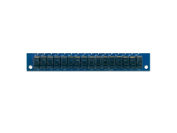

Basys 3 Slide Switches
![BASYS 3 XDC – Switches # Switches set_property PACKAGE_PIN V 17 [get_ports {sw[0]}] set_property](http://slidetodoc.com/presentation_image_h/1885d07934bdc4c4bdb21735b9859025/image-26.jpg "BASYS 3 XDC – Switches # Switches set_property PACKAGE_PIN V 17 [get_ports {sw[0]}] set_property")
BASYS 3 XDC – Switches # Switches set_property PACKAGE_PIN V 17 [get_ports {sw[0]}] set_property IOSTANDARD LVCMOS 33 [get_ports{sw[0]}] set_property PACKAGE_PIN V 16 [get_ports {sw[1]}] set_property IOSTANDARD LVCMOS 33 [get_ports {sw[1]}] set_property PACKAGE_PIN W 16 [get_ports {sw[2]}] set_property IOSTANDARD LVCMOS 33 [get_ports {sw[2]}] set_property PACKAGE_PIN W 17 [get_ports {sw[3]}] set_property IOSTANDARD LVCMOS 33 [get_ports {sw[3]}] set_property PACKAGE_PIN W 15 [get_ports {sw[4]}] set_property IOSTANDARD LVCMOS 33 [get_ports {sw[4]}] set_property PACKAGE_PIN V 15 [get_ports {sw[5]}] set_property IOSTANDARD LVCMOS 33 [get_ports {sw[5]}] set_property PACKAGE_PIN W 14 [get_ports {sw[6]}] set_property IOSTANDARD LVCMOS 33 [get_ports {sw[6]}] set_property PACKAGE_PIN W 13 [get_ports {sw[7]}] set_property IOSTANDARD LVCMOS 33 [get_ports {sw[7]}]
![BASYS 3 XDC – Switches (2) set_property PACKAGE_PIN V 2 [get_ports {sw[8]}] set_property IOSTANDARD](http://slidetodoc.com/presentation_image_h/1885d07934bdc4c4bdb21735b9859025/image-27.jpg "BASYS 3 XDC – Switches (2) set_property PACKAGE_PIN V 2 [get_ports {sw[8]}] set_property IOSTANDARD")
BASYS 3 XDC – Switches (2) set_property PACKAGE_PIN V 2 [get_ports {sw[8]}] set_property IOSTANDARD LVCMOS 33 [get_ports {sw[8]}] set_property PACKAGE_PIN T 3 [get_ports {sw[9]}] set_property IOSTANDARD LVCMOS 33 [get_ports {sw[9]}] set_property PACKAGE_PIN T 2 [get_ports {sw[10]}] set_property IOSTANDARD LVCMOS 33 [get_ports {sw[10]}] set_property PACKAGE_PIN R 3 [get_ports {sw[11]}] set_property IOSTANDARD LVCMOS 33 [get_ports {sw[11]}] set_property PACKAGE_PIN W 2 [get_ports {sw[12]}] set_property IOSTANDARD LVCMOS 33 [get_ports {sw[12]}] set_property PACKAGE_PIN U 1 [get_ports {sw[13]}] set_property IOSTANDARD LVCMOS 33 [get_ports {sw[13]}] set_property PACKAGE_PIN T 1 [get_ports {sw[14]}] set_property IOSTANDARD LVCMOS 33 [get_ports {sw[14]}] set_property PACKAGE_PIN R 2 [get_ports {sw[15]}] set_property IOSTANDARD LVCMOS 33 [get_ports {sw[15]}]

Buttons

Connection of Buttons to FPGA Pins

Debouncing Buttons key bounce, t. BOUNCE Bouncing period typically smaller than 10 ms
 RED – Rising Edge Detector")
Using DEBOUNCE_RED to Generate Short Pulses (1) RED – Rising Edge Detector
")
Using DEBOUNCE_RED to Generate Short Pulses (2)

Debouncer reset input clk output Debouncer

Debouncer

k and DD Generics k - width of the counter used to measure the debouncing period DD - debouncing period in clock cycles Values of generics given on the next slide assume that the clock frequency = 100 MHz and thus clock period = 10 ns.
: DD = 100")
k and DD Generics Option 1 (value used for simulation only): DD = 100 assuming bouncing period < 1 μs = 1000 ns condition: DD*10 ns = 1000 ns => DD = 100 k=7 because 2^7 > 100 Option 2 (values used for synthesis, implementation, and experimental testing): DD = 1000000 assuming bouncing period = 10 ms condition: DD*10 ns = 10 ms => DD = 1, 000 k=20 because 2^20 > 1, 000

Rising Edge Detector - RED Rising Edge Detector • Turn a step function into an impulse • Allows a step to run a circuit for only one clock cycle

Rising Edge Detector reset rising edge detector input q output clk input q output

Connection of Buttons to FPGA Pins
![BASYS 3 XDC – Buttons #Buttons set_property PACKAGE_PIN U 18 [get_ports btn. C] set_property](http://slidetodoc.com/presentation_image_h/1885d07934bdc4c4bdb21735b9859025/image-40.jpg "BASYS 3 XDC – Buttons #Buttons set_property PACKAGE_PIN U 18 [get_ports btn. C] set_property")
BASYS 3 XDC – Buttons #Buttons set_property PACKAGE_PIN U 18 [get_ports btn. C] set_property IOSTANDARD LVCMOS 33 [get_ports btn. C] set_property PACKAGE_PIN T 18 [get_ports btn. U] set_property IOSTANDARD LVCMOS 33 [get_ports btn. U] set_property PACKAGE_PIN W 19 [get_ports btn. L] set_property IOSTANDARD LVCMOS 33 [get_ports btn. L] set_property PACKAGE_PIN T 17 [get_ports btn. R] set_property IOSTANDARD LVCMOS 33 [get_ports btn. R] set_property PACKAGE_PIN U 17 [get_ports btn. D] set_property IOSTANDARD LVCMOS 33 [get_ports btn. D]

Part 5 Hands-on Session on FPGA Design Flow based on Xilinx Vivado and Vivado Simulator

Part 6 Introduction to Lab 3 Automated Teller Machine ATM
 Cash Withdrawal (COUT) Deposit")
ATM Services 1. 2. 3. 4. 5. Balance Inquiry (BAL) Cash Withdrawal (COUT) Deposit Cash (CIN) Deposit a Check (CHEC) Change PIN (CPIN)

Step 1: Entering a PIN Number Default Enter PIN using switches Move to STEP 2
 BTNR (RIGHT) BTNL LEFT BTNS (Enter)")
Step 2: Choosing an Option Default BTNU (UP) BTNR (RIGHT) BTNL LEFT BTNS (Enter) BTND DOWN

Balance Inquiry • If “Balance Inquiry” chosen first time • For Every other “Balance Inquiry”, display the available balance on 7 segment display • To go to Step 2 BTNS (Enter)

Cash Withdrawal $10 $50 $100 $20 Amount entered using Buttons

Cash Withdrawal • If amount entered is not a multiple of $20 or greater than $500, display • For Insufficient funds, Display • If amount entered is a valid amount, it should blink for 5 seconds on the 7 -segment display, and the remaining amount is displayed afterwards.

Cash Deposit $10 $50 $100 $20 Amount entered using Buttons

Cash Deposit • Total deposit amount is displayed on the seven segment display, starting from 0. • Available Balance = Previous Balance + Deposit Amount • If available balance is greater than the allowed balance ($1500), display and reset the deposit amount to 0. • If amount entered is a valid amount, it should blink for 5 seconds on the 7 -segment display, and the Available Balance is displayed afterwards.

Check Deposit • Check value specified in BCD notation entered using Switches. • Available Balance = Previous Balance + Deposit Amount • If available balance is greater than the allowed balance ($1500), display and reset the deposit amount to 0. • If amount entered is a valid amount, it should blink for 5 seconds on the 7 -segment display, and the Available Balance is displayed afterwards.

Change PIN • New 8 -bit PIN entered using Switches • If new PIN matches the old PIN, display Otherwise update the new PIN

Part 7 Lab Exercise

16 -bit Binary Up-Down Counter
 Counter UP Cou clk nter Cou UP rst nter UP")
SSD_DRIVER SEG(6. . 0) Counter UP Cou clk nter Cou UP rst nter UP COUNTER UP Counter UP q(k-1. . k-2) Counter UP OC OC – One’s Complement AN

Part 8 Lab Assignment 2: Demo
- Slides: 56