Design Methodology for HighDensity FPGA Design Selecting an




- Slides: 77
Design Methodology for High-Density FPGA Design Selecting an Architecture High-Density Software Methodology Implementation and Integration of Cores 1 Design Methodology
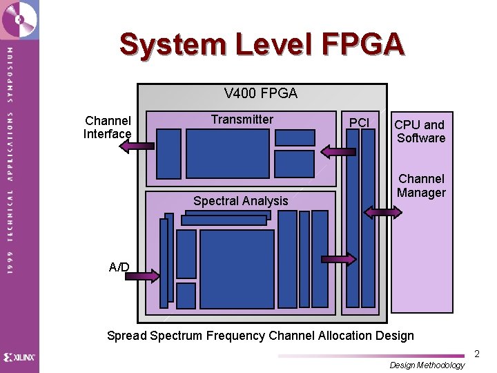
System Level FPGA V 400 FPGA Channel Interface Transmitter Spectral Analysis PCI CPU and Software Channel Manager A/D Spread Spectrum Frequency Channel Allocation Design 2 Design Methodology
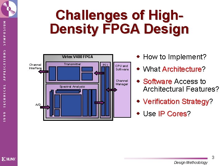
Challenges of High. Density FPGA Design w How to Implement? Virtex V 400 FPGA Channel Interface Transmitter Spectral Analysis A/D PCI CPU and Software Channel Manager w What Architecture? Architecture w Software Access to Architectural Features? w Verification Strategy? Strategy w Use IP Cores? Cores 3 Design Methodology
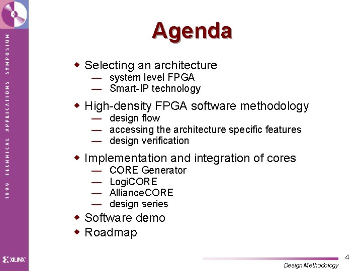
Agenda w Selecting an architecture — system level FPGA — Smart-IP technology w High-density FPGA software methodology — design flow — accessing the architecture specific features — design verification w Implementation and integration of cores — — CORE Generator Logi. CORE Alliance. CORE design series w Software demo w Roadmap 4 Design Methodology
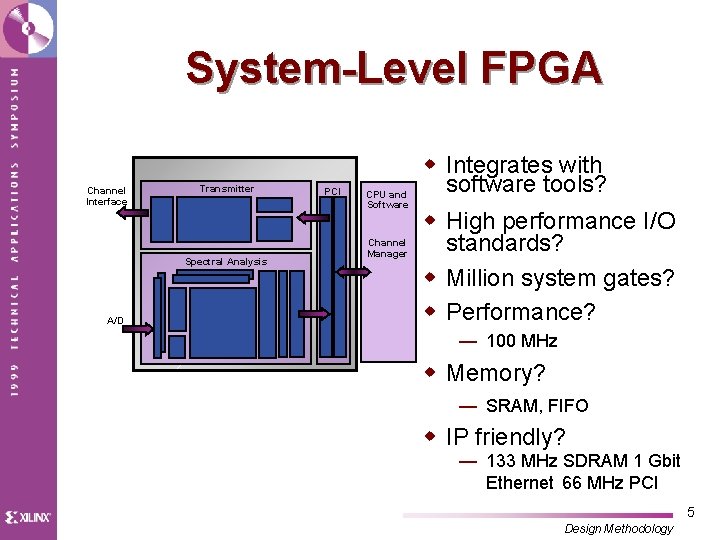
System-Level FPGA Channel Interface Transmitter Spectral Analysis A/D PCI CPU and Software Channel Manager w Integrates with software tools? w High performance I/O standards? w Million system gates? w Performance? — 100 MHz w Memory? — SRAM, FIFO w IP friendly? — 133 MHz SDRAM 1 Gbit Ethernet 66 MHz PCI 5 Design Methodology
Xilinx Smart-IP Technology w Xilinx Smart-IP Technology — architectures tailored to cores — intelligent software implementation — flexible core technology w Delivers: — high predictability — high performance — high flexibility Only available from Xilinx 6 Design Methodology
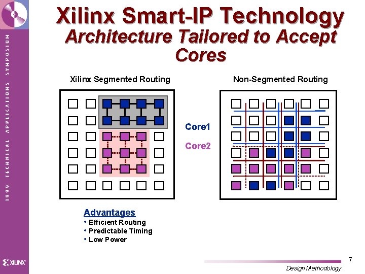
Xilinx Smart-IP Technology Architecture Tailored to Accept Cores Xilinx Segmented Routing Non-Segmented Routing Core 1 Core 2 Advantages • Efficient Routing • Predictable Timing • Low Power 7 Design Methodology
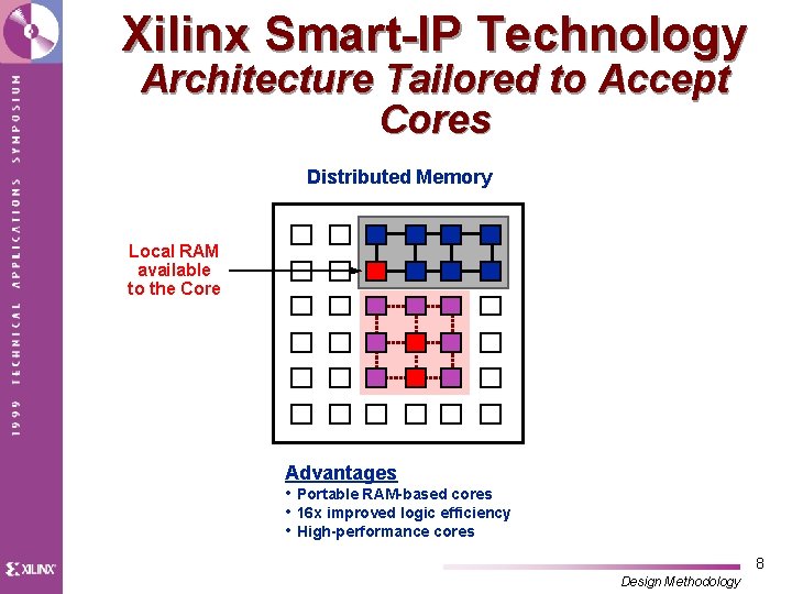
Xilinx Smart-IP Technology Architecture Tailored to Accept Cores Distributed Memory Local RAM available to the Core Advantages • Portable RAM-based cores • 16 x improved logic efficiency • High-performance cores 8 Design Methodology
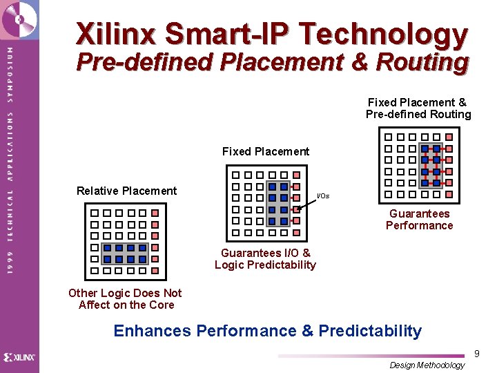
Xilinx Smart-IP Technology Pre-defined Placement & Routing Fixed Placement & Pre-defined Routing Fixed Placement Relative Placement I/Os Guarantees Performance Guarantees I/O & Logic Predictability Other Logic Does Not Affect on the Core Enhances Performance & Predictability 9 Design Methodology
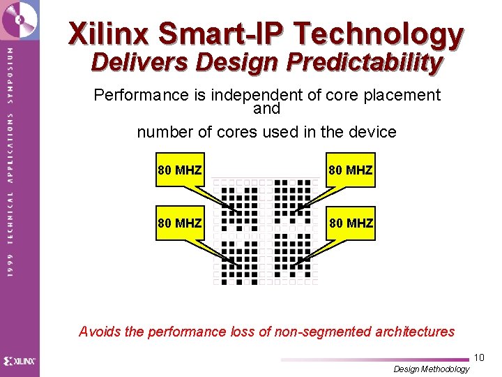
Xilinx Smart-IP Technology Delivers Design Predictability Performance is independent of core placement and number of cores used in the device 80 MHZ Avoids the performance loss of non-segmented architectures 10 Design Methodology
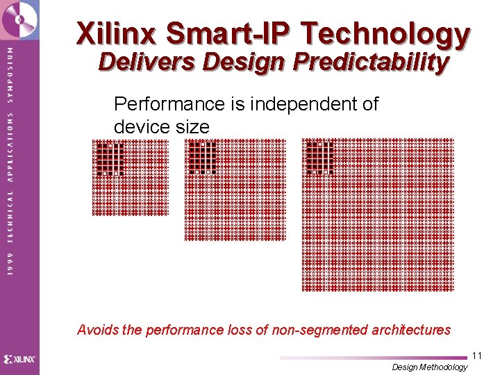
Xilinx Smart-IP Technology Delivers Design Predictability Performance is independent of device size Avoids the performance loss of non-segmented architectures 11 Design Methodology
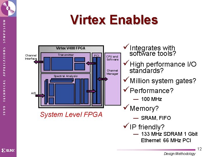
Virtex Enables üIntegrates with Virtex V 400 FPGA Channel Interface Transmitter PCI Spectral Analysis A/D CPU and Software Channel Manager software tools? üHigh performance I/O standards? üMillion system gates? üPerformance? — 100 MHz System Level FPGA üMemory? — SRAM, FIFO üIP friendly? — 133 MHz SDRAM 1 Gbit Ethernet 66 MHz PCI 12 Design Methodology
Agenda üSelecting an architecture — system level FPGA — Smart-IP technology w High-density FPGA software methodology — design flow — accessing the architecture specific features — design verification w Implementation and integration of cores — — CORE Generator Logi. CORE Alliance. CORE design series w Software demo w Roadmap 13 Design Methodology
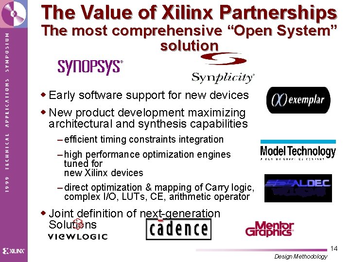
The Value of Xilinx Partnerships The most comprehensive “Open System” solution w Early software support for new devices w New product development maximizing architectural and synthesis capabilities – efficient timing constraints integration – high performance optimization engines tuned for new Xilinx devices – direct optimization & mapping of Carry logic, complex I/O, LUTs, CE, arithmetic operator w Joint definition of next-generation Solutions 14 Design Methodology
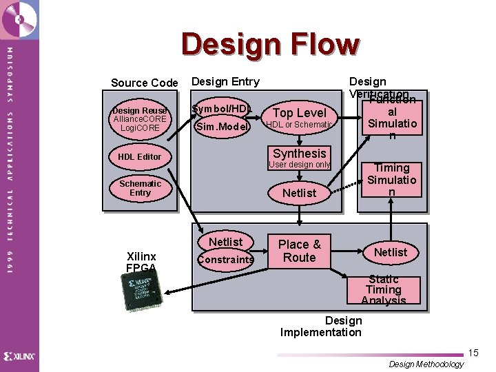
Design Flow Source Code Design Entry Design Reuse Alliance. CORE Logi. CORE Symbol/HDL Sim. Model HDL or Schematic Synthesis HDL Editor User design only Schematic Entry Timing Simulatio n Netlist Xilinx FPGA Top Level Design Verification Function al Simulatio n Constraints Place & Route Netlist Static Timing Analysis Design Implementation 15 Design Methodology
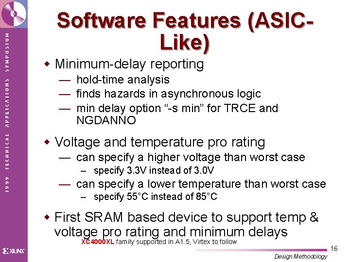
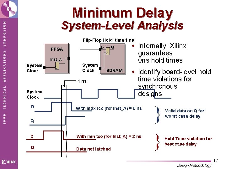
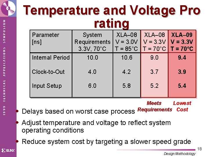
Software Features (ASICLike) w Minimum-delay reporting — hold-time analysis — finds hazards in asynchronous logic — min delay option “-s min” for TRCE and NGDANNO w Voltage and temperature pro rating — can specify a higher voltage than worst case – specify 3. 3 V instead of 3. 0 V — can specify a lower temperature than worst case – specify 55°C instead of 85°C w First SRAM based device to support temp & voltage pro rating and minimum delays XC 4000 XL family supported in A 1. 5, Virtex to follow 16 Design Methodology
Minimum Delay System-Level Analysis Flip-Flop Hold time 1 ns Q D FPGA Inst_A System Clock SDRAM 1 ns System Clock D w Internally, Xilinx guarantees 0 ns hold times w Identify board-level hold time violations for synchronous designs With max tco (for Inst_A) = 5 ns Q D With min tco (for Inst_A) = 2 ns Q Data not latched } } Valid data on Q for worst case delay Hold Time violation for best case delay 17 Design Methodology
Temperature and Voltage Pro rating Parameter [ns] System XLA– 08 XLA– 09 Requirements V = 3. 0 V V = 3. 3 V, 70°C T = 85°C T = 70°C Internal Period 9. 4 9. 0 10. 6 Clock-to-Out 4. 0 4. 2 3. 7 3. 9 Input Setup 6. 0 5. 8 5. 2 5. 4 w Delays based on worst case process Lowest Meets Requirements Cost w Adjust temperature and voltage to reflect system operating conditions w Reduce system cost by targeting a slower speed grade 18 Design Methodology
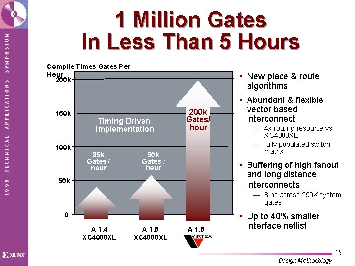
1 Million Gates In Less Than 5 Hours Compile Times Gates Per Hour 200 k 150 k 100 k w New place & route algorithms Timing Driven Implementation 35 k Gates / hour 200 k Gates/ hour 50 k Gates / hour w Abundant & flexible vector based interconnect — 4 x routing resource vs XC 4000 XL — fully populated switch matrix w Buffering of high fanout and long distance interconnects 50 k — 8 ns across 250 K system gates 0 A 1. 4 XC 4000 XL A 1. 5 w Up to 40% smaller interface netlist 19 Design Methodology
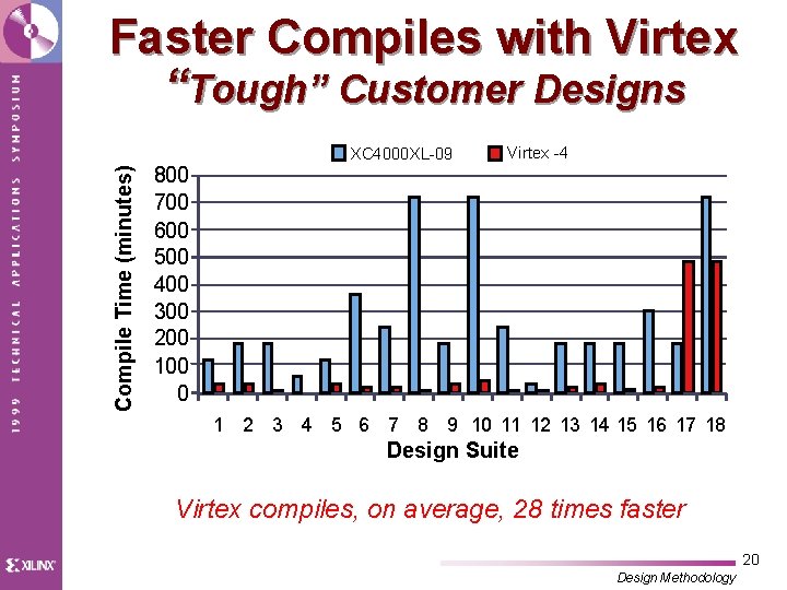
Compile Time (minutes) Faster Compiles with Virtex “Tough” Customer Designs 800 700 600 500 400 300 200 100 0 XC 4000 XL-09 Virtex -4 1 2 3 4 5 6 7 8 9 10 11 12 13 14 15 16 17 18 Design Suite Virtex compiles, on average, 28 times faster 20 Design Methodology
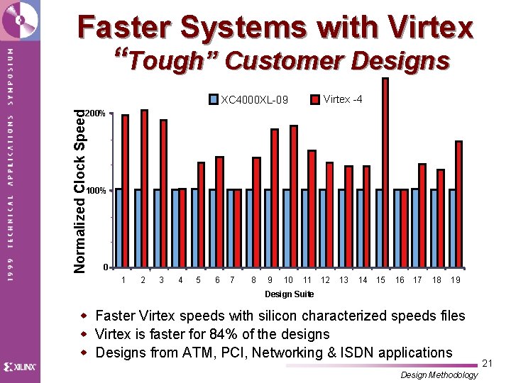
Faster Systems with Virtex “Tough” Customer Designs Virtex -4 XC 4000 XL-09 Normalized Clock Speed 200% 100% 0 1 2 3 4 5 6 7 8 9 10 11 12 13 14 15 16 17 18 19 Design Suite w Faster Virtex speeds with silicon characterized speeds files w Virtex is faster for 84% of the designs w Designs from ATM, PCI, Networking & ISDN applications Design Methodology 21
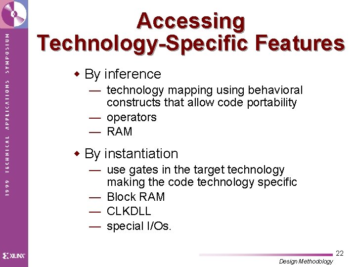
Accessing Technology-Specific Features w By inference — technology mapping using behavioral constructs that allow code portability — operators — RAM w By instantiation — use gates in the target technology making the code technology specific — Block RAM — CLKDLL — special I/Os. 22 Design Methodology
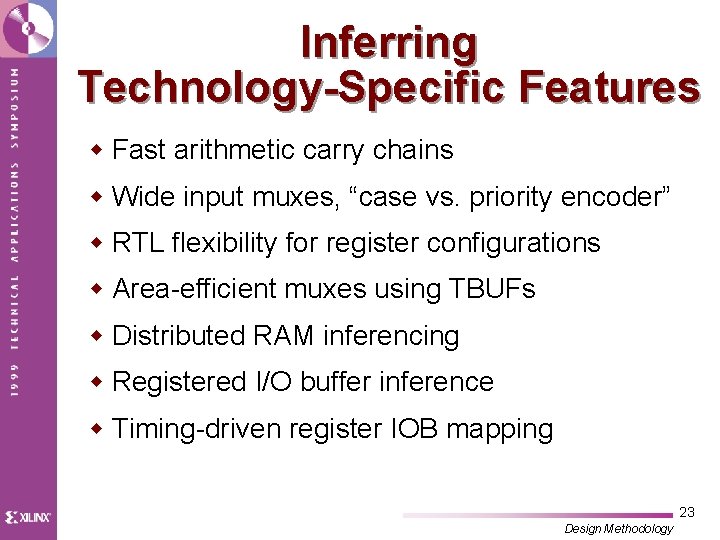
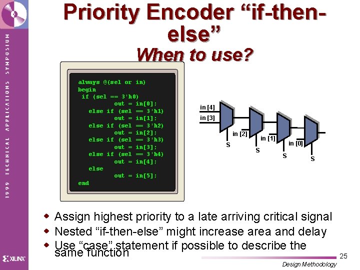
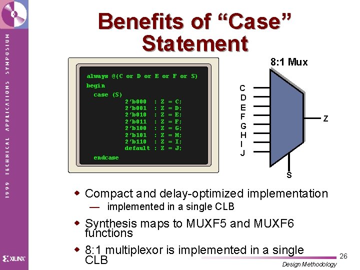
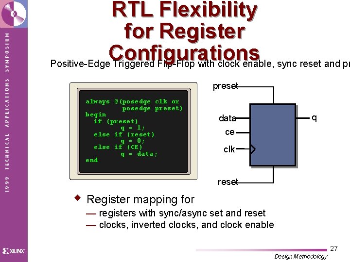
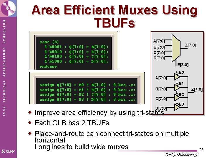
Inferring Technology-Specific Features w Fast arithmetic carry chains w Wide input muxes, “case vs. priority encoder” w RTL flexibility for register configurations w Area-efficient muxes using TBUFs w Distributed RAM inferencing w Registered I/O buffer inference w Timing-driven register IOB mapping 23 Design Methodology
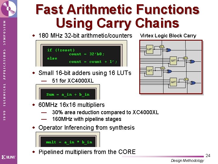
Fast Arithmetic Functions Using Carry Chains w 180 MHz 32 -bit arithmetic/counters Virtex Logic Block Carry 0 1 if (!reset) count = 32’b 0; else count = count + 1’; LUT w Small 16 -bit adders using 16 LUTs LUT 0 1 — 51 for XC 4000 XL 0 1 LUT Sum = a_in + b_in w 60 MHz 16 x 16 multipliers — 30% area reduction compared to XC 4000 XL — 160 MHz with pipeline stages w Operator Inferencing from synthesis mult = a_in * b_in w Pipelined multipliers from the CORE 24 Design Methodology
Priority Encoder “if-thenelse” When to use? always @(sel or in) begin if (sel == 3'h 0) out = in[0]; else if (sel == 3'h 1) out = in[1]; else if (sel == 3'h 2) out = in[2]; else if (sel == 3'h 3) out = in[3]; else if (sel == 3'h 4) out = in[4]; else out = in[5]; end in [4] in [3] in [2] S in [1] S in [0] S S w Assign highest priority to a late arriving critical signal w Nested “if-then-else” might increase area and delay w Use “case” statement if possible to describe the same function Design Methodology 25
Benefits of “Case” Statement 8: 1 Mux always @(C or D or E or F or S) begin case (S) 2’b 000 2’b 001 2’b 010 2’b 011 2’b 100 2’b 101 2’b 110 default : : : : Z Z Z Z = = = = C; D; E; F; G; H; I; J; endcase C D E F G H I J Z S w Compact and delay-optimized implementation — implemented in a single CLB w Synthesis maps to MUXF 5 and MUXF 6 functions w 8: 1 multiplexor is implemented in a single 26 CLB Design Methodology
RTL Flexibility for Register Configurations Positive-Edge Triggered Flip-Flop with clock enable, sync reset and pr preset always @(posedge clk or posedge preset) begin if (preset) q = 1; else if (reset) q = 0; else if (CE) q = data; end q data ce clk reset w Register mapping for — registers with sync/async set and reset — clocks, inverted clocks, and clock enable 27 Design Methodology
Area Efficient Muxes Using TBUFs case (E) 4’b 0001 4’b 0010 4’b 0100 4’b 1000 endcase : : Q[7: 0] = = A[7: 0] B[7: 0] C[7: 0] D[7: 0] A[7: 0]; B[7: 0]; C[7: 0]; D[7: 0]; Z[7: 0] E[3: 0] E 0 A[7: 0] assign Q[7: 0] = = E 0 E 1 E 2 E 3 ? ? A[7: 0] B[7: 0] C[7: 0] D[7: 0] : : 8'bzz. . z; E 1 B[7: 0] C[7: 0] D[7: 0] Z[7: 0] E 2 E 3 w Improve area efficiency by using tri-states w Each CLB has 2 TBUFs w Place-and-route can connect tri-states on multiple horizontal Longlines to build wide muxes Design Methodology 28
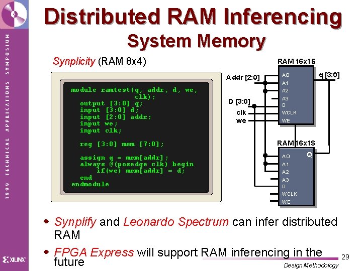
Distributed RAM Inferencing System Memory Synplicity (RAM 8 x 4) RAM 16 x 1 S Addr [2: 0] module ramtest(q, addr, d, we, clk); output [3: 0] q; input [3: 0] d; input [2: 0] addr; input we; input clk; reg [3: 0] mem [7: 0]; assign q = mem[addr]; always @(posedge clk) begin if(we) mem[addr] = d; endmodule q [3: 0] AO A 1 A 2 D [3: 0] clk we A 3 D WCLK WE RAM 16 x 1 S AO Q A 1 A 2 A 3 D WCLK WE w Synplify and Leonardo Spectrum can infer distributed RAM w FPGA Express will support RAM inferencing in the 29 future Design Methodology
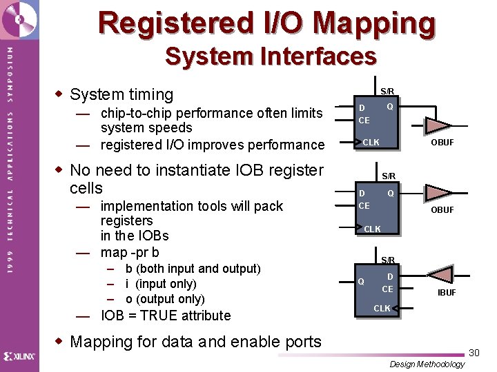
Registered I/O Mapping System Interfaces w System timing — chip-to-chip performance often limits system speeds — registered I/O improves performance w No need to instantiate IOB register cells — implementation tools will pack registers in the IOBs — map -pr b – b (both input and output) – i (input only) – o (output only) — IOB = TRUE attribute S/R Q D CE OBUF CLK S/R D CE Q OBUF CLK S/R Q D CE IBUF CLK w Mapping for data and enable ports 30 Design Methodology
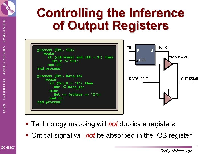
Controlling the Inference of Output Registers process (Tri, Clk) begin if (clk’event and clk =`1`) then Tri_R <= Tri; end if; end process; process (Tri, Data_in) begin if (Tri_R = ‘ 1’) then Out <= Data_in; else Out <= (others => ‘Z’); end if; end process; TRI D CLK Q TRI_R fanout = 24 DATA [23: 0] OUT [23: 0] w Technology mapping will not duplicate registers w Critical signal will not be absorbed in the IOB register 31 Design Methodology
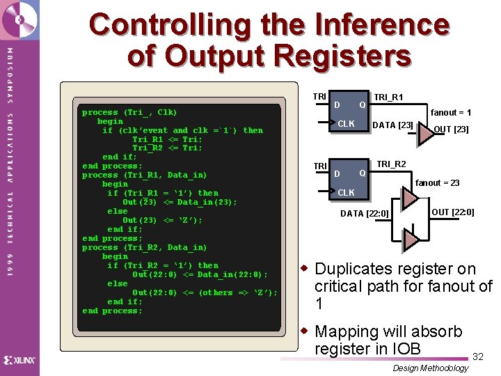
Controlling the Inference of Output Registers TRI process (Tri_, Clk) begin if (clk’event and clk =`1`) then Tri_R 1 <= Tri; Tri_R 2 <= Tri; end if; end process; process (Tri_R 1, Data_in) begin if (Tri_R 1 = ‘ 1’) then Out(23) <= Data_in(23); else Out(23) <= ‘Z’); end if; end process; process (Tri_R 2, Data_in) begin if (Tri_R 2 = ‘ 1’) then Out(22: 0) <= Data_in(22: 0); else Out(22: 0) <= (others => ‘Z’); end if; end process; D Q CLK TRI fanout = 1 DATA [23] Q D TRI_R 1 OUT [23] TRI_R 2 fanout = 23 CLK DATA [22: 0] OUT [22: 0] w Duplicates register on critical path for fanout of 1 w Mapping will absorb register in IOB Design Methodology 32
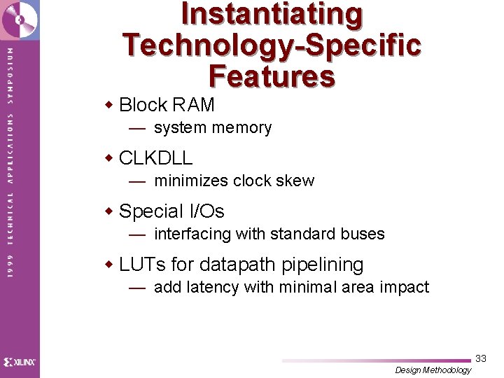
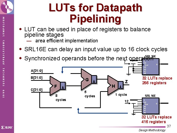
Instantiating Technology-Specific Features w Block RAM — system memory w CLKDLL — minimizes clock skew w Special I/Os — interfacing with standard buses w LUTs for datapath pipelining — add latency with minimal area impact 33 Design Methodology
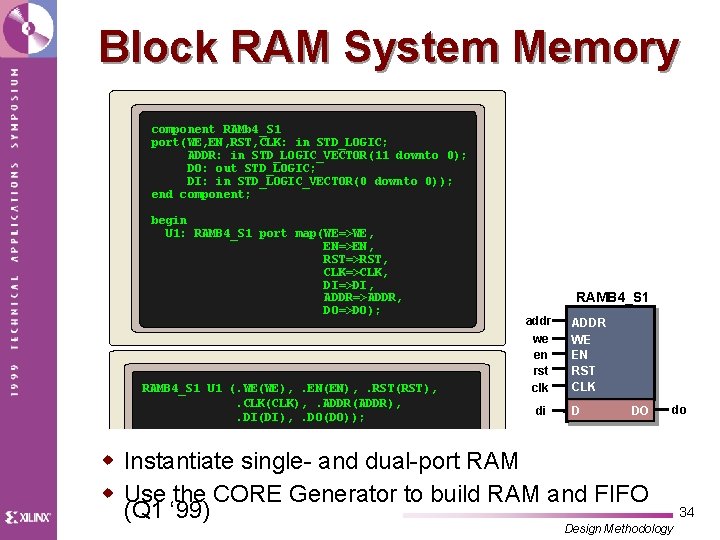
Block RAM System Memory component RAMb 4_S 1 port(WE, EN, RST, CLK: in STD_LOGIC; ADDR: in STD_LOGIC_VECTOR(11 downto 0); DO: out STD_LOGIC; DI: in STD_LOGIC_VECTOR(0 downto 0)); end component; begin U 1: RAMB 4_S 1 port map(WE=>WE, EN=>EN, RST=>RST, CLK=>CLK, DI=>DI, ADDR=>ADDR, DO=>DO); RAMB 4_S 1 U 1 (. WE(WE), . EN(EN), . RST(RST), . CLK(CLK), . ADDR(ADDR), . DI(DI), . DO(DO)); RAMB 4_S 1 addr we en rst clk di ADDR WE EN RST CLK D DO w Instantiate single- and dual-port RAM w Use the CORE Generator to build RAM and FIFO (Q 1 ‘ 99) do Design Methodology 34
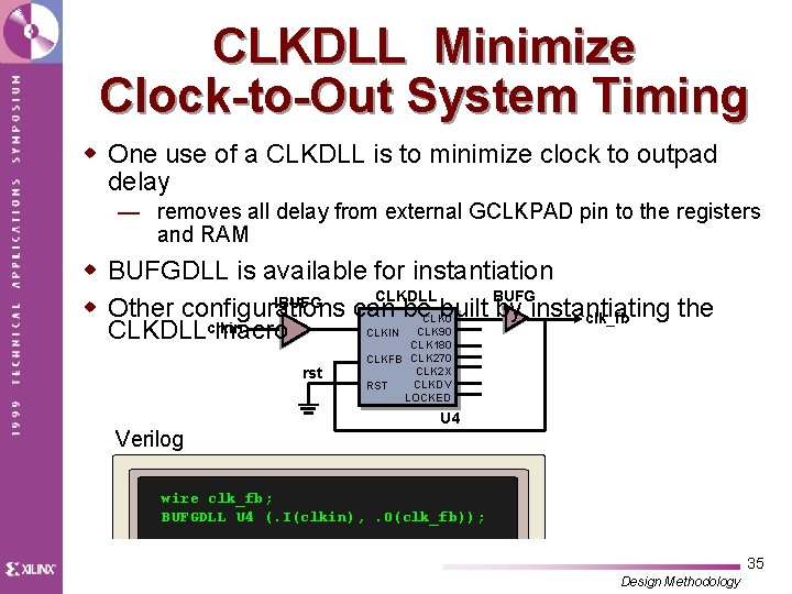
CLKDLL Minimize Clock-to-Out System Timing w One use of a CLKDLL is to minimize clock to outpad delay — removes all delay from external GCLKPAD pin to the registers and RAM w BUFGDLL is available for instantiation BUFG CLKDLL IBUFG w Other configurations can be. CLK 0 built by instantiating the clk_fb clkin CLK 90 CLKIN CLKDLL macro CLK 180 rst CLKFB CLK 270 CLK 2 X CLKDV RST LOCKED U 4 Verilog wire clk_fb; BUFGDLL U 4 (. I(clkin), . O(clk_fb)); 35 Design Methodology
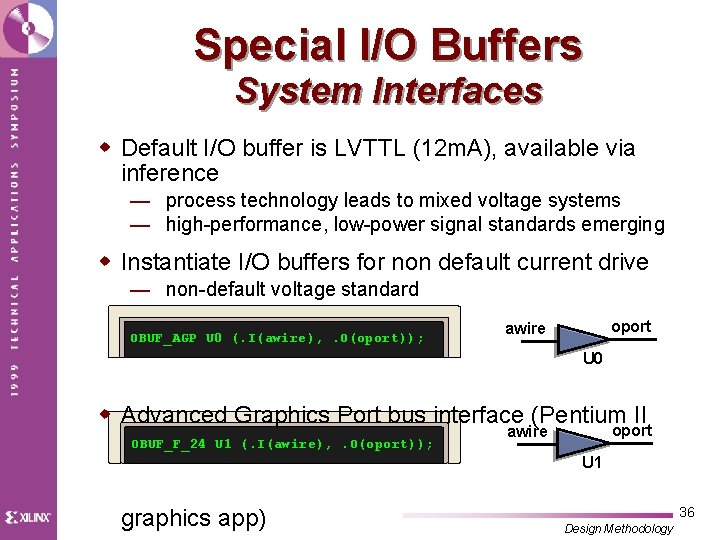
Special I/O Buffers System Interfaces w Default I/O buffer is LVTTL (12 m. A), available via inference — process technology leads to mixed voltage systems — high-performance, low-power signal standards emerging w Instantiate I/O buffers for non default current drive — non-default voltage standard — non-default slew OBUF_AGP U 0 (. I(awire), . O(oport)); oport awire U 0 w Advanced Graphics Port bus interface (Pentium II OBUF_F_24 U 1 (. I(awire), . O(oport)); oport awire U 1 graphics app) 36 Design Methodology
LUTs for Datapath Pipelining w LUT can be used in place of registers to balance pipeline stages — area efficient implementation w SRL 16 E can delay an input value up to 16 clock cycles SRL 16 E w Synchronized operands before the next operation 7 D CE CLK A 3 A 2 A 1 A 0 A[31: 0] B[31: 0] C[31: 0] G H F 8 cycles 5 cycles Z 1 cycle 12 Q 32 LUTs replace 256 registers SRL 16 E D CE CLK A 3 A 2 A 1 A 0 Q 32 LUTs replace 416 registers 37 Design Methodology
Design Verification w Trends w Stages w Xilinx solutions 38 Design Methodology
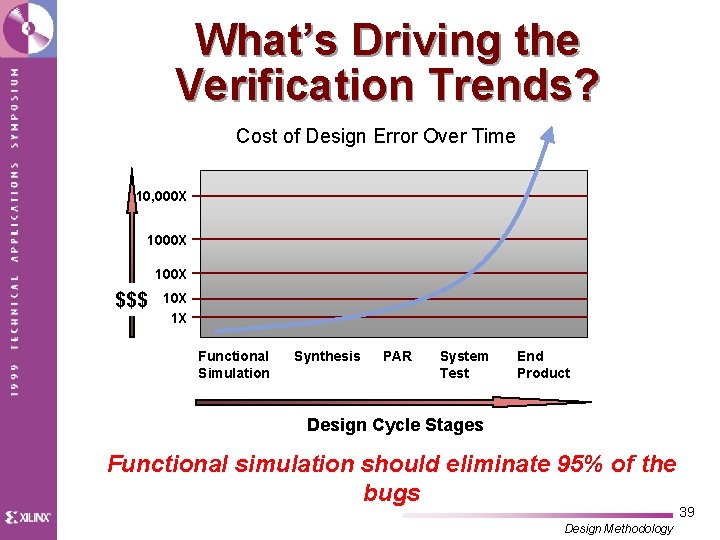
What’s Driving the Verification Trends? Cost of Design Error Over Time 10, 000 X 100 X $$$ 10 X 1 X Functional Simulation Synthesis PAR System Test End Product Design Cycle Stages Functional simulation should eliminate 95% of the bugs Design Methodology 39
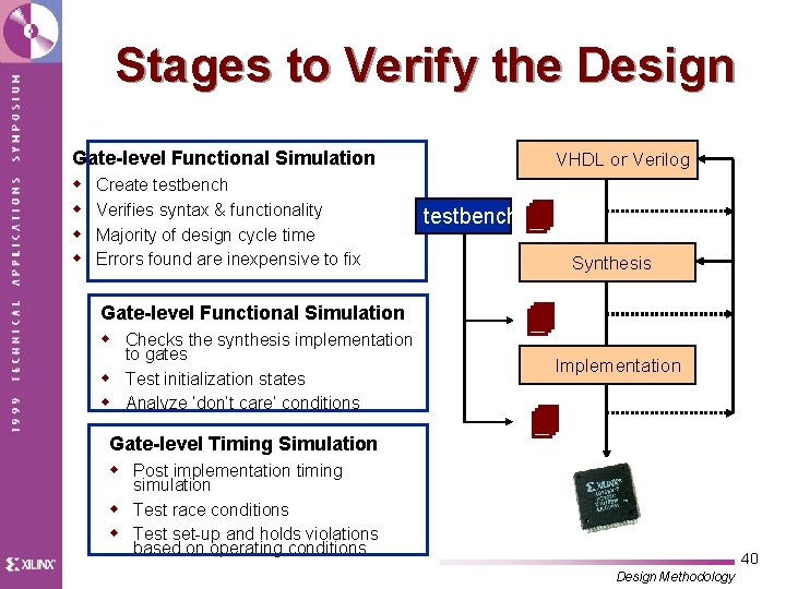
Stages to Verify the Design Gate-level Functional Simulation w w Create testbench Verifies syntax & functionality Majority of design cycle time Errors found are inexpensive to fix Gate-level Functional Simulation w Checks the synthesis implementation to gates w Test initialization states w Analyze ‘don’t care’ conditions Gate-level Timing Simulation VHDL or Verilog testbench 4 Synthesis 4 Implementation 4 w Post implementation timing simulation w Test race conditions w Test set-up and holds violations based on operating conditions 40 Design Methodology
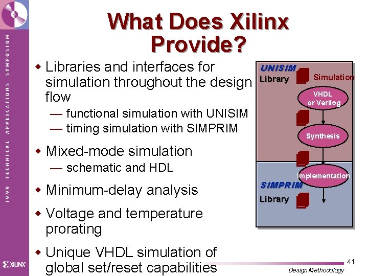
What Does Xilinx Provide? w Libraries and interfaces for simulation throughout the design flow UNISIM Library VHDL or Verilog — functional simulation with UNISIM — timing simulation with SIMPRIM 4 Synthesis w Mixed-mode simulation 4 — schematic and HDL w Minimum-delay analysis w Voltage and temperature prorating w Unique VHDL simulation of global set/reset capabilities 4 Simulation Implementation SIMPRIM Library 4 41 Design Methodology
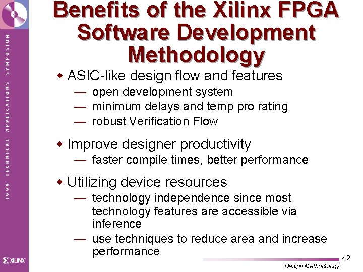
Benefits of the Xilinx FPGA Software Development Methodology w ASIC-like design flow and features — open development system — minimum delays and temp pro rating — robust Verification Flow w Improve designer productivity — faster compile times, better performance w Utilizing device resources — technology independence since most technology features are accessible via inference — use techniques to reduce area and increase performance Design Methodology 42
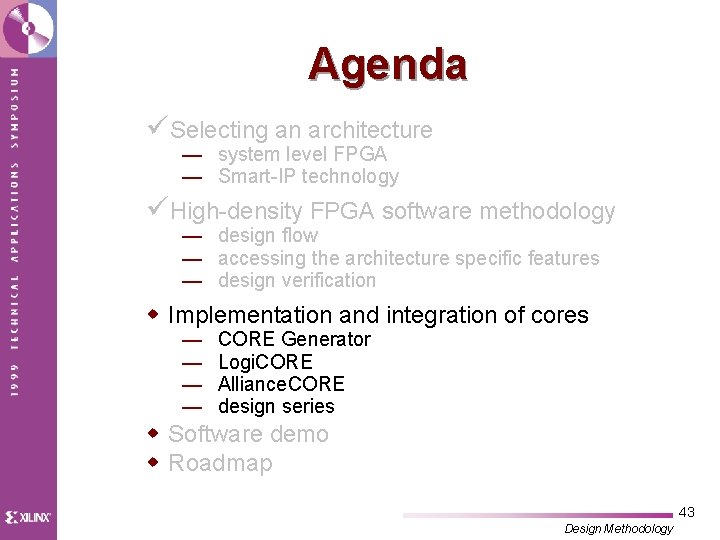
Agenda üSelecting an architecture — system level FPGA — Smart-IP technology üHigh-density FPGA software methodology — design flow — accessing the architecture specific features — design verification w Implementation and integration of cores — — CORE Generator Logi. CORE Alliance. CORE design series w Software demo w Roadmap 43 Design Methodology
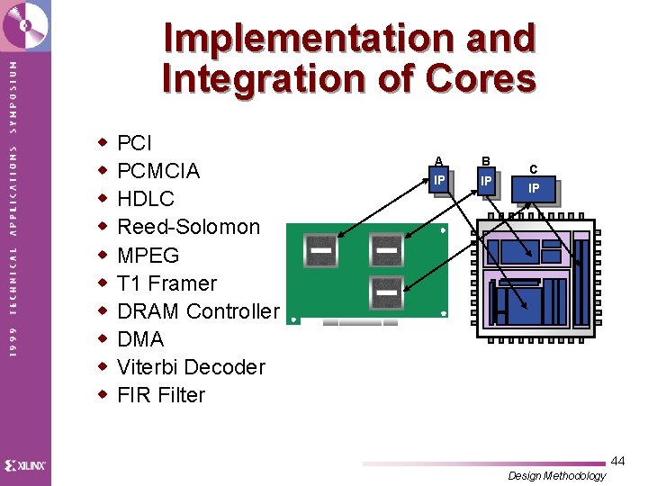
Implementation and Integration of Cores w w w w w PCI PCMCIA HDLC Reed-Solomon MPEG T 1 Framer DRAM Controller DMA Viterbi Decoder FIR Filter A B IP IP C IP 44 Design Methodology
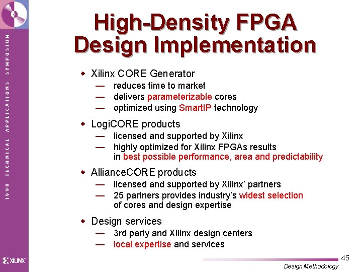
High-Density FPGA Design Implementation w Xilinx CORE Generator — reduces time to market — delivers parameterizable cores — optimized using Smart. IP technology w Logi. CORE products — licensed and supported by Xilinx — highly optimized for Xilinx FPGAs results in best possible performance, area and predictability w Alliance. CORE products — licensed and supported by Xilinx’ partners — 25 partners provides industry’s widest selection of cores and design expertise w Design services — 3 rd party and Xilinx design centers — local expertise and services 45 Design Methodology
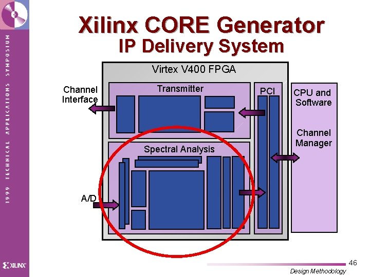
Xilinx CORE Generator IP Delivery System Virtex V 400 FPGA Channel Interface Transmitter Spectral Analysis PCI CPU and Software Channel Manager A/D 46 Design Methodology
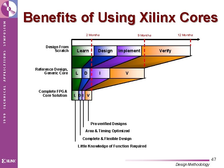
Benefits of Using Xilinx Cores 2 Months Design From Scratch Reference Design, Generic Core Complete FPGA Core Solution Learn L D Design I 12 Months 9 Months Implement Verify V L DI V Pre-verified Designs Area & Timing Optimized Complete & Flexible Design Little Knowledge of Function Required 47 Design Methodology
Benefits of Using Xilinx Cores “ 75% of all new designs will have Cores in them” - Designer feedback from IP usage survey “The high performance of the Xilinx PCI Logi. CORE solution combined with the short time to market and flexibility of a programmable FPGA solution, made Xilinx the obvious choice. " - Tony Clark, R&D Mgr. - Management Graphics, Inc “By using ‘Design Reuse’ as part of our design consulting services, on average we are able to save our customers 18 -24 weeks” - Tim Smith of Memec Design Services 48 Design Methodology
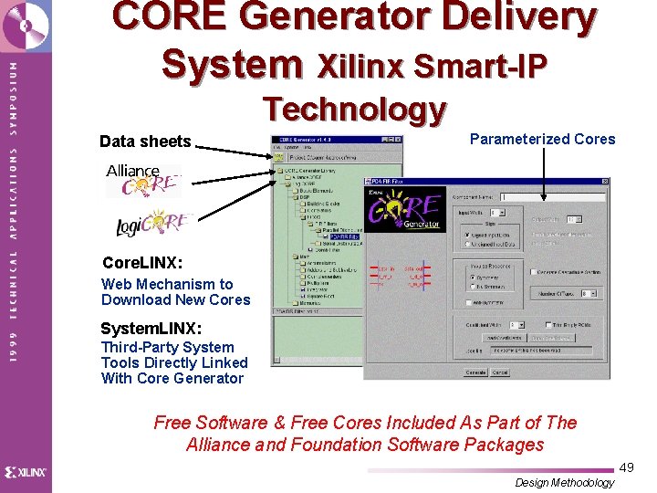
CORE Generator Delivery System Xilinx Smart-IP Technology Data sheets Parameterized Cores Core. LINX: Web Mechanism to Download New Cores System. LINX: Third-Party System Tools Directly Linked With Core Generator Free Software & Free Cores Included As Part of The Alliance and Foundation Software Packages 49 Design Methodology
Core Generator Demo 50 Design Methodology
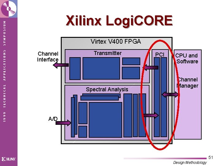
Xilinx Logi. CORE Virtex V 400 FPGA Channel Interface Transmitter Spectral Analysis PCI CPU and Software Channel Manager A/D 51 Design Methodology
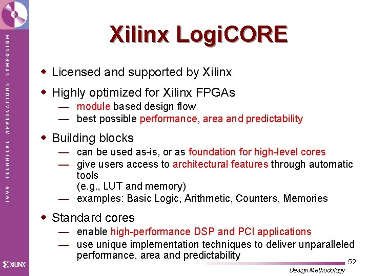
Xilinx Logi. CORE w Licensed and supported by Xilinx w Highly optimized for Xilinx FPGAs — module based design flow — best possible performance, area and predictability w Building blocks — can be used as-is, or as foundation for high-level cores — give users access to architectural features through automatic tools (e. g. , LUT and memory) — examples: Basic Logic, Arithmetic, Counters, Memories w Standard cores — enable high-performance DSP and PCI applications — use unique implementation techniques to deliver unparalleled performance, area and predictability 52 Design Methodology
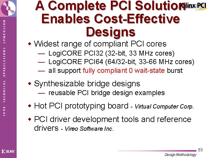
A Complete PCI Solution Enables Cost-Effective Designs w Widest range of compliant PCI cores — Logi. CORE PCI 32 (32 -bit, 33 MHz cores) — Logi. CORE PCI 64 (64/32 -bit, 33 -66 MHz cores) — all support fully compliant 0 wait-state burst w Synthesizable bridge designs — reusable PCI bridge design examples w Hot PCI prototyping board - Virtual Computer Corp. w PCI driver development tools and reference drivers - Vireo Software Inc. 53 Design Methodology
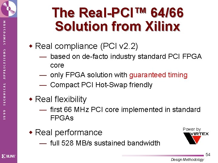
The Real-PCI™ 64/66 Solution from Xilinx w Real compliance (PCI v 2. 2) — based on de-facto industry standard PCI FPGA core — only FPGA solution with guaranteed timing — Compact PCI Hot-Swap friendly w Real flexibility — first 66 MHz PCI core implemented in standard FPGAs w Real performance Power by — full 528 MB/s sustained bandwidth 54 Design Methodology
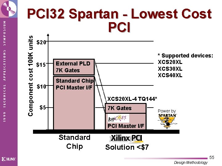
Component cost 100 K units PCI 32 Spartan - Lowest Cost PCI $20 $15 External PLD 7 K Gates $10 Standard Chip PCI Master I/F * Supported devices: XCS 20 XL XCS 30 XL XCS 40 XL XCS 20 XL-4 TQ 144* $5 7 K Gates Logic Power by PCI Master I/F Standard Chip Solution <$7 55 Design Methodology
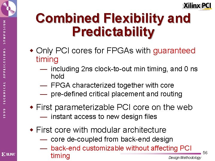
Combined Flexibility and Predictability w Only PCI cores for FPGAs with guaranteed timing — including 2 ns clock-to-out min timing, and 0 ns hold — FPGA characterized together with core — pre-defined critical placement and routing w First parameterizable PCI core on the web — instant access to new design files w First core with modular architecture — core de-coupled from back-end design — back-end customizable without affecting PCI 56 timing Design Methodology
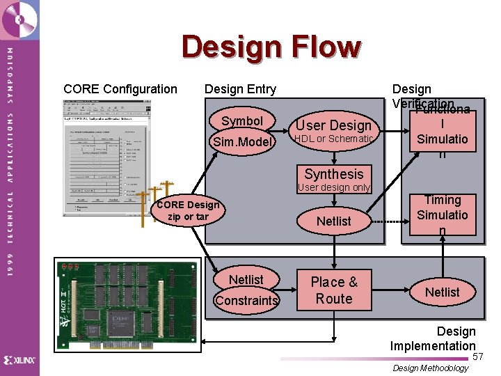
Design Flow CORE Configuration Design Entry Symbol Sim. Model Design Verification Functiona User Design HDL or Schematic l Simulatio n Synthesis User design only CORE Design zip or tar Netlist Constraints Place & Route Timing Simulatio n Netlist Design Implementation 57 Design Methodology
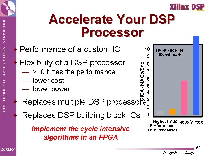
Accelerate Your DSP Processor w Performance of a custom IC — >10 times the performance — lower cost — lower power GIGA- MACs/Sec w Flexibility of a DSP processor 10 9 16 -bit FIR Filter Benchmark 8 7 6 5 4 w Replaces multiple DSP processors 32 w Replaces DSP building block ICs Implement the cycle intensive algorithms in an FPGA 1 Highest S 40 4085 Virtex Performance DSP Processor 58 Design Methodology
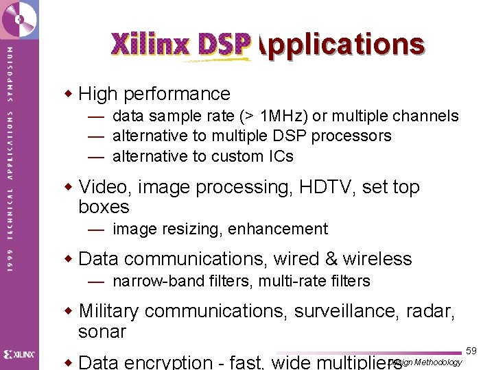
Applications w High performance — data sample rate (> 1 MHz) or multiple channels — alternative to multiple DSP processors — alternative to custom ICs w Video, image processing, HDTV, set top boxes — image resizing, enhancement w Data communications, wired & wireless — narrow-band filters, multi-rate filters w Military communications, surveillance, radar, sonar Design Methodology w Data encryption - fast, wide multipliers 59
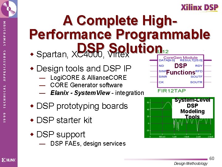
A Complete High. Performance Programmable DSP Solution w Spartan, XC 4000, Virtex w Design tools and DSP IP — Logi. CORE & Alliance. CORE — CORE Generator software — Elanix - System. View - integration w DSP prototyping boards w DSP starter kit DSP Functions System-Level DSP Modeling Tools w DSP support — DSP FAEs, design services 60 Design Methodology
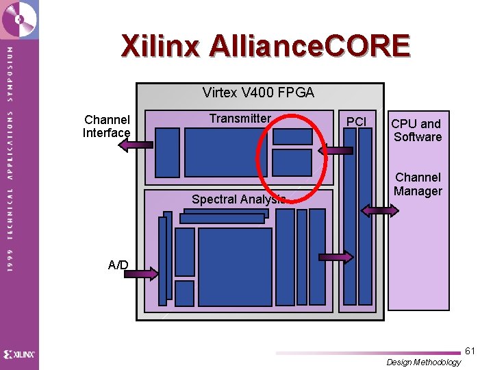
Xilinx Alliance. CORE Virtex V 400 FPGA Channel Interface Transmitter Spectral Analysis PCI CPU and Software Channel Manager A/D 61 Design Methodology
Program w Partnerships with leading third-party IP providers w Complete programmable logic solutions — proven Xilinx cores — test benches, debug software — hardware evaluation boards w License directly from partner — Xilinx netlist and source code versions — Partner guarantees functionality w Information on the Xilinx web site — www. xilinx. com/products/logicore/alliance/tblpar 62 t. htm Design Methodology
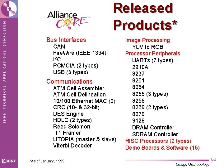
Released Products* Bus Interfaces CAN Fire. Wire (IEEE 1394) I 2 C PCMCIA (2 types) USB (3 types) Communications ATM Cell Assembler ATM Cell Delineation 10/100 Ethernet MAC (2) CRC (10 - & 32 -bit) DES Engine HDLC (2 types) Reed Solomon T 1 Framer UTOPIA (master & slave) Viterbi Decoder *As of January, 1999 Image Processing YUV to RGB Processor Peripherals UARTs (7 types) 2910 A 8237 8251 8254 8255 (3 types) 8256 8259 (2 types) 8279 9128 DRAM Controller SDRAM Controller RISC Processors (2 types) Demo Boards & Software (15) 63 Design Methodology
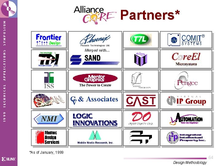
Partners* Merged with… G V & Associates *As of January, 1999 64 Design Methodology
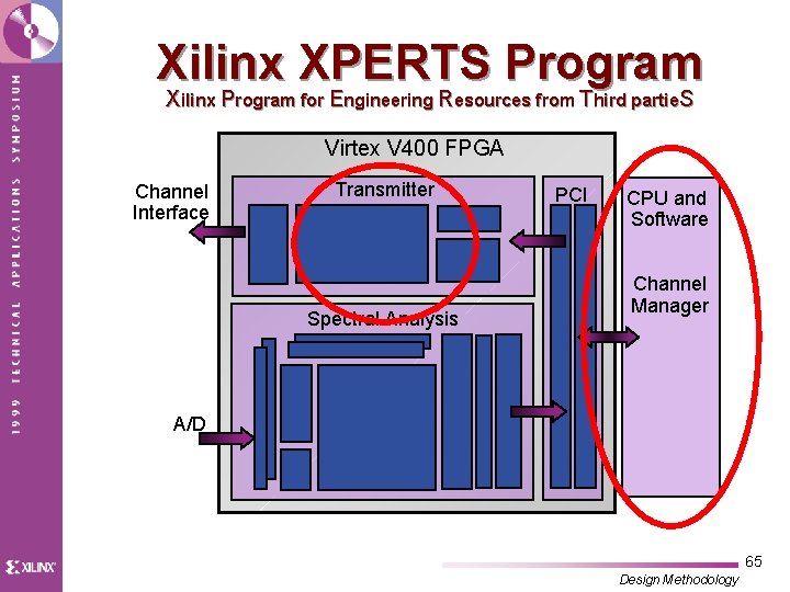
Xilinx XPERTS Program Xilinx Program for Engineering Resources from Third partie. S Virtex V 400 FPGA Channel Interface Transmitter Spectral Analysis PCI CPU and Software Channel Manager A/D 65 Design Methodology
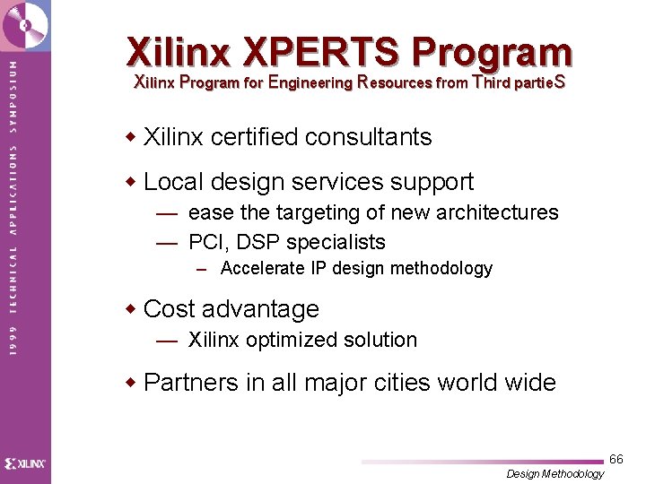
Xilinx XPERTS Program Xilinx Program for Engineering Resources from Third partie. S w Xilinx certified consultants w Local design services support — ease the targeting of new architectures — PCI, DSP specialists – Accelerate IP design methodology w Cost advantage — Xilinx optimized solution w Partners in all major cities world wide 66 Design Methodology
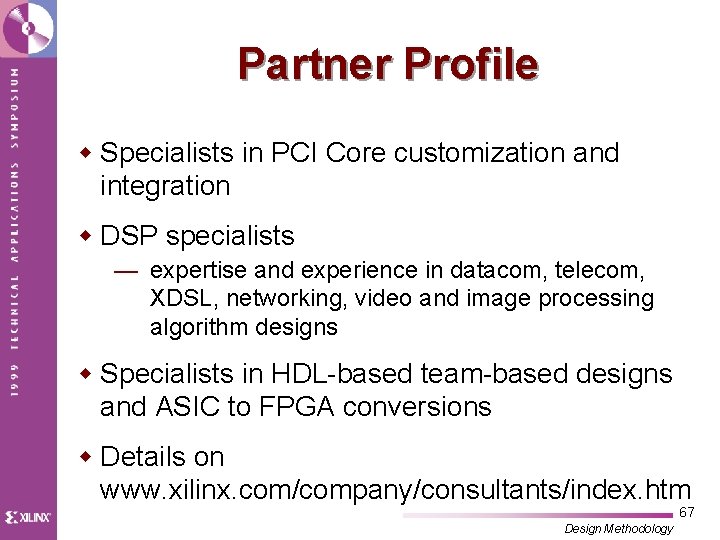
Partner Profile w Specialists in PCI Core customization and integration w DSP specialists — expertise and experience in datacom, telecom, XDSL, networking, video and image processing algorithm designs w Specialists in HDL-based team-based designs and ASIC to FPGA conversions w Details on www. xilinx. com/company/consultants/index. htm 67 Design Methodology
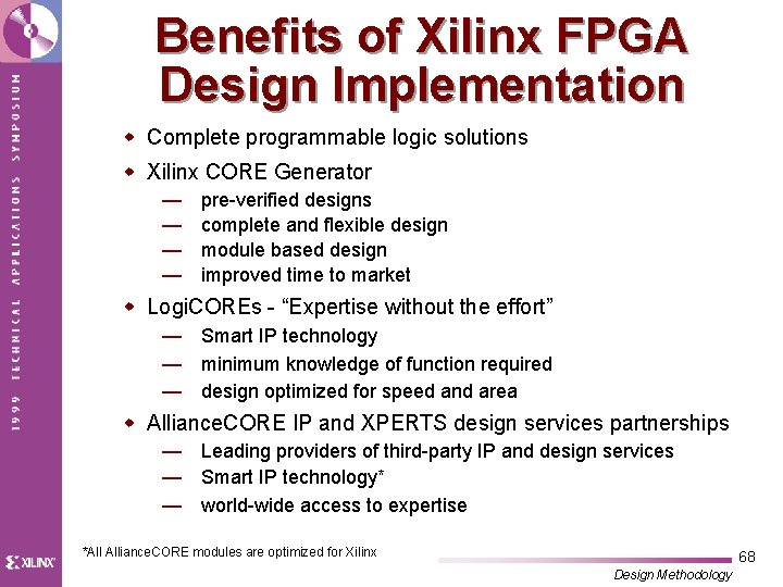
Benefits of Xilinx FPGA Design Implementation w Complete programmable logic solutions w Xilinx CORE Generator — — pre-verified designs complete and flexible design module based design improved time to market w Logi. COREs - “Expertise without the effort” — Smart IP technology — minimum knowledge of function required — design optimized for speed and area w Alliance. CORE IP and XPERTS design services partnerships — Leading providers of third-party IP and design services — Smart IP technology* — world-wide access to expertise *All Alliance. CORE modules are optimized for Xilinx 68 Design Methodology
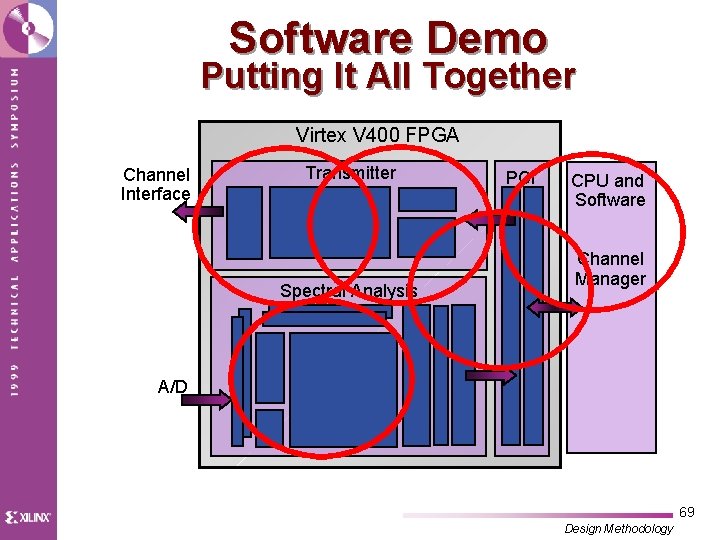
Software Demo Putting It All Together Virtex V 400 FPGA Channel Interface Transmitter Spectral Analysis PCI CPU and Software Channel Manager A/D 69 Design Methodology
Software Design Flow Demo 70 Design Methodology
Roadmap w Software w Cores w Web Access and Resources 71 Design Methodology
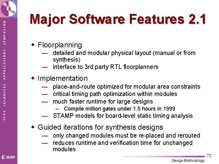
Major Software Features 2. 1 w Floorplanning — detailed and modular physical layout (manual or from synthesis) — interface to 3 rd party RTL floorplanners w Implementation — place-and-route optimized for modular area constraints — critical timing path optimization within modules — much faster runtime for large designs – Compile million gates under 1. 5 hours in 1999 — STAMP models for board-level static timing analysis w Guided iterations for synthesis designs — only changed modules must be re-placed and rerouted — reduces runtime and verification time for unchanged modules 72 Design Methodology
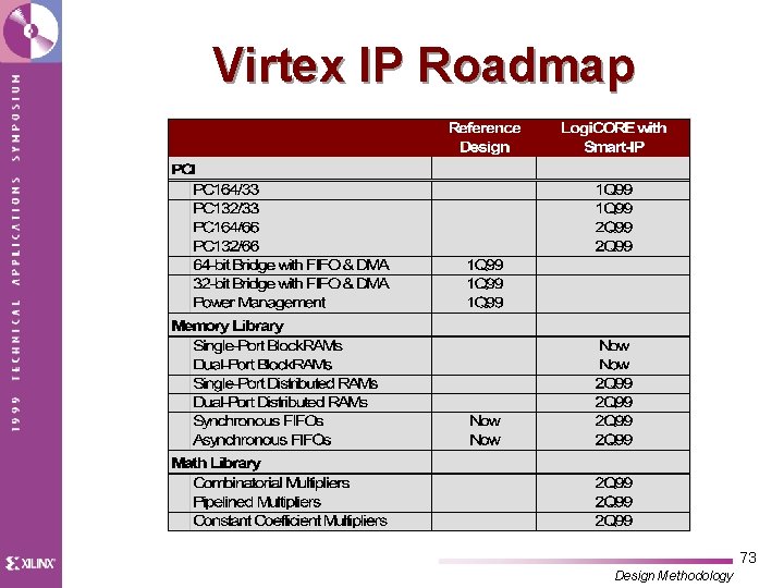
Virtex IP Roadmap 73 Design Methodology
Virtex IP Roadmap 74 Design Methodology
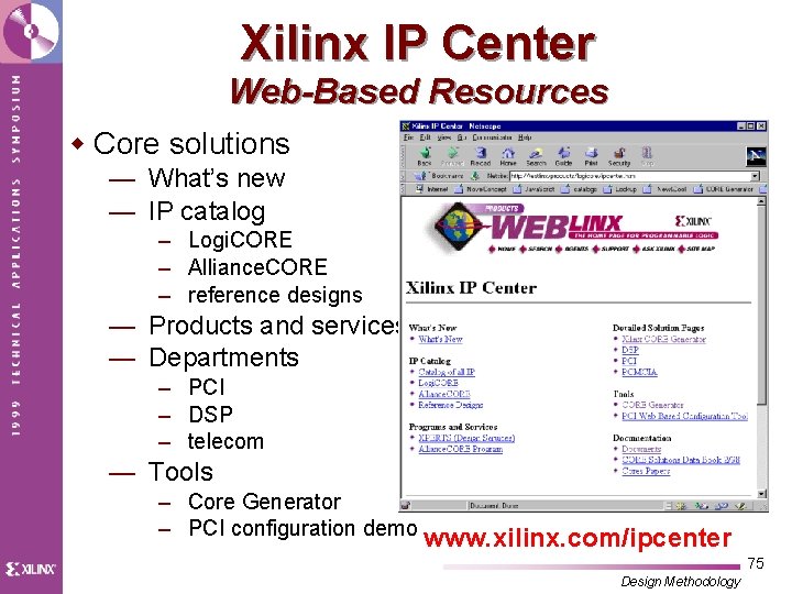
Xilinx IP Center Web-Based Resources w Core solutions — What’s new — IP catalog – Logi. CORE – Alliance. CORE – reference designs — Products and services — Departments – PCI – DSP – telecom — Tools – Core Generator – PCI configuration demo www. xilinx. com/ipcenter 75 Design Methodology
High-Density FPGA Leadership Addressing the Challenges üDevelopment platforms — Smart. IP technology - predictable, high performance, flexible — Modular design - enables “system level FPGA” — Virtex - predictable high speed, high density, fast flexible I/O, RAM üSoftware methodologies — Open development system - joint development, early access — ASIC like design flows - min delays, pro-rate temp, verification flow — Access to device resources - technology independent, optimized for Speed and area Design Methodology 76
High-Density FPGA Leadership Addressing the Challenges üDesign Implementation — Xilinx CORE Generator - Smart-IP technology, predictable, high performance, flexible, updateable from the Xilinx web site — Complete & Compliant PCI - 64/66 MHz, low cost 32/33 MHz, synthesizable bridge, prototyping boards & drivers — Complete DSP Solutions - fast, low cost, low power, slew of DSP Cores, system level tools & prototyping boards — Alliance. CORE Partnerships - focused on vertical solutions, over 25 partners, over 50 cores, verification tools & prototype boards — Multi-Level Support - expert FAE, 3 rd party consulting, 77 XPERTS, Xilinx design center Design Methodology