6 ALU Blocks and Control Contents 1 Adder

6 ALU Blocks and Control Contents 1. Adder 2. Multiplier 3. Datapath Generation 1
 A×B×C CARRY A+B+C 2")
1. Adder q Full Adder q Boolean equation Sum(Odd Parity) A×B×C CARRY A+B+C 2

Which is better? q Boolean Equation 1 : q Boolean Equation 2 : q CARRY evaluation is more urgent since CARRY is in the critical path S 0 C 0 S 1 ADDER A 0 B 0 C 1 S 2 ADDER A 1 B 1 C 2 Sn ADDER A 2 B 2 Cn ADDER An Cn Bn [ Ripple Carry Adder ] 3

Alternating Complementary Form q At Odd Stages A B C SUM q At Even Stages CARRY A B C CARRY SUM A B C SUM CARRY 4

Alternating Complementary Form 5

Dynamic Serial Adder A A SUM B B CARRY C S R/S Q D CLOCK 6

Dynamic Configuration CARRY GATE SUM GATE CK CK A OPTIONAL PRECHARGE DEVICE C B A B A B CK CK SUM C S R CK CK Set/Reset Circuit C (CARRY) R S 7

Full Adder Truth Table 0 1 2 3 4 5 6 7 A B C 0 0 1 1 0 1 0 1 CARRY SUM 0 0 0 1 1 1 0 1 0 0 1 Mutually Complement 0 7 1 6 2 5 3 4 FC - on terms FS - on terms q Conjugate Symmetry 8

Another Configuration of Carry & Sum Logic 1 PROPAGATE A B A C CARRY A 1 PROPAGATE A 1 GENERATE B CARRY STAGE 1 GENERATE A B C CARRY A B C C B A SUM STAGE 9

Dynamic full adder using np CMOS logic style 10

Layout of the dynamic full adder 11

Looking at the FA Truth Table A B C 0 0 1 1 0 1 0 1 CARRY SUM 0 0 0 1 1 1 0 1 0 0 1 12

Transmission Gate Implementation C C A B SUM A B B A B CARRY C 13
 C 0 P 1 G 1 P 2 C 1")
CLA (Carry Lookahead Adder) C 0 P 1 G 1 P 2 C 1 An Gn Bn Pn C 2 G 2 P 3 C 3 G 3 P 4 C 4 G 4 14

Carry bypass structure - basic concept 15
-bit carry bypass adder(each stage: M bits) q tp = tsetup + M *")
(N=16)-bit carry bypass adder(each stage: M bits) q tp = tsetup + M * tcarry+(N/M - 1) tbypass + M*tcarry+tsum l tsetup : time to create G and P signals l tcarry : propagation delay through a single bit l tbypass : propagation delay through MUX l tsum : time to generate sum 16
 CK G")
Combining 4 Domino Carry Lookahead Blocks q Manchester Carry Chain (4 -bit) CK G 1 P 1 G 2 P 2 G 3 P 3 G 4 P 1 C 0 P 2 C 1 G 1 P 3 C 2 G 2 P 4 C 3 G 3 C 4 G 4 C 0 MANCHESTER CARRY CHAIN C 4 CK C 0 C 1 C 2 C 3 C 4 q Limit @ 4 stages u In the worst case, 6 Series Tr. s to the ground. 17

Improving Worst Case Carry Prop. Time MANCHESTER CARRY CHAIN C 0 P 1 C 4 CK P 2 P 3 P 4 CK 18

Manchester CC Adder Floorplan A 4 B 4 GP BIT 3 A 3 B 3 GP BIT 2 A 2 B 2 GP BIT 1 A 1 B 1 SUM GENERATE q Dual CC Scheme MANCHESTER CARRY CHAINCARRY CHAIN BIT 4 MANCHESTER CARRY CHAINCARRY CHAIN C 4 l SUM S 4 SUM S 3 SUM S 2 SUM GENERATE S 1 l One for Carry Prop. The other for off-loading the 1 st CC from the SUM -block. C 0 19
 Realization of MUX with restoring logic A 4 ~ A")
CSA (Carry Select Adder) Realization of MUX with restoring logic A 4 ~ A 7 B 4 ~ B 7 1 S 4 1 ~ S 7 1 C 8 A 4 ~ A 7 B 4 ~ B 7 0 S 4 0~ S 7 0 Carry Selection 1 1 0 S 4 ~ S 7 C 8 0 C 8 Note) Realization of MUX with pass-transistor gates C 4 C 8 0 0 A 0 ~ A 3 B 0 ~ B 3 C 0 S 0 ~ S 3 C 8 C 4 1 C 80 C 81 C 4 S 0 ~ S 3 Vdd C 8 C 120 C 121 C 8 C 12 C 8 Vdd - Vt Vdd - 2 Vt Threshold voltage loss per stage 20
 q For carry propagation, use restoring logic in the alternative")
CSA (Carry Select Adder) q For carry propagation, use restoring logic in the alternative pattern A 0 ~ A 3 B 0 ~ B 3 C 0 S 0 ~ S 3 C 4 C 8 0 C 8 1 C 120 C 121 C 8 Number of bits for each stage ex 1) 32 -bit case : 4, 4, 5, 6, 7, 6 ( or 4, 4, 5, 6, 6, 7) ex 2) 64 -bit case : 4, 4, 5, 6, 7, 8, 9, 10 21

Minimization of Carry Propagation Path Delay q Carry Select Scheme (prepare result for each case, Cin=1, Cin=0) q Simplify the carry selection using the characteristic between Ci 0 & Ci 1 q Take complement carries alternating the Even and Odd stages q Adjust each block size with the consideration to the delay of carry select logic l carry propagation delay of each block = = carry propagation delay to the block adjust eg. for 32 -bit path 4 4 5 6 6 7 22
 q tadd = tsetup + M * tcarry+")
16 -bit Linear CSA(Carry Select Adder) q tadd = tsetup + M * tcarry+ (N/M ) tmux + tsum M: #of bits/stage N : total # of bits 23

Square Root CSA q tadd = tsetup + M * tcarry+ 2 N tmux + tsum l N = M + (M+1) + …. . + (M+P-1) = MP + P(P-1)/2 = P 2/2 + P(M - 1/2 ) 9 stage 24

Propagation Delay of Linear and Square Root CSA and linear RCA 25

Carry Skip Adder q Ripple Carry Adder와 CLA Adder의 Compromise a 15 b 15 a 13 b 13 a 14 b 14 a 12 b 12 c 16 G 12, 15 a 3 b 3 a 1 b 1 a 2 b 2 a 0 b 0 c 12 G 8, 11 P 12, 15 c 8 P 8, 11 G 4, 7 c 4 c 0 P 4, 7 26

pi’s and gi’s are computed from pi=ai bi and gi = ai bi Initially, c 4, c 8 and c 12 are cleared After 4 clock cycle (at T 0+4 Tc), G-values are calculated as cout assuming ci=0(P-values are also calculated by then) At this time (at T 0+4 Tc), true cout in the first stage, c 4 is obtained. After one, two and three clock cycles respectively, assuming the delay of each AOI gate as Tc true values of c 8, c 12 and c 16 are obtained. Sum and cout of the last block are obtained at (T 0+4 Tc+2 Tc+4 Tc) 27

Comparison of Carry Select & Carry Skip Adder q A 32 -bit Carry Select Adder Stage # bits/stage inc. delay 1 2 3 4 5 6 4 4 5 6 7 6 4 1 1 1 q A 32 -bit Carry Skip Adder Stage # bits/stage inc. delay 1 2 3 4 5 6 7 8 2 4 1 1 2 32 bit 9 k 2(k 2=delay due to 1 -bit addition or MUX) 10 k 2 28

Conditional Sum Adder A 2 B 2 A 1 B 1 A 0 B 0 S 2 1 C 3 1 S 2 0 C 3 0 S 1 1 C 2 1 S 1 0 C 2 0 S 0 1 C 1 1 S 0 0 C 1 0 MPX MPX S 2 (C 1=1) C 3 (C 1=1) S 1 (C 1=1) C 3 S 2 (C 1=0) S 1 (C 1=0) C 3 S 0 C 1 Triple 2 -input MUX S 2 C 0 S 1 29

Carry Lookahead Tree Adder q Previous CLA implementation is not very adequate due to fan-in, fan-out problem & irregularity, despite the small(5) number of logic levels. l Make it regular, using log 2 n - logic levels. a 3 b 3 g 3 p 3 G 2, 3 P 2, 3 a 2 b 2 g 2 p 2 a 1 b 1 g 1 p 1 a 0 b 0 g 0 p 0 G 0, 1 P 0, 1 ai bi gi pi Gj+1, k Pj+1, k G 0, 3 P 0, 3 Gi, k Pi, k Gi, j Pi, j [ 1 st Part ] 30

Carry Lookahead Tree Adder C 3 C 2 g 2 p 2 C 2 G 0, 1 P 0, 1 C 3 Cj+1 g 0 p 0 Ci Gi, j Pi, j C 0 Ci [ 2 nd Part ] C 0 S 3 a 3 b 3 C 0 S 2 a 2 b 2 C 2 S 1 a 1 b 1 C 1 S 0 a 0 b 0 C 0 C 0 S 3 aibi gi pi C i Gj+1, k Pj+1, k Cj+1 Gi, k [ Complete CLA Tree Adder ] Gi, j Pi, k Ci Ci 31

Carry Save Adder q Ripple Carry Adder q Carry Lookahead Adder q CSA (Conditional Sum Adder) Carry Propagate Adder q CSA (Carry Select Adder) q CSA (Carry Skip Adder) q CSA (Carry Save Adder) 32

Carry Save Adder q Carry Save Adder is used wherever a large number of operands have to be added. Previous Cycle Sum Operand Previous Cycle Carry F. A F. A CSA stages F. A F. A Carry Sum F/F F. A aibici CPA 33

2. Multiplier q Add-and-Shift Algorithm + 0 0 1 1 multiplicand 1 0 multiplier 0 0 0 0 + 0 0 1 1 0 + 0 0 0 0 0 0 0 1 1 0 0 0 0 1 1 1 0 10 0 1 1 0 Multiplication procedure by Pencil-and-Paper Method by Add-and-Shift Algorithm 34

The Serial-Parallel Multiplier A B D a 3 a 2 a 1 a 0 D D D D b 2 D b 1 D F. A F. A b 0 D D D D 0 Output 35

4 x 4 array multiplier 36
![N(4) M(3) q tmult = [(M-1) + (N-1)] * tcarry + (N-1) * tsum+](http://slidetodoc.com/presentation_image_h2/5e7677ca20f6b5c7218927aedb96ee34/image-37.jpg "N(4) M(3) q tmult = [(M-1) + (N-1)] * tcarry + (N-1) * tsum+")
N(4) M(3) q tmult = [(M-1) + (N-1)] * tcarry + (N-1) * tsum+ tand l both tcarry and tsum are important l Sum and Carry generation time need to be similar. 37
 Rectangular floorplan of CSM 38")
Carry-save Multiplier(CSM) Rectangular floorplan of CSM 38
 q Booth Encoder Table q Booth Encoder b 2")
The Modified Booth Algorithm (cont’) q Booth Encoder Table q Booth Encoder b 2 k+1 b 2 k-1 multiplied by 0 0 0 1 +x 0 1 0 +x 0 1 1 + 2 x 1 0 0 - 2 x 1 0 1 -x 1 1 0 -x negative 1 1 1 0 = b 2 k+1 b 2 k-1 b 2 k A = b 2 k-1 2 A b 2 k+1 39

Booth Multiplication Example A 01 00 01 17 X 11 01 11 -9 -A +2 A -A Operation 00 00 00 10 11 11 11 10 00 10 01 11 00 01 11 10 11 11 11 01 10 01 11 Initial 0 Add -A + 2 -bit Shift Add 2 A + 2 -bit Shift Add -A + 11 -153 40

The Modified Booth Algorithm q Let’s consider a number B = (bn-1, bn-2, . . . , b 1, b 0) written in 2’scomplement. q B may be rewritten as follows : l Example q In this equation, the terms in brackets is in the set {-2, -1, 0, 1, 2} q n-bit multiplier generates exactly n/2 partial products 41

Parallel Multiplier q Multiplier has two basic operations l The generation of partial products l The summation of partial products q Parallel multiplier avoids the overhead that is due to the separate controls of these two operations q We speed up the multiplication q The gain in speed is obtained at the expense of extra hardware q Parallel multiplier can be implemented so as to support a high rate of pipelining 42

The Braun Multiplier q A straightforward implementation l One bit of the new partial product ( ai l l a 1 a 0 b 3 b 2 b 1 b 0 a 3 b 1 a 2 b 1 a 1 b 1 a 0 b 1 j) Carry in a 2 a 3 b 0 a 2 b 0 a 1 b 0 a 0 b 0 . b One bit of the previous partial product a 3 b 2 a 2 b 2 a 1 b 2 a 0 b 2 a 3 b 3 a 2 b 3 a 1 b 3 a 0 b 3 P 6 P 5 P 4 P 3 P 2 P 1 P 0 q In the first four rows there is no horizontal carry propagation (using carry-save adder) 43
 a 3 a 2 a 1 a 0 b 0")
The Braun Multiplier (cont’) a 3 a 2 a 1 a 0 b 0 0 F. A F. A p 0 F. A 0 p 7 F. A p 6 p 5 p 4 p 1 p 2 b 1 b 2 b 3 p 3 44

Baugh-Wooley Multiplier q Modified in order to allow multiplication of signed number q Let’s consider 2 number A and B (2’s complement number) q The product A. B is 45
 a 3 a 2 a 1 a 0 b 0 0")
Baugh-Wooley Multiplier (cont’) a 3 a 2 a 1 a 0 b 0 0 F. A 1 F. A F. A p 7 p 6 p 5 p 4 p 0 p 1 p 2 b 1 b 2 b 3 a 3 b 3 F. A p 3 46

Wallace Tree Multipliers q Full adder vs Wallace tree 20 20 Full Adder 21 20 20 20 Wallace n 2 n 21 20 q Useful whenever a large number of operands are to add. q Completion time in Braun or Baugh-Wooley multiplier l Using Ripple Carry Adder: Proportional to the twice number of n of bits l Using Wallace trees, Proportional to log 2 (n) 47

Recursive Decomposition of the Multiplication q Partitioning two operands q Four Terms (AH. BH, AH. BL, AL. BH, AL. BL) are computed using 4 p-bits multipliers q The results are collected through Wallace tree 48

Recursive Decomposition of the Multiplication AH X AL BH BL AL X BL AH X BL AL X BH AH AL AL X AH X BH BL AL X BL BH BH BH AH X AH BH AL X AH X BL AL X BL BH 4 X W 3 BL 4 X W 3 Adder Aligning the four partial products 49

Booth’s Algorithm Array Multiplication q Another approach to the design of a parallel multiplier for two’s complement operands q The basic cell in rows i perform an add, subtract or transfer-only q CASS (Controlled Add/Subtract/Shift) Cell a Pin (partial product) H D cout cin 50
 x 3 CTRL x 2 CTRL x 1 x")
Booth’s Algorithm Array Multiplication (cont’) x 3 CTRL x 2 CTRL x 1 x 0 0 a 3 H D 0 0 a 2 a 1 0 a 0 0 CASS H D CASS CASS CASS CTRL H D CASS CASS P 6 P 5 P 4 P 3 P 2 P 1 P 0 Xi Xi-1 0 1 1 0 0 Shift 1 Shift 0 Subtract 1 Add 0 0 0 H D 0 0 1 1 d d 1 0 51

Generalized block diagram of an array multiplier 52

Q. Why use an array multiplier if it requires as many addition steps? A 1) Array multiplier is combinational circuit, where the signals flow without being clocked. Multi-pass Array Multiplier : normally use a clock, but the cycle time for passing through k arrays is < k. Tc 53
 Some speed-up schemes are possible. e. g. E/O array, Wallace-tree q Even-Odd")
A 2) Some speed-up schemes are possible. e. g. E/O array, Wallace-tree q Even-Odd Array 54

q Wallace-tree Multiplier 55

q 6 x 6 Wallace-tree Multiplier Example q (n : width of the Wallace tree) e. g. For 32 -bit, number of adders necessary for each stage is 32 - 22 - 16 - 12 - 8 - 6 - 4 - 3 - 2 Total delay = 9 x adder delay 56

57

3. Datapath Generation Datapath and its elements in bit-slice organization INPUT-OUTPUT MEMORY CONTROL DATAPATH 58

Two layout strategies for bit-slice datapath 59
 60")
Layout of 4 -bit DP using layout strategy II (feedthrough) 60

1 -D placement vs. 2 -D placement 61
 62")
1 -D placement vs. 2 -D placement(Cont’) 62

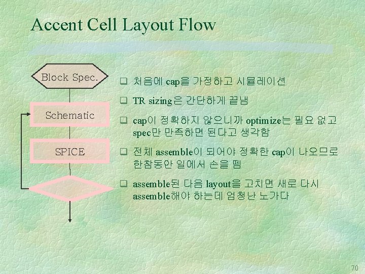
Datapath Layout Flow RTL description Floorplan Schematic Drawing Cell Drawing q circuit design l floorplan : block ordering, bus track assignment l schematic drawing : tr. sizing q layout l cell drawing : leaf cell layout assemble : leaf cell integration (routing) Layout Assemble DRC / LVS l Back-Annotation Datapath Layout DRC / LVS : design rule check, layout vs. schematic q back-annotation l simulation with the exact capacitance 63
 q real mode support of x 86 instruction")
Datapath Design Case (ACCENT HK 386) q real mode support of x 86 instruction set q enhanced (pipelined) datapath q problems & practices of general DP layout 64
 l barallel shifter(40 bit) l segment/effective address(32")
Datapath structure l alu, register file(32 bit) l barallel shifter(40 bit) l segment/effective address(32 bit) Segment, EA q 3 major blocks Barrel Shifter ALU Register File 65
 metal 2 Control, Clock Power N-well P-well")
Track capacity metal 1 VSS VDD TRACK(6) metal 2 Control, Clock Power N-well P-well q 6 vertical wires/track in metal 1 l metal 3 reserved for P & G routing 66
 q Considering IR drop Segment, EA BSH ALU")
q From bottom & left(chip edges) q Considering IR drop Segment, EA BSH ALU Power Grid RF 67

Cell Structure q Initial cell template decision 70 80 N-well P-well l Nwell in the left l Pwell in the right l data flow vertical l control flow horizontal l Similar cell structure as VTI l Cell width – 80 for PMOS – 70 for NMOS 25 10 35 45 10 25 68

Cell Structure q 모든 쎌에 power line이 통과함 q power line width 10 (2 contact) q power line location 25 to the inside from the boundary 69
 q Using 45 degree line for cell design Control flow Data flow")
Cell Design(I) q Using 45 degree line for cell design Control flow Data flow 71
 q needless effort to reduce cell size l ugly poly; current crowding")
Cell Design(II) q needless effort to reduce cell size l ugly poly; current crowding Data flow 72

q Critical path used for transistor sizing in relevant datapath element 73

Assemble Data flow • Track assignment needs to be done before the cell layout (not after). 74

- Slides: 76