
Datapath Components for Lab The Processor 4 1
Datapath Components for Lab The Processor! (4. 1 - 4. 4 4 th ed) 2/14 Cpu control. 1
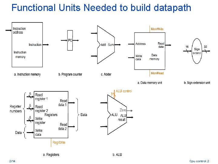
Functional Units Needed to build datapath 2/14 Cpu control. 2
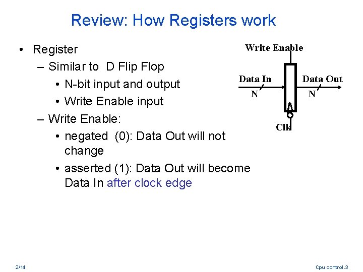
Review: How Registers work Write Enable • Register – Similar to D Flip Flop Data In Data Out • N-bit input and output N N • Write Enable input – Write Enable: Clk • negated (0): Data Out will not change • asserted (1): Data Out will become Data In after clock edge 2/14 Cpu control. 3
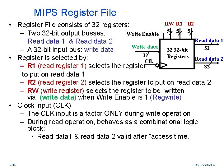
MIPS Register File RW R 1 R 2 • Register File consists of 32 registers: 5 5 5 – Two 32 -bit output busses: Write Enable Read data 1 & Read data 2 Write data 32 32 32 -bit – A 32 -bit input bus: write data 32 Registers Read data 2 • Register is selected by: Clk – R 1 (read register 1) selects the register 32 to put on read data 1 – R 2 (read register 2) selects the register to put on read data 2 – RW (write register) selects the register to be written via (write data) when Write Enable is 1 (Regwrite) • Clock input (CLK) – The CLK input is a factor ONLY during write operation – During read operation, behaves as a combinational logic block: • Read data 1 & read data 2 valid after “access time. ” 2/14 Cpu control. 4
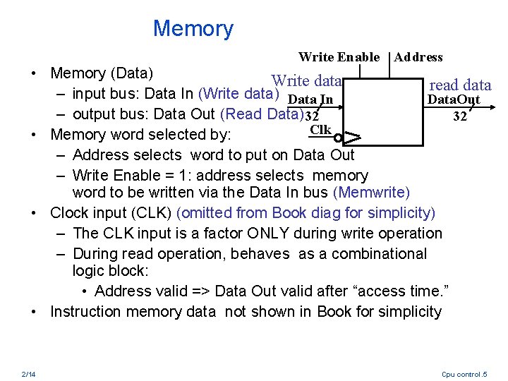
Memory Write Enable Address • Memory (Data) Write data read data – input bus: Data In (Write data) Data In Data. Out – output bus: Data Out (Read Data)32 32 Clk • Memory word selected by: – Address selects word to put on Data Out – Write Enable = 1: address selects memory word to be written via the Data In bus (Memwrite) • Clock input (CLK) (omitted from Book diag for simplicity) – The CLK input is a factor ONLY during write operation – During read operation, behaves as a combinational logic block: • Address valid => Data Out valid after “access time. ” • Instruction memory data not shown in Book for simplicity 2/14 Cpu control. 5
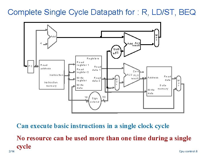
Complete Single Cycle Datapath for : R, LD/ST, BEQ M u x Ad d A LU result 4 S hift left 2 PC R ea d ad dres s Instru c tio n Instruc tion m e m ory R egiste rs R ead register 1 R ea d R e ad da ta 1 re gister 2 W rite register R ea d da ta 2 M u x W rite d ata Z ero A LU A L U resu lt A ddre ss W rite da ta 16 S ig n extend R e ad d ata D ata m em ory M u x 32 Can execute basic instructions in a single clock cycle 2/14 No resource can be used more than one time during a single cycle Cpu control. 6
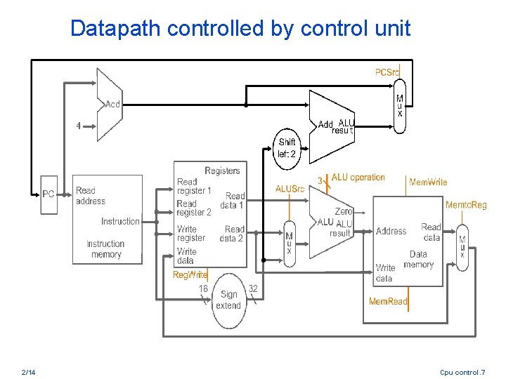
Datapath controlled by control unit 2/14 Cpu control. 7
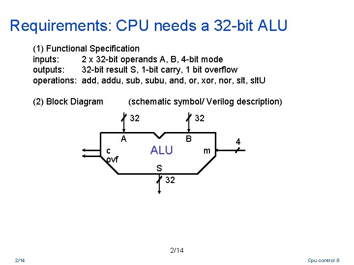
Requirements: CPU needs a 32 -bit ALU (1) Functional Specification inputs: 2 x 32 -bit operands A, B, 4 -bit mode outputs: 32 -bit result S, 1 -bit carry, 1 bit overflow operations: add, addu, subu, and, or, xor, nor, slt. U (2) Block Diagram (schematic symbol/ Verilog description) 32 A c ovf 32 ALU B m 4 S 32 2/14 Cpu control. 8
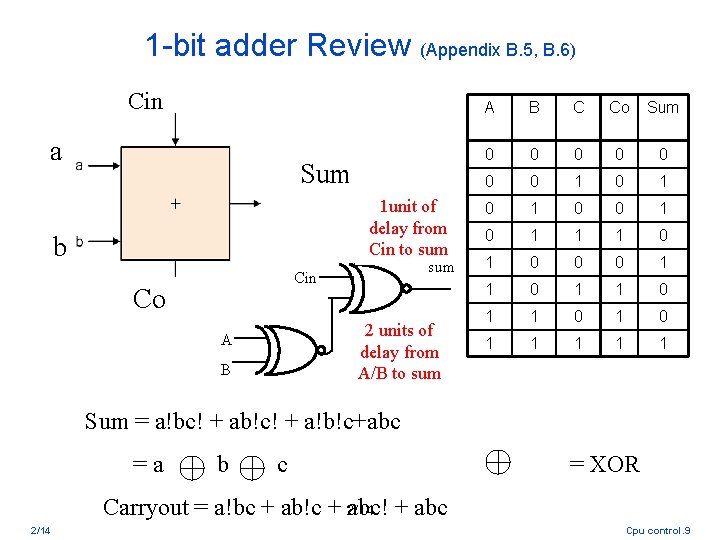
1 -bit adder Review (Appendix B. 5, B. 6) Cin a Sum 1 unit of delay from Cin to sum b sum Cin Co 2 units of delay from A/B to sum A B C Co Sum 0 0 0 0 1 0 1 0 1 1 1 0 0 0 1 1 0 1 1 1 Sum = a!bc! + ab!c! + a!b!c+abc =a b c = XOR Carryout = a!bc + ab!c + 2/14 abc! + abc 2/14 Cpu control. 9
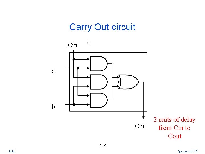
Carry Out circuit Cin a b 2 units of delay Cout from Cin to Cout 2/14 Cpu control. 10
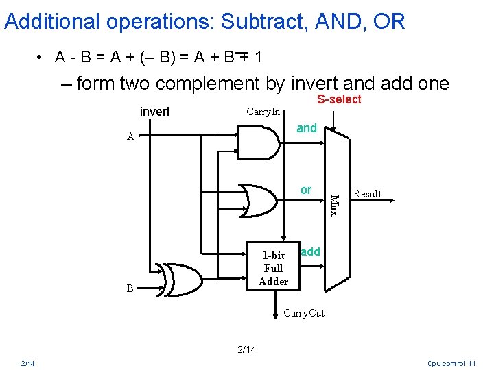
Additional operations: Subtract, AND, OR • A - B = A + (– B) = A + B + 1 – form two complement by invert and add one invert S-select Carry. In and A 1 -bit Full Adder B Mux or Result add Carry. Out 2/14 Cpu control. 11
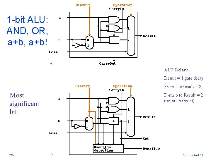
Binvert 1 -bit ALU: AND, OR, a+b! Operation Carry. In a 0 1 b Result 0 2 1 Less 3 a. Carry. Out ALU Delays Result = 1 gate delay Binvert Most significant bit From a to result = 2 Operation Carry. In a Form b to Result = 2 (ignore b invert) 0 1 b Result 0 2 1 Less 3 Set Overflow 2/14 detection 2/14 b. Overflow Cpu control. 12
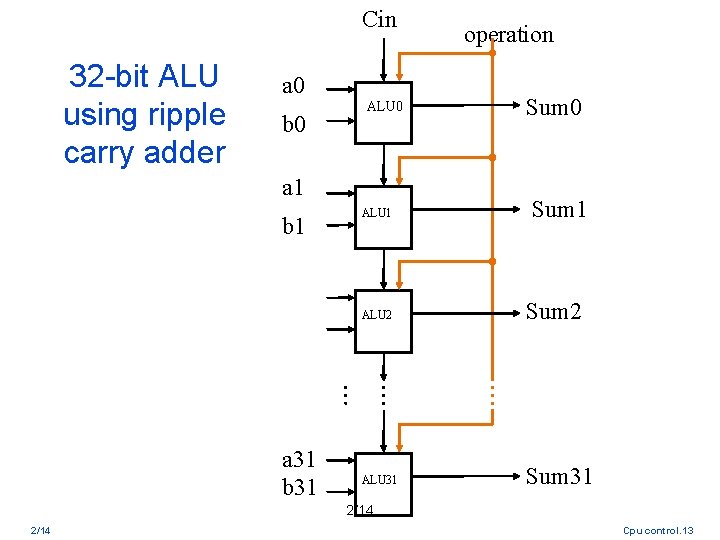
Cin 32 -bit ALU using ripple carry adder a 0 b 0 ALU 0 a 1 b 1 a 31 b 31 ALU 1 operation Sum 0 Sum 1 ALU 2 Sum 2 ALU 31 Sum 31 2/14 Cpu control. 13
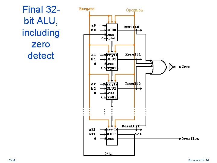
Final 32 bit ALU, including zero detect Bnegate a 0 b 0 Operation ALU 0 Less Result 0 Carry. Out a 1 b 1 0 Carry. In ALU 1 Less Carry. Out Result 1 a 2 b 2 0 Carry. In ALU 2 Less Carry. Out Result 2 a 31 b 31 0 Carry. In ALU 31 Less Zero Result 31 Set Overflow 2/14 Cpu control. 14
- Slides: 14