Hardware Design of an Arithmetic Logic Unit ALU



- Slides: 16

Hardware Design of an Arithmetic Logic Unit (ALU) Felix Noble Mirayma V. Rodriguez Agnes Velez University of Puerto Rico Mayagüez Campus Mayagüez, Puerto Rico Department of Electrical and Computer Engineering

Outline • • Introduction ALU Design – – • • Full Adder A input device B input device Logical Operation Device Conclusion Future Work References Acknowledgements

Introduction – An arithmetic-logic unit (ALU) is the part of a computer processor (CPU) that carries out arithmetic and logic operations on the operands in computer instruction words. – The ALU includes storage places for input operands, operands that are being added, the accumulated result (stored in an accumulator), and shifted results. The flow of bits and the operations performed on them in the subunits of the ALU is controlled by gated circuits.

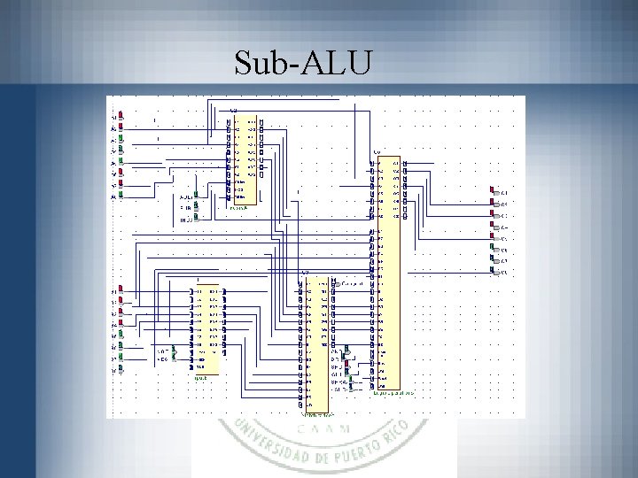
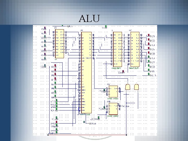
ALU Design – The ALU is a combinational circuit that continuously computes its outputs as a function of its inputs. A change in its inputs will produce valid outputs by the strobe time of the current clock cycle. – This ALU uses only one bus and consist of a full adder, two inputs, A and B, and a logical device, which is the part in charge of the ands, ors, and shifts.

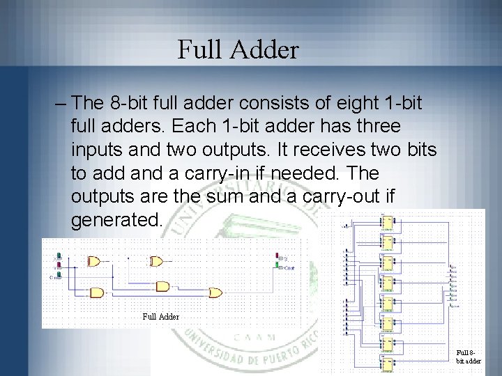
Full Adder – The 8 -bit full adder consists of eight 1 -bit full adders. Each 1 -bit adder has three inputs and two outputs. It receives two bits to add and a carry-in if needed. The outputs are the sum and a carry-out if generated. Full Adder Full 8 bit adder

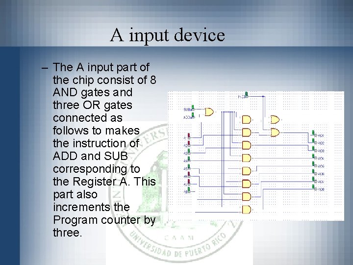
A input device – The A input part of the chip consist of 8 AND gates and three OR gates connected as follows to makes the instruction of ADD and SUB corresponding to the Register A. This part also increments the Program counter by three.

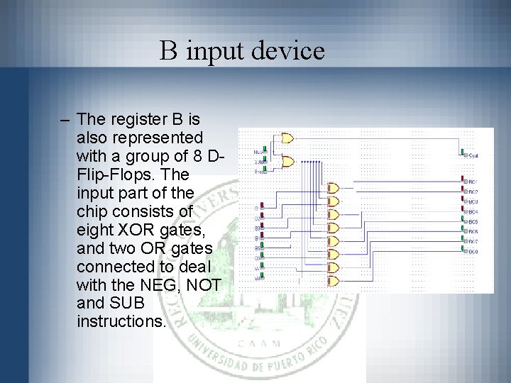
B input device – The register B is also represented with a group of 8 DFlip-Flops. The input part of the chip consists of eight XOR gates, and two OR gates connected to deal with the NEG, NOT and SUB instructions.

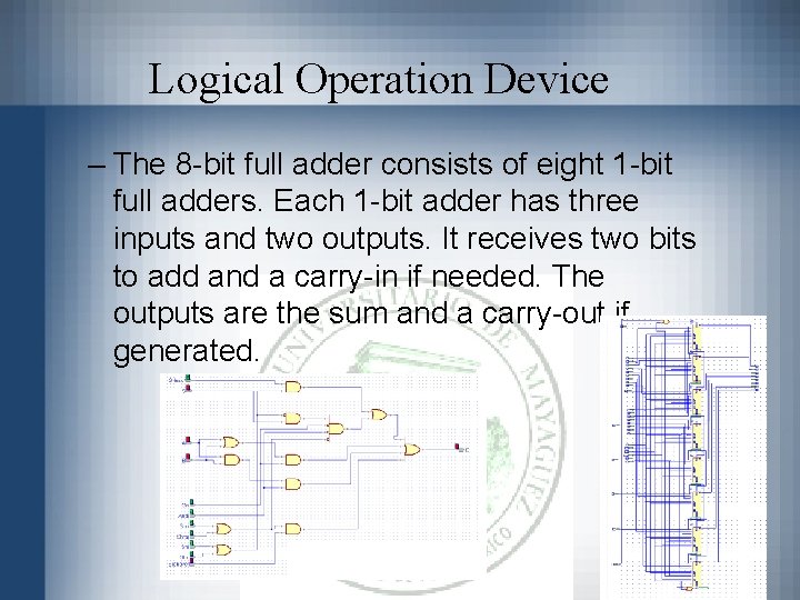
Logical Operation Device – The 8 -bit full adder consists of eight 1 -bit full adders. Each 1 -bit adder has three inputs and two outputs. It receives two bits to add and a carry-in if needed. The outputs are the sum and a carry-out if generated.

Sub-ALU

ALU

ALU

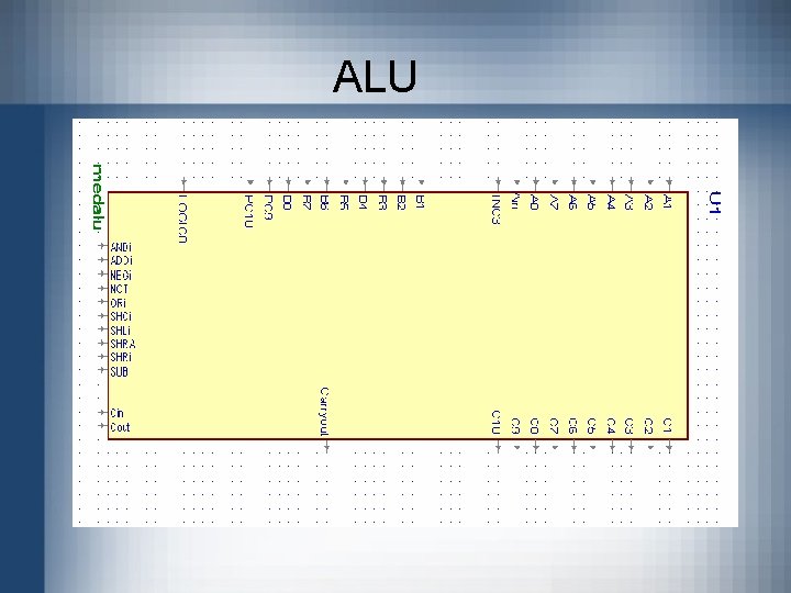
Conclusion The Arithmetic Logic Unit was implemented by doing a hardware design of the unit. The way the design was made is very easy to understand since it was made by doing block diagrams of the different parts of the device. This abstraction made us understand better each part of the unit and realize how important these parts are for the correct operation of the ALU. The bus that was utilized made it easier to understand the circuit even dough in the practical area this design will be much slower than designs using two or three buses. In conclusion this ALU device will work with the SRC architecture because it implements every instruction of the SRC.

Future Work There could be more projects based in the implementation of the Arithmetic Logic Unit. First the ALU can be improved in many ways by changing parts of the design or adding busses to the circuit. This can lead to create the entire Control Processing Unit of the SRC. Having done the CPU the entire processor can be done too.

References Computer Systems Design and Architecture Second Edition Vincent P. Heuring, Harry F. Jordan http: //ww. google. com http: //www. ece. uprm. edu/~nayda/Courses/arq/Projects/Proj 2/VHDL/

Acknowledgements • • • Chori’s Café Sociedad de los Buhos Prof. Nayda Santiago

¿Preguntas?