Lecture 17 Adders Outline q q q q
![Knowles [2, 1, 1, 1] 17: Adders CMOS VLSI Design 4 th Ed. 138 Knowles [2, 1, 1, 1] 17: Adders CMOS VLSI Design 4 th Ed. 138](https://slidetodoc.com/presentation_image_h/e5efdf22492bfd5d018944a98877a8b2/image-138.jpg)
- Slides: 160

Lecture 17: Adders

Outline q q q q q Datapath Computer Arithmetic Principles Single-bit Addition Carry-Ripple Adder Carry-Skip Adder Carry-Lookahead Adder Carry-Select Adder Carry-Increment Adder Tree Adder 17: Adders CMOS VLSI Design 4 th Ed. 2

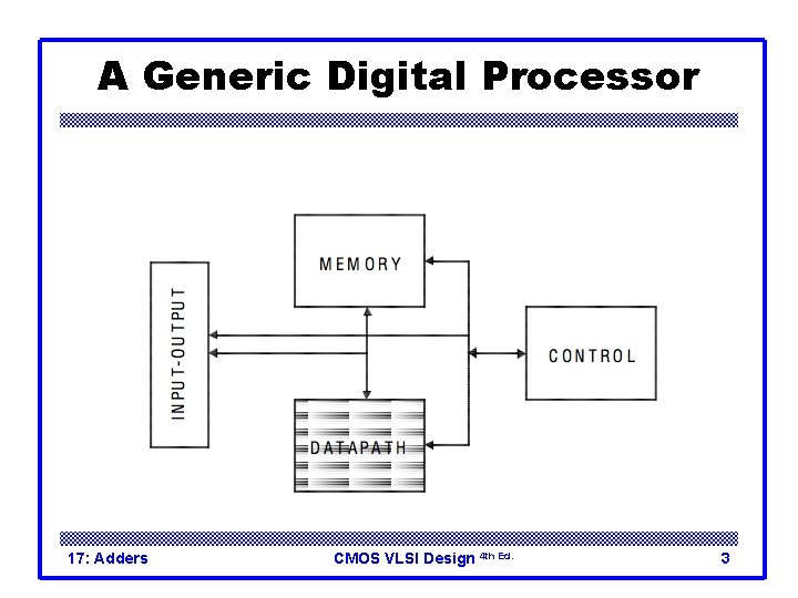
A Generic Digital Processor 17: Adders CMOS VLSI Design 4 th Ed. 3

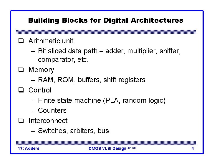
Building Blocks for Digital Architectures q Arithmetic unit – Bit sliced data path – adder, multiplier, shifter, comparator, etc. q Memory – RAM, ROM, buffers, shift registers q Control – Finite state machine (PLA, random logic) – Counters q Interconnect – Switches, arbiters, bus 17: Adders CMOS VLSI Design 4 th Ed. 4

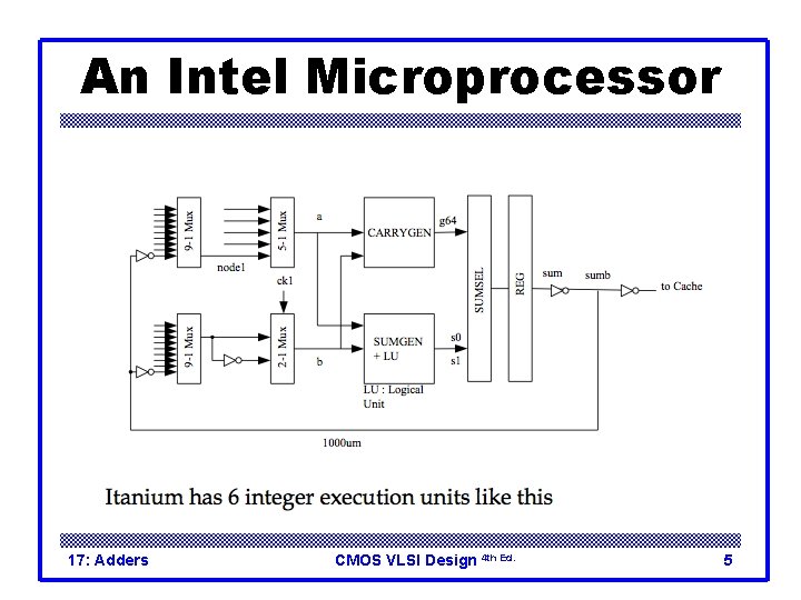
An Intel Microprocessor 17: Adders CMOS VLSI Design 4 th Ed. 5

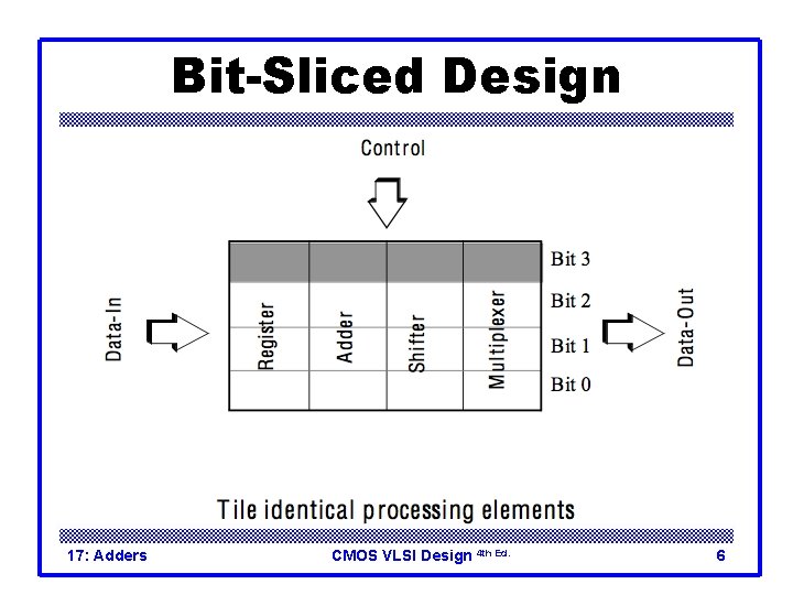
Bit-Sliced Design 17: Adders CMOS VLSI Design 4 th Ed. 6

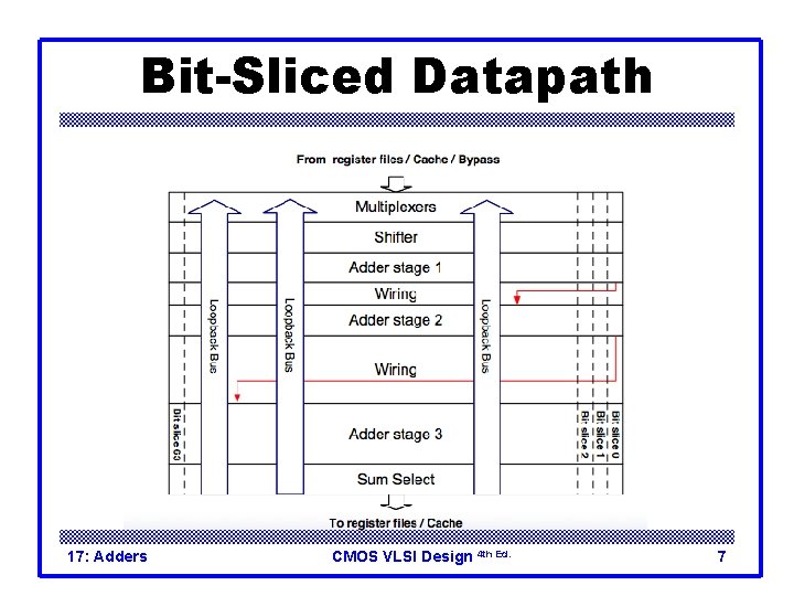
Bit-Sliced Datapath 17: Adders CMOS VLSI Design 4 th Ed. 7

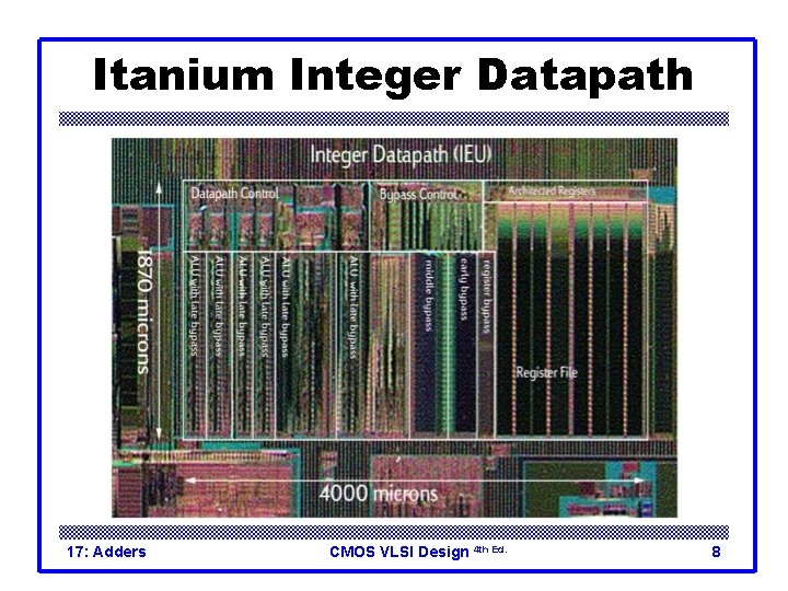
Itanium Integer Datapath 17: Adders CMOS VLSI Design 4 th Ed. 8

Motivation q Arithmetic units are, among others, core of every data path and addressing unit. q Data path is at the core of – microprocessors (CPU) – signal processors (DSP) – data processing application specific IC’s (ASIC) and programmable IC’s (FPGA) q Standard arithmetic units available from libraries q Design of arithmetic units necessary for – non-standard operations – high performance components – library development 17: Adders CMOS VLSI Design 4 th Ed. 9

Naming Conventions q Signal busses: A (1 -D), Ai, (2 -D), ai: k (sub-bus, 1 -D) q Signals: a, ai (1 -D), ai, k (2 -D), Ai: k (group signal) q Circuit complexity measures: A (Area), T (cycle time, delay), AT (area-time product), L (latency, number of cycles). q Arithmetic operators: +, -, • , /, log (=log 2) q Logic operators: OR, AND, XOR, NOT, … 17: Adders CMOS VLSI Design 4 th Ed. 10

Circuit Complexity Measures q Unit gate model – Inverter, buffer: A = 0, T = 0 – Simple monotonic 2 -input gates (AND, OR, NAND, NOR): A = 1, T = 1 – Simple non-monotonic 2 -input gates (XOR, XNOR): A = 2, T = 2 – Simple m-input gates: A = m – 1, T = – Wiring not considered – Only for estimation purposes 17: Adders CMOS VLSI Design 4 th Ed. 11

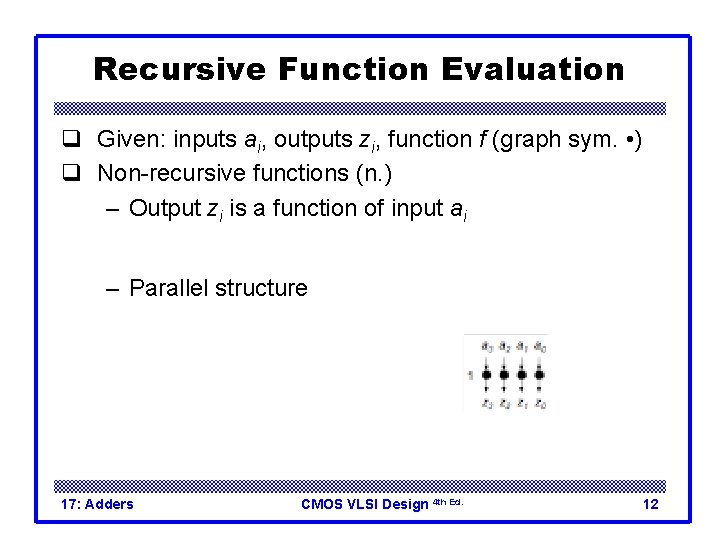
Recursive Function Evaluation q Given: inputs ai, outputs zi, function f (graph sym. • ) q Non-recursive functions (n. ) – Output zi is a function of input ai – Parallel structure 17: Adders CMOS VLSI Design 4 th Ed. 12

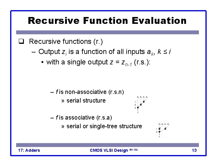
Recursive Function Evaluation q Recursive functions (r. ) – Output zi is a function of all inputs ak, k ≤ i • with a single output z = zn-1 (r. s. ): – f is non-associative (r. s. n) » serial structure – f is associative (r. s. a) » serial or single-tree structure 17: Adders CMOS VLSI Design 4 th Ed. 13

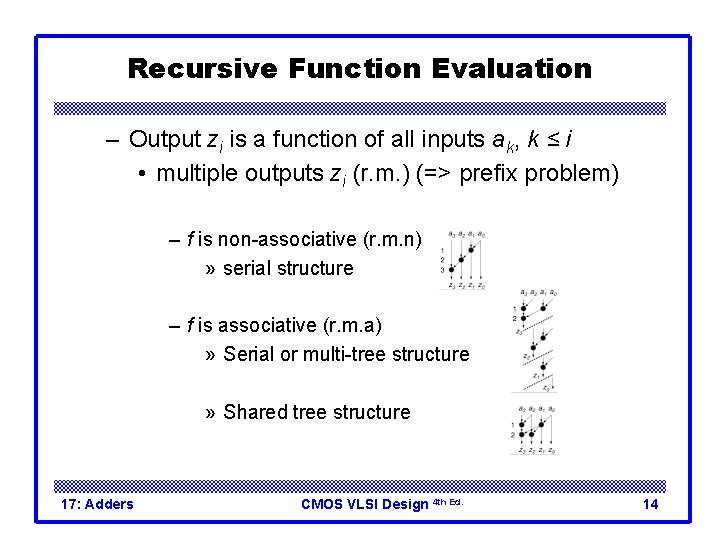
Recursive Function Evaluation – Output zi is a function of all inputs ak, k ≤ i • multiple outputs zi (r. m. ) (=> prefix problem) – f is non-associative (r. m. n) » serial structure – f is associative (r. m. a) » Serial or multi-tree structure » Shared tree structure 17: Adders CMOS VLSI Design 4 th Ed. 14

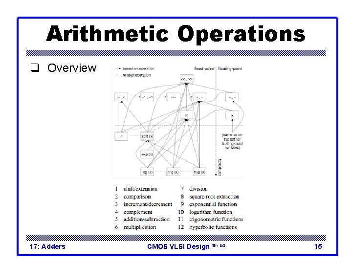
Arithmetic Operations q Overview 17: Adders CMOS VLSI Design 4 th Ed. 15

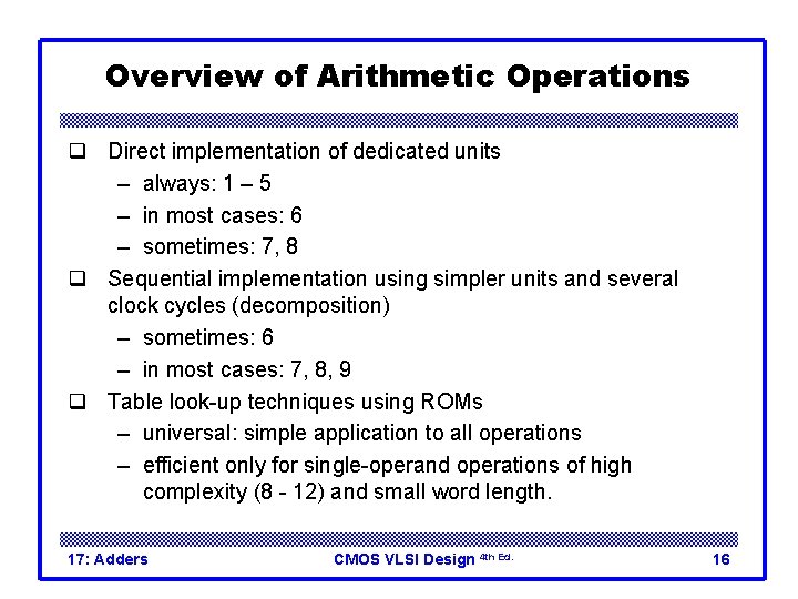
Overview of Arithmetic Operations q Direct implementation of dedicated units – always: 1 – 5 – in most cases: 6 – sometimes: 7, 8 q Sequential implementation using simpler units and several clock cycles (decomposition) – sometimes: 6 – in most cases: 7, 8, 9 q Table look-up techniques using ROMs – universal: simple application to all operations – efficient only for single-operand operations of high complexity (8 - 12) and small word length. 17: Adders CMOS VLSI Design 4 th Ed. 16

Overview of Arithmetic Operations q Approximation using simpler units: 7 – 12 – Taylor series expansion – polynomial and rational approximations – convergence of recursive equation systems – CORDIC (COordinate Rotation DIgital Computer) 17: Adders CMOS VLSI Design 4 th Ed. 17

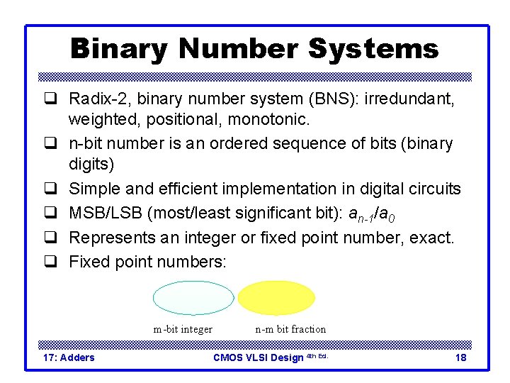
Binary Number Systems q Radix-2, binary number system (BNS): irredundant, weighted, positional, monotonic. q n-bit number is an ordered sequence of bits (binary digits) q Simple and efficient implementation in digital circuits q MSB/LSB (most/least significant bit): an-1/a 0 q Represents an integer or fixed point number, exact. q Fixed point numbers: m-bit integer 17: Adders n-m bit fraction CMOS VLSI Design 4 th Ed. 18

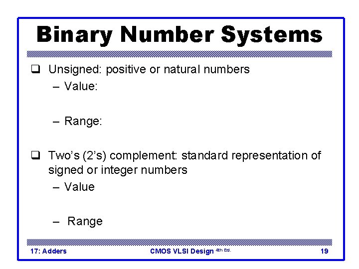
Binary Number Systems q Unsigned: positive or natural numbers – Value: – Range: q Two’s (2’s) complement: standard representation of signed or integer numbers – Value – Range 17: Adders CMOS VLSI Design 4 th Ed. 19

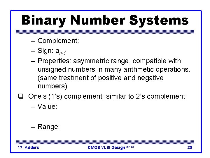
Binary Number Systems – Complement: – Sign: an-1 – Properties: asymmetric range, compatible with unsigned numbers in many arithmetic operations. (same treatment of positive and negative numbers) q One’s (1’s) complement: similar to 2’s complement – Value: – Range: 17: Adders CMOS VLSI Design 4 th Ed. 20

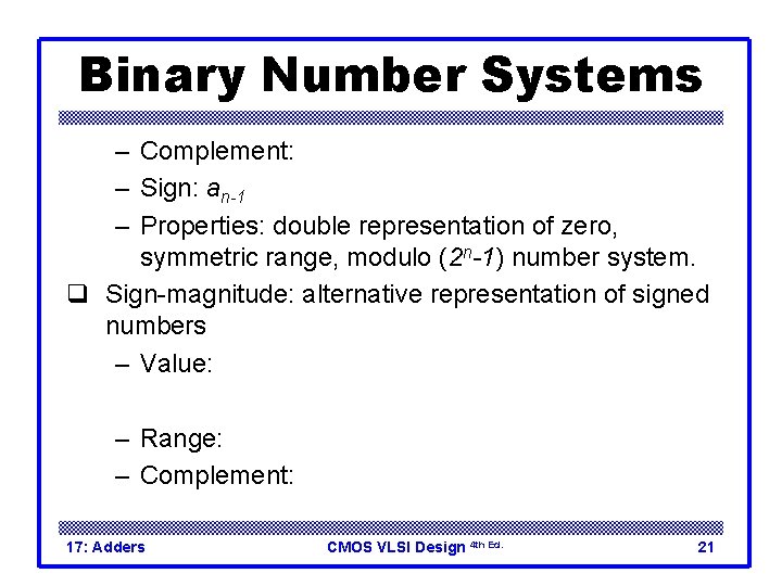
Binary Number Systems – Complement: – Sign: an-1 – Properties: double representation of zero, symmetric range, modulo (2 n-1) number system. q Sign-magnitude: alternative representation of signed numbers – Value: – Range: – Complement: 17: Adders CMOS VLSI Design 4 th Ed. 21

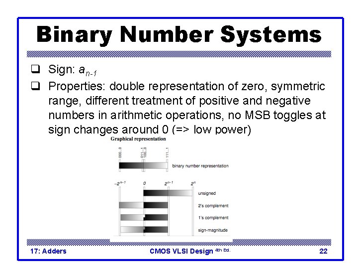
Binary Number Systems q Sign: an-1 q Properties: double representation of zero, symmetric range, different treatment of positive and negative numbers in arithmetic operations, no MSB toggles at sign changes around 0 (=> low power) 17: Adders CMOS VLSI Design 4 th Ed. 22

Gray Numbers q Gray numbers (code): binary, irredundant, nonweighted, non-monotonic. – Property: unit-distance coding. Exactly one-bit toggles between adjacent numbers. – Applications: counters with low output toggle rate (low power busses), representation of continuous signals for low-error sampling (no false numbers due to switching of different bits at different times). – Non-monotonic numbers: difficult arithmetic operations (addition, comparison). 17: Adders CMOS VLSI Design 4 th Ed. 23

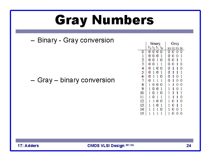
Gray Numbers – Binary - Gray conversion – Gray – binary conversion 17: Adders CMOS VLSI Design 4 th Ed. 24

Redundant Number Systems q Non-binary, redundant, weighted number systems. q Digit set larger than radix (typically radix 2) => multiple representations of the same number => redundancy. q No carry propagation in adders => more efficient implementation of adder-based units (multipliers, dividers, etc. ) q Redundancy => no direct implementation of relational operators => conversion to irredundant numbers. q Several bits used to represent one digit => higher storage requirements. q Expensive conversion to irredundant numbers. Not necessary if redundant input operators are allowed. 17: Adders CMOS VLSI Design 4 th Ed. 25

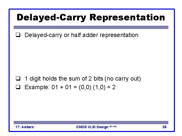
Delayed-Carry Representation q Delayed-carry or half adder representation q 1 digit holds the sum of 2 bits (no carry out) q Example: 01 + 01 = (0, 0) (1, 0) = 2 17: Adders CMOS VLSI Design 4 th Ed. 26

Carry-Save Representation q One digit holds the sum of 3 bits or 1 digit and 1 bit. No carry-out digit, carry is saved. q Standard redundant number system for fast addition. 17: Adders CMOS VLSI Design 4 th Ed. 27

Signed-Digit Representation q Signed-digit (SD) or redundant digit (RD) number representation. q No carry propagation in S = R + T q One digit holds the sum of two digits. No carry-out. 17: Adders CMOS VLSI Design 4 th Ed. 28

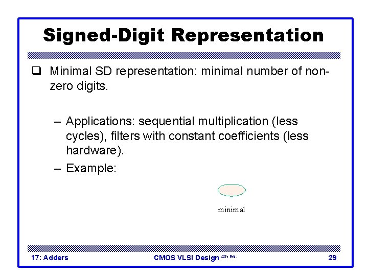
Signed-Digit Representation q Minimal SD representation: minimal number of nonzero digits. – Applications: sequential multiplication (less cycles), filters with constant coefficients (less hardware). – Example: minimal 17: Adders CMOS VLSI Design 4 th Ed. 29

Signed-Digit Representation q Canonical SD representation: minimal SD. Not two non-zero digits in sequence. q SD -> binary: carry propagation necessary => adder. q Other applications: high speed multipliers. q Similar to carry-save, simple use for signed numbers. 17: Adders CMOS VLSI Design 4 th Ed. 30

Residue Number Systems q Non-binary, irredundant, non-weighted number system. q Carry-free and fast additions and multiplications. q Complex and slow other arithmetic operations (e. g. comparison, sign, and overflow detection) because digits are not weighted. Conversion to weighted mixed-radix or binary system required. q Codes for error correction and detection. q Possible applications (but hardly used) – Digital filters – Error detection and correction 17: Adders CMOS VLSI Design 4 th Ed. 31

Residue Number Systems q Base is n-tuple of integers (mn-1, mn-2, …, m 0), residues (or moduli). These mi are pairwise prime. q Arithmetic operations: each digit computed separately. 17: Adders CMOS VLSI Design 4 th Ed. 32

Residue Number Systems q Best moduli mi are 2 k and 2 k – 1. – High storage efficiency with k bits. – Simple modular addition k bit adder without cout 17: Adders CMOS VLSI Design 4 th Ed. 33

Residue Number Systems q Example: 17: Adders CMOS VLSI Design 4 th Ed. 34

Floating-Point Numbers q Larger range, smaller precision than fixed-point representation, inexact, real numbers. q Double-number form => discontinuous precision. q S | biased exponent E | unsigned norm mantissa M q Basic arithmetic operations 17: Adders CMOS VLSI Design 4 th Ed. 35

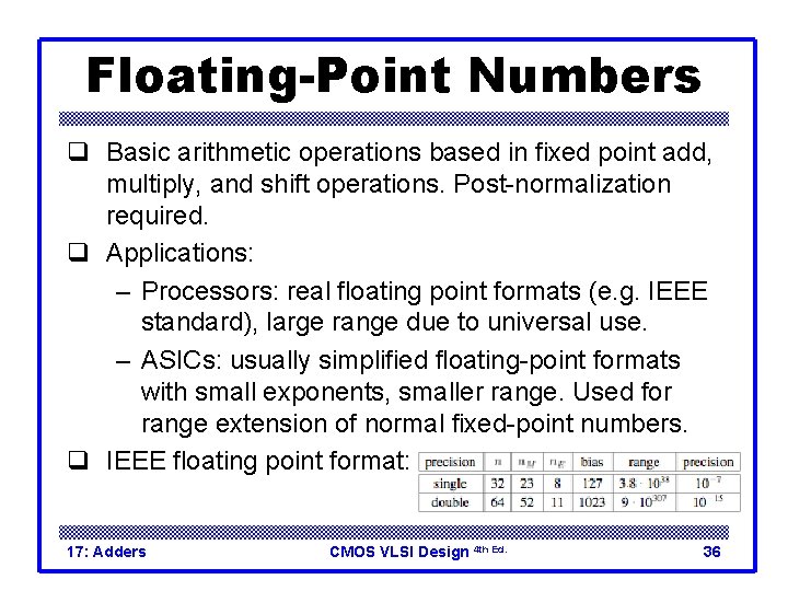
Floating-Point Numbers q Basic arithmetic operations based in fixed point add, multiply, and shift operations. Post-normalization required. q Applications: – Processors: real floating point formats (e. g. IEEE standard), large range due to universal use. – ASICs: usually simplified floating-point formats with small exponents, smaller range. Used for range extension of normal fixed-point numbers. q IEEE floating point format: 17: Adders CMOS VLSI Design 4 th Ed. 36

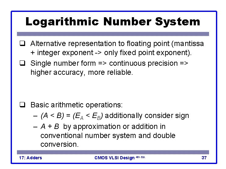
Logarithmic Number System q Alternative representation to floating point (mantissa + integer exponent -> only fixed point exponent). q Single number form => continuous precision => higher accuracy, more reliable. q Basic arithmetic operations: – (A < B) = (EA < EB) additionally consider sign – A + B by approximation or addition in conventional number system and double conversion. 17: Adders CMOS VLSI Design 4 th Ed. 37

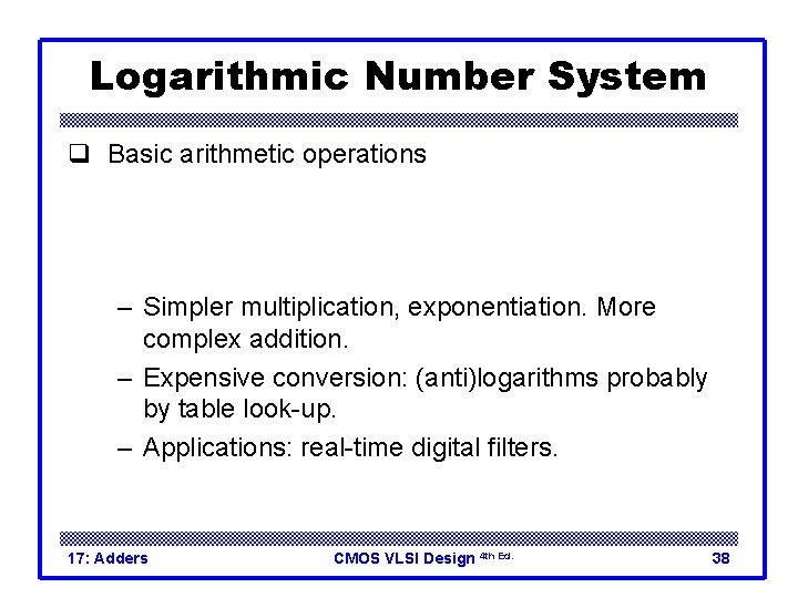
Logarithmic Number System q Basic arithmetic operations – Simpler multiplication, exponentiation. More complex addition. – Expensive conversion: (anti)logarithms probably by table look-up. – Applications: real-time digital filters. 17: Adders CMOS VLSI Design 4 th Ed. 38

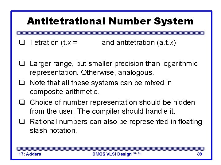
Antitetrational Number System q Tetration (t. x = and antitetration (a. t. x) q Larger range, but smaller precision than logarithmic representation. Otherwise, analogous. q Note that all these systems can be mixed in composite arithmetic. q Choice of number representation should be hidden from the user. The compiler should handle it. q Rational numbers can also be represented in floating slash notation. 17: Adders CMOS VLSI Design 4 th Ed. 39

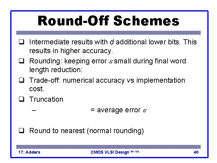
Round-Off Schemes q Intermediate results with d additional lower bits. This results in higher accuracy. q Rounding: keeping error e small during final word length reduction: q Trade-off: numerical accuracy vs implementation cost. q Truncation – = average error e q Round to nearest (normal rounding) 17: Adders CMOS VLSI Design 4 th Ed. 40

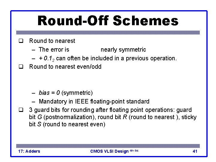
Round-Off Schemes q Round to nearest – The error is nearly symmetric – + 0. 12 can often be included in a previous operation. q Round to nearest even/odd – bias = 0 (symmetric) – Mandatory in IEEE floating-point standard q 3 guard bits for rounding after floating point operations: guard bit G (postnormalization), round bit R (round to nearest ), sticky bit S (round to nearest even) 17: Adders CMOS VLSI Design 4 th Ed. 41

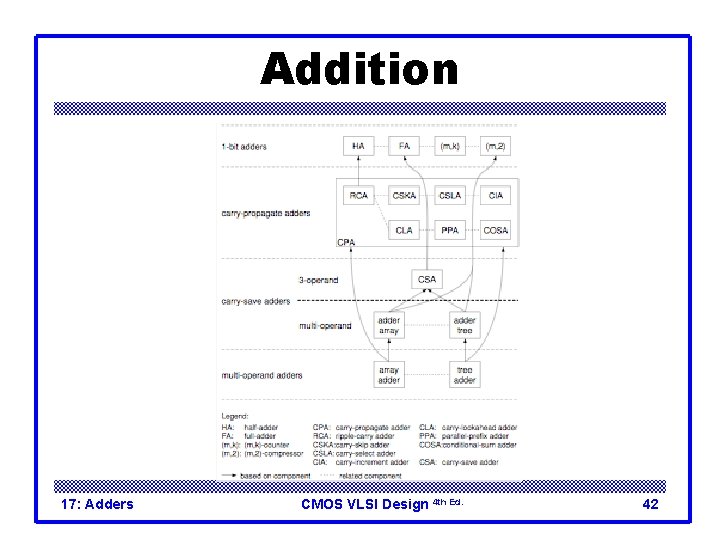
Addition 17: Adders CMOS VLSI Design 4 th Ed. 42

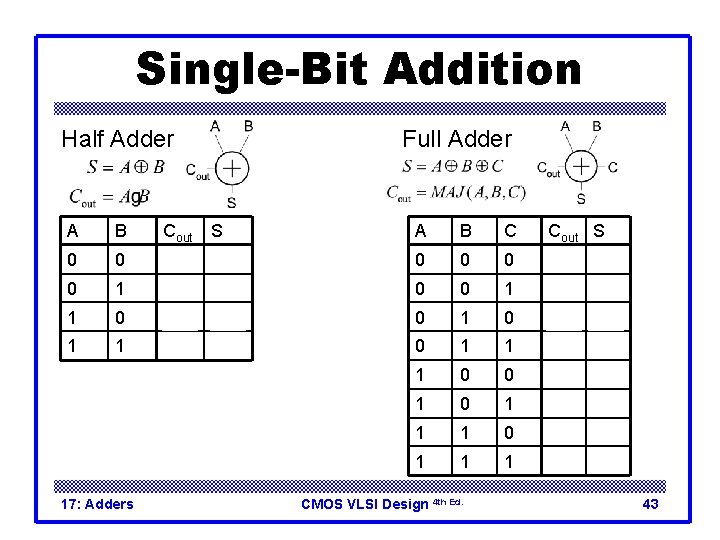
Single-Bit Addition Half Adder Full Adder A B Cout S A B C Cout S 0 0 0 0 0 1 0 0 1 1 0 0 1 1 1 0 0 0 1 1 0 1 1 17: Adders CMOS VLSI Design 4 th Ed. 43

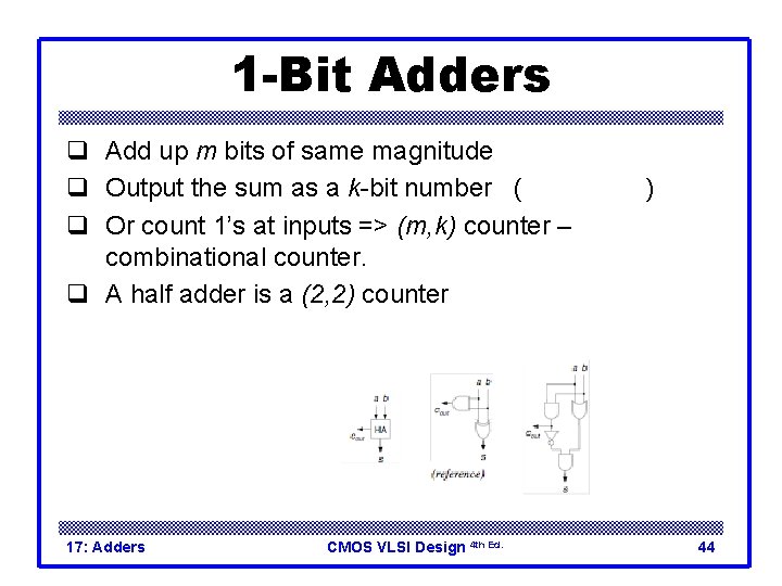
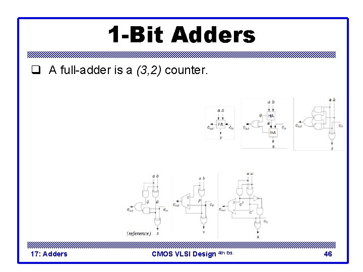
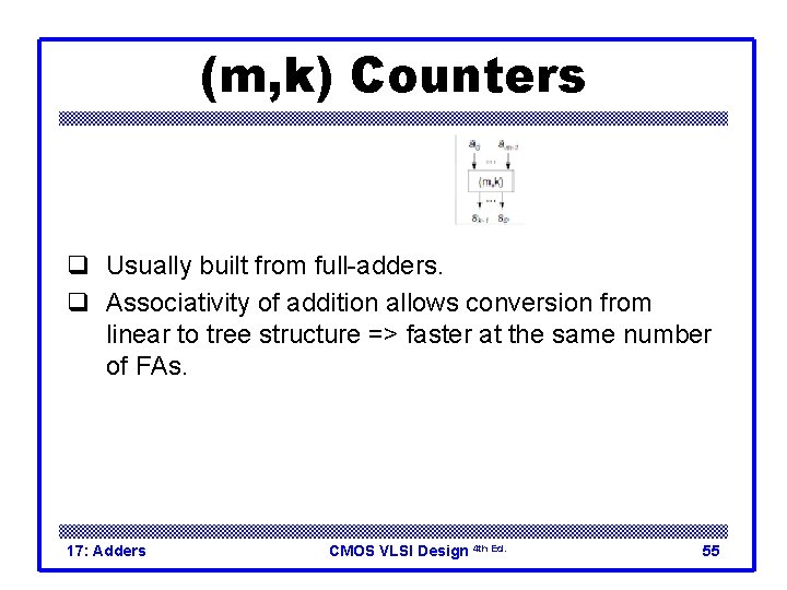
1 -Bit Adders q Add up m bits of same magnitude q Output the sum as a k-bit number ( q Or count 1’s at inputs => (m, k) counter – combinational counter. q A half adder is a (2, 2) counter 17: Adders CMOS VLSI Design 4 th Ed. ) 44

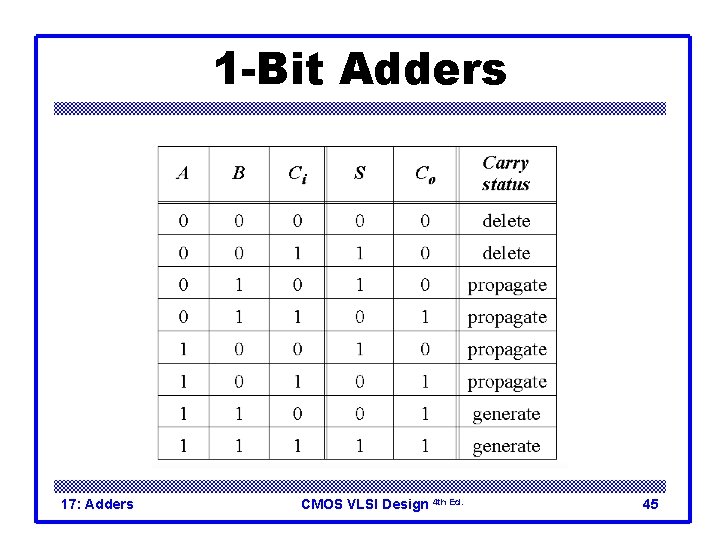
1 -Bit Adders 17: Adders CMOS VLSI Design 4 th Ed. 45

1 -Bit Adders q A full-adder is a (3, 2) counter. 17: Adders CMOS VLSI Design 4 th Ed. 46

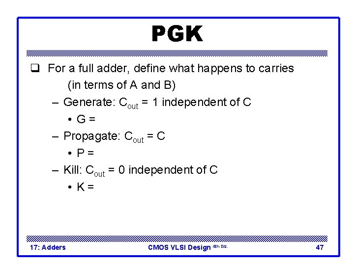
PGK q For a full adder, define what happens to carries (in terms of A and B) – Generate: Cout = 1 independent of C • G=A • B – Propagate: Cout = C • P=A B – Kill: Cout = 0 independent of C • K = ~A • ~B 17: Adders CMOS VLSI Design 4 th Ed. 47

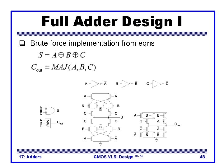
Full Adder Design I q Brute force implementation from eqns 17: Adders CMOS VLSI Design 4 th Ed. 48

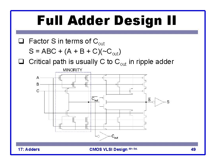
Full Adder Design II q Factor S in terms of Cout S = ABC + (A + B + C)(~Cout) q Critical path is usually C to Cout in ripple adder 17: Adders CMOS VLSI Design 4 th Ed. 49

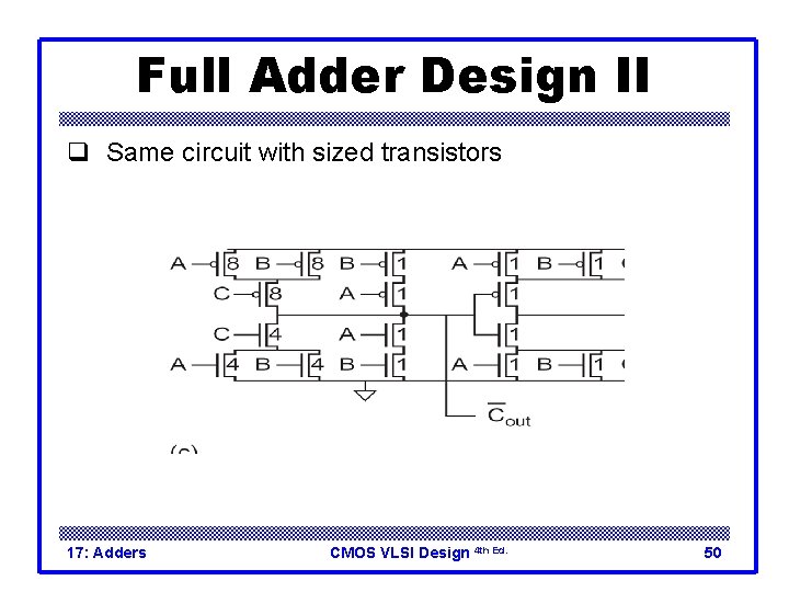
Full Adder Design II q Same circuit with sized transistors 17: Adders CMOS VLSI Design 4 th Ed. 50

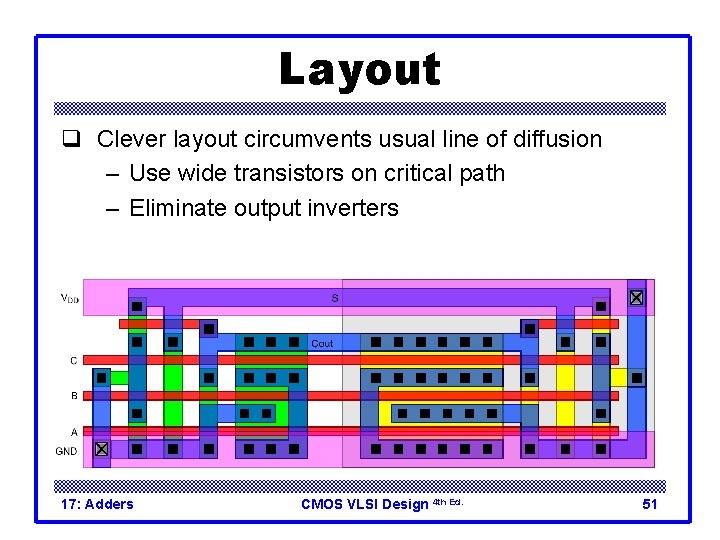
Layout q Clever layout circumvents usual line of diffusion – Use wide transistors on critical path – Eliminate output inverters 17: Adders CMOS VLSI Design 4 th Ed. 51

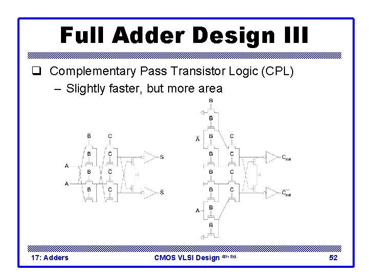
Full Adder Design III q Complementary Pass Transistor Logic (CPL) – Slightly faster, but more area 17: Adders CMOS VLSI Design 4 th Ed. 52

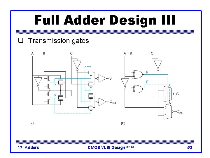
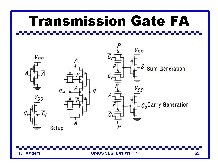
Full Adder Design III q Transmission gates 17: Adders CMOS VLSI Design 4 th Ed. 53

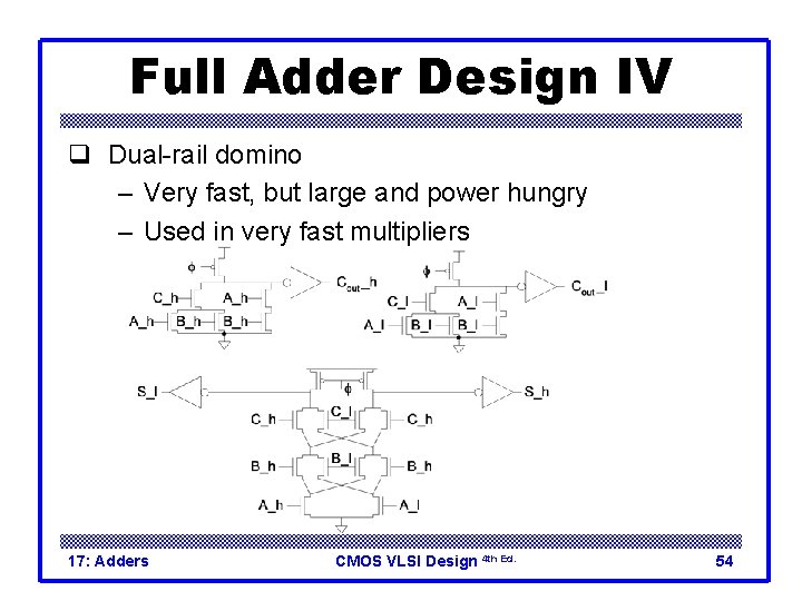
Full Adder Design IV q Dual-rail domino – Very fast, but large and power hungry – Used in very fast multipliers 17: Adders CMOS VLSI Design 4 th Ed. 54

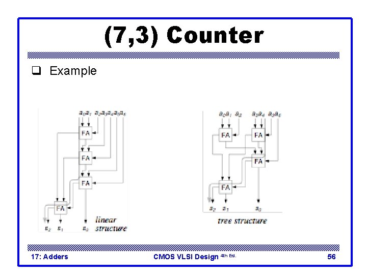
(m, k) Counters q Usually built from full-adders. q Associativity of addition allows conversion from linear to tree structure => faster at the same number of FAs. 17: Adders CMOS VLSI Design 4 th Ed. 55

(7, 3) Counter q Example 17: Adders CMOS VLSI Design 4 th Ed. 56

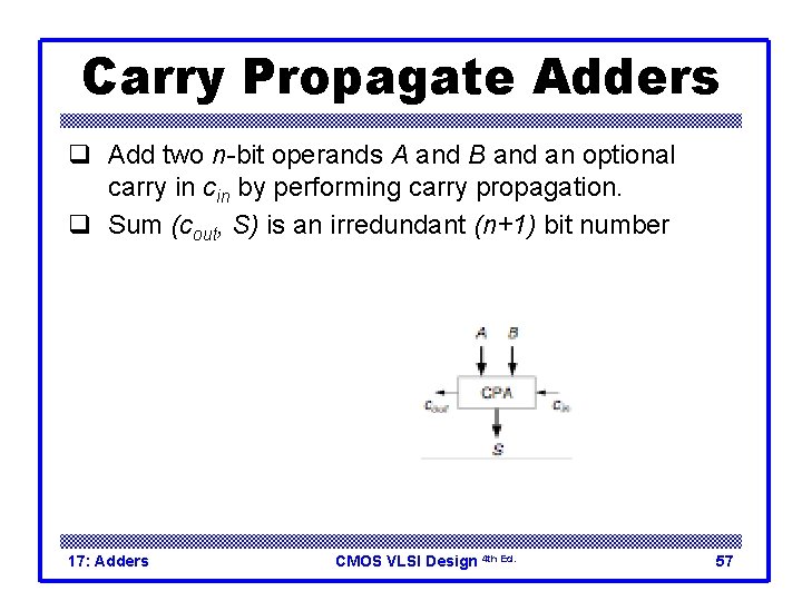
Carry Propagate Adders q Add two n-bit operands A and B and an optional carry in cin by performing carry propagation. q Sum (cout, S) is an irredundant (n+1) bit number 17: Adders CMOS VLSI Design 4 th Ed. 57

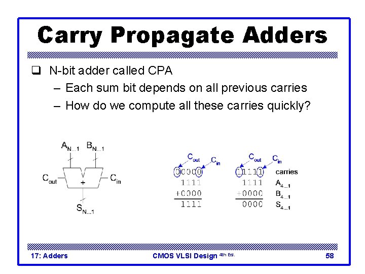
Carry Propagate Adders q N-bit adder called CPA – Each sum bit depends on all previous carries – How do we compute all these carries quickly? 17: Adders CMOS VLSI Design 4 th Ed. 58

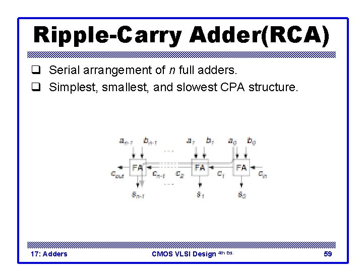
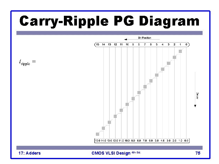
Ripple-Carry Adder(RCA) q Serial arrangement of n full adders. q Simplest, smallest, and slowest CPA structure. 17: Adders CMOS VLSI Design 4 th Ed. 59

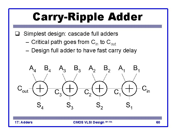
Carry-Ripple Adder q Simplest design: cascade full adders – Critical path goes from Cin to Cout – Design full adder to have fast carry delay 17: Adders CMOS VLSI Design 4 th Ed. 60

Carry Ripple Adder q Note that worst case delay is linear with number of bits. q Goal: Make the fastest possible carry path circuit. 17: Adders CMOS VLSI Design 4 th Ed. 61

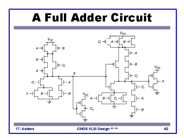
A Full Adder Circuit 17: Adders CMOS VLSI Design 4 th Ed. 62

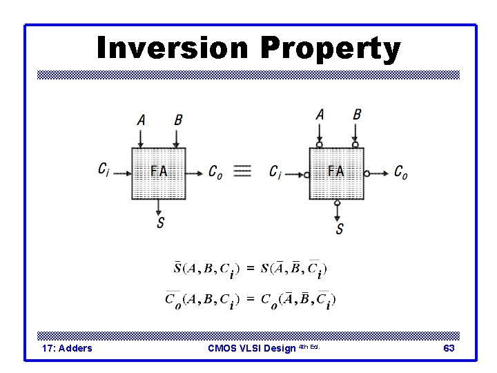
Inversion Property 17: Adders CMOS VLSI Design 4 th Ed. 63

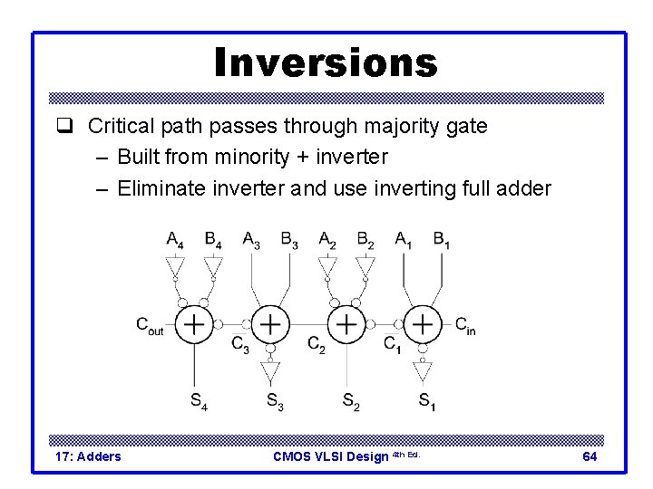
Inversions q Critical path passes through majority gate – Built from minority + inverter – Eliminate inverter and use inverting full adder 17: Adders CMOS VLSI Design 4 th Ed. 64

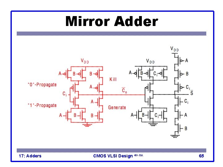
Mirror Adder 17: Adders CMOS VLSI Design 4 th Ed. 65

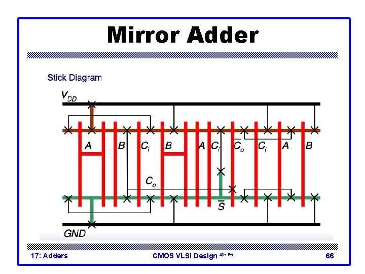
Mirror Adder 17: Adders CMOS VLSI Design 4 th Ed. 66

Mirror Adder q The NMOS and PMOS chains are completely symmetrical. A maximum of two series transistors can be observed in the carry generation circuit. q When laying out the cell, the most critical issue is the minimization of the capacitance at node Co. The reduction of the diffusion capacitances is particularly important. q The capacitance at node Co is composed of four diffusion capacitances, two internal gate capacitances, and six gate capacitances in the connecting adder cell. 17: Adders CMOS VLSI Design 4 th Ed. 67

Mirror Adder q The transistors connected to Ci are placed closest to the input. q Only the transistors in the carry stage have to be optimized for optimal speed. All transistors in the sum stage can be minimal size. 17: Adders CMOS VLSI Design 4 th Ed. 68

Transmission Gate FA 17: Adders CMOS VLSI Design 4 th Ed. 69

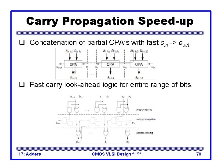
Carry Propagation Speed-up q Concatenation of partial CPA’s with fast cin -> cout. q Fast carry look-ahead logic for entire range of bits. 17: Adders CMOS VLSI Design 4 th Ed. 70

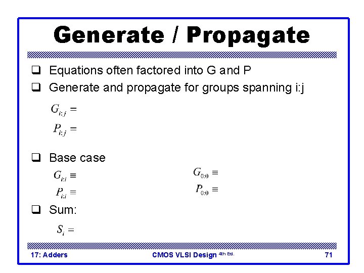
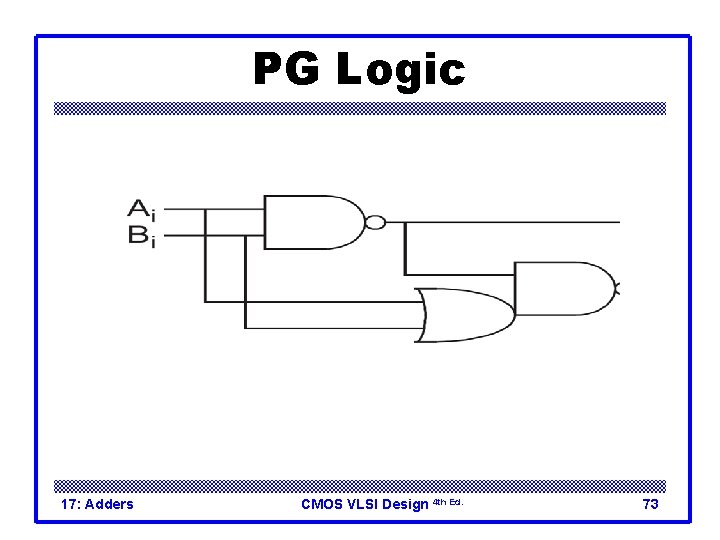
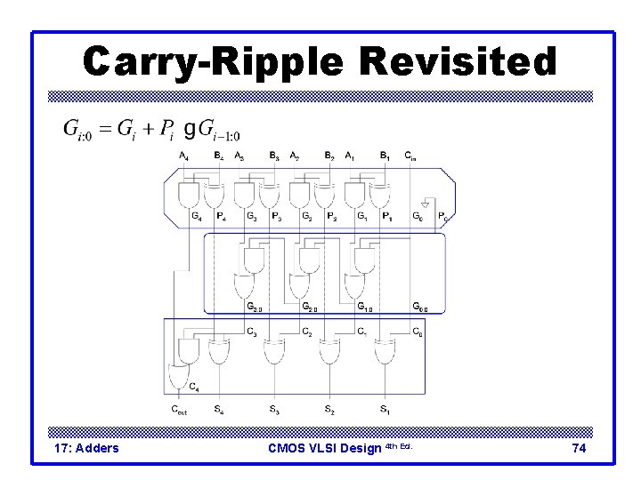
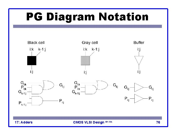
Generate / Propagate q Equations often factored into G and P q Generate and propagate for groups spanning i: j q Base case q Sum: 17: Adders CMOS VLSI Design 4 th Ed. 71

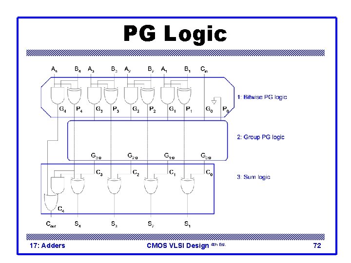
PG Logic 17: Adders CMOS VLSI Design 4 th Ed. 72

PG Logic 17: Adders CMOS VLSI Design 4 th Ed. 73

Carry-Ripple Revisited 17: Adders CMOS VLSI Design 4 th Ed. 74

Carry-Ripple PG Diagram 17: Adders CMOS VLSI Design 4 th Ed. 75

PG Diagram Notation 17: Adders CMOS VLSI Design 4 th Ed. 76

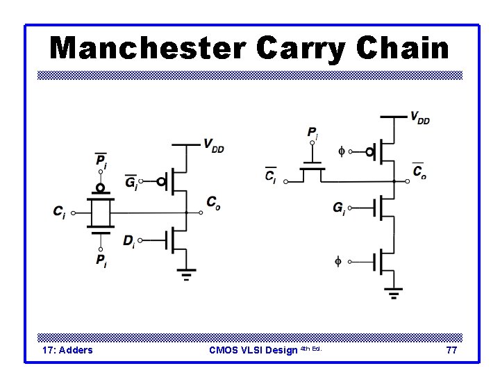
Manchester Carry Chain 17: Adders CMOS VLSI Design 4 th Ed. 77

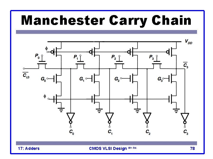
Manchester Carry Chain 17: Adders CMOS VLSI Design 4 th Ed. 78

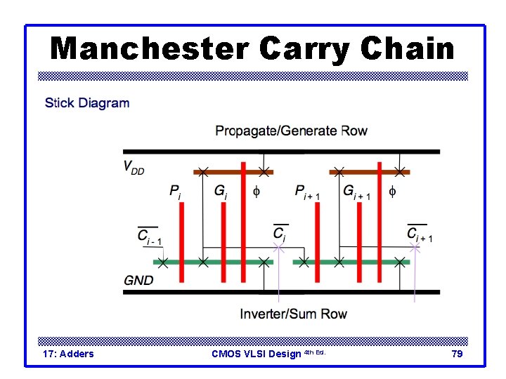
Manchester Carry Chain 17: Adders CMOS VLSI Design 4 th Ed. 79

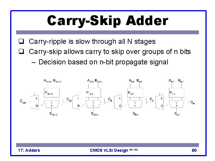
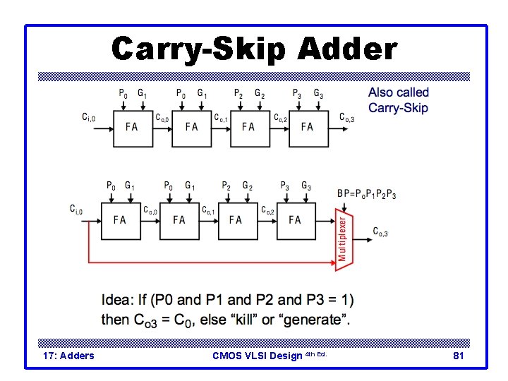
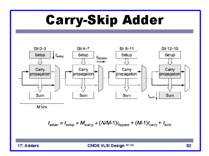
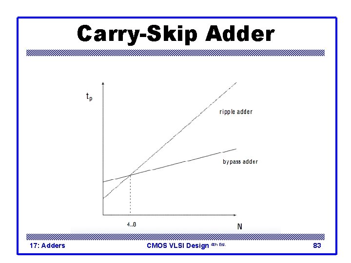
Carry-Skip Adder q Carry-ripple is slow through all N stages q Carry-skip allows carry to skip over groups of n bits – Decision based on n-bit propagate signal 17: Adders CMOS VLSI Design 4 th Ed. 80

Carry-Skip Adder 17: Adders CMOS VLSI Design 4 th Ed. 81

Carry-Skip Adder 17: Adders CMOS VLSI Design 4 th Ed. 82

Carry-Skip Adder 17: Adders CMOS VLSI Design 4 th Ed. 83

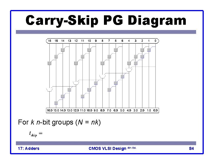
Carry-Skip PG Diagram For k n-bit groups (N = nk) 17: Adders CMOS VLSI Design 4 th Ed. 84

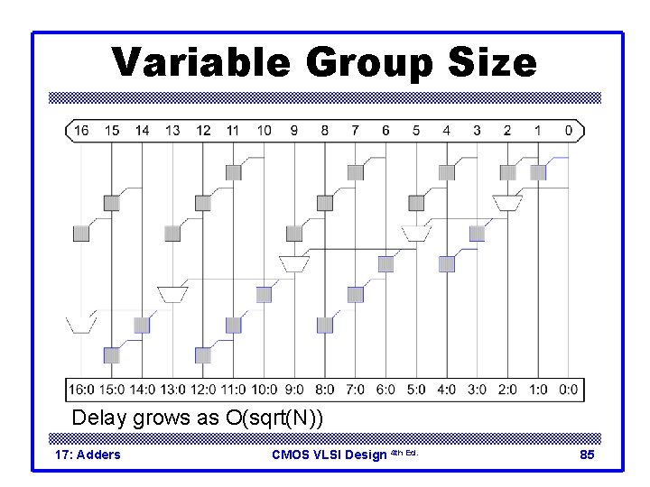
Variable Group Size Delay grows as O(sqrt(N)) 17: Adders CMOS VLSI Design 4 th Ed. 85

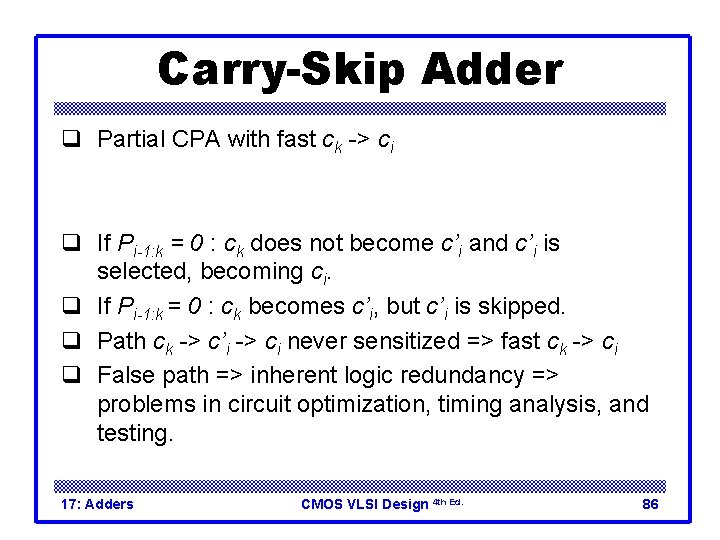
Carry-Skip Adder q Partial CPA with fast ck -> ci q If Pi-1: k = 0 : ck does not become c’i and c’i is selected, becoming ci. q If Pi-1: k = 0 : ck becomes c’i, but c’i is skipped. q Path ck -> c’i -> ci never sensitized => fast ck -> ci q False path => inherent logic redundancy => problems in circuit optimization, timing analysis, and testing. 17: Adders CMOS VLSI Design 4 th Ed. 86

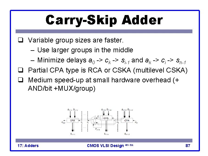
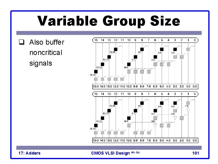
Carry-Skip Adder q Variable group sizes are faster. – Use larger groups in the middle – Minimize delays a 0 -> ck -> si-1 and ak -> ci -> sn-1 q Partial CPA type is RCA or CSKA (multilevel CSKA) q Medium speed-up at small hardware overhead (+ AND/bit +MUX/group) 17: Adders CMOS VLSI Design 4 th Ed. 87

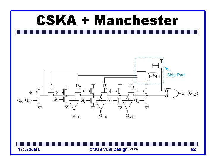
CSKA + Manchester 17: Adders CMOS VLSI Design 4 th Ed. 88

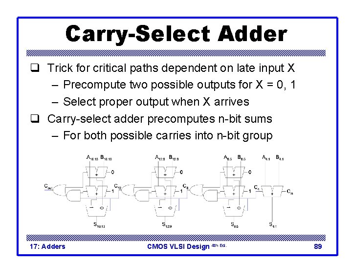
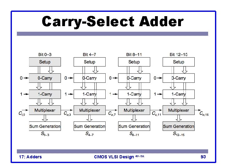
Carry-Select Adder q Trick for critical paths dependent on late input X – Precompute two possible outputs for X = 0, 1 – Select proper output when X arrives q Carry-select adder precomputes n-bit sums – For both possible carries into n-bit group 17: Adders CMOS VLSI Design 4 th Ed. 89

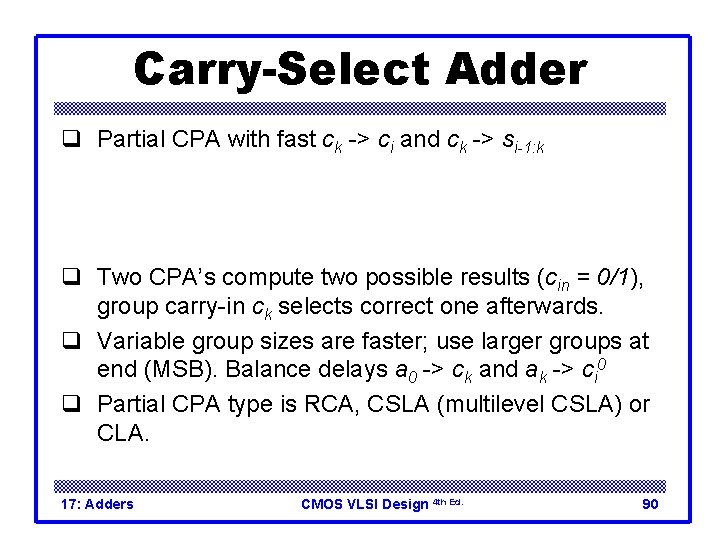
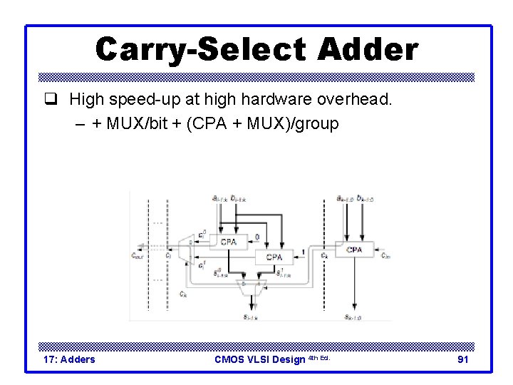
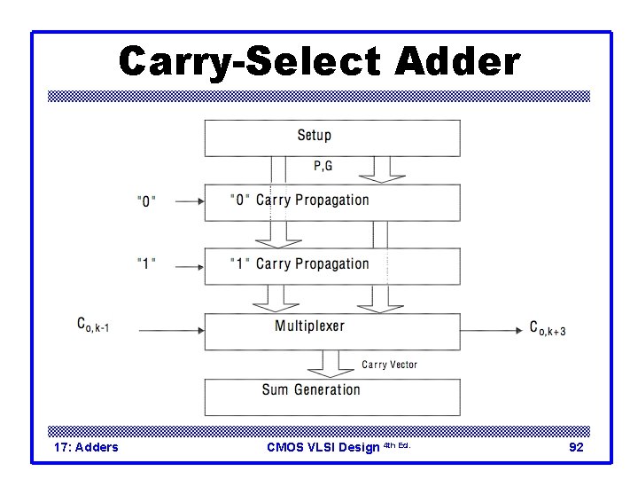
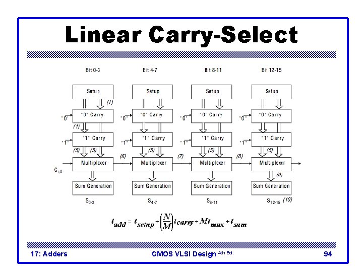
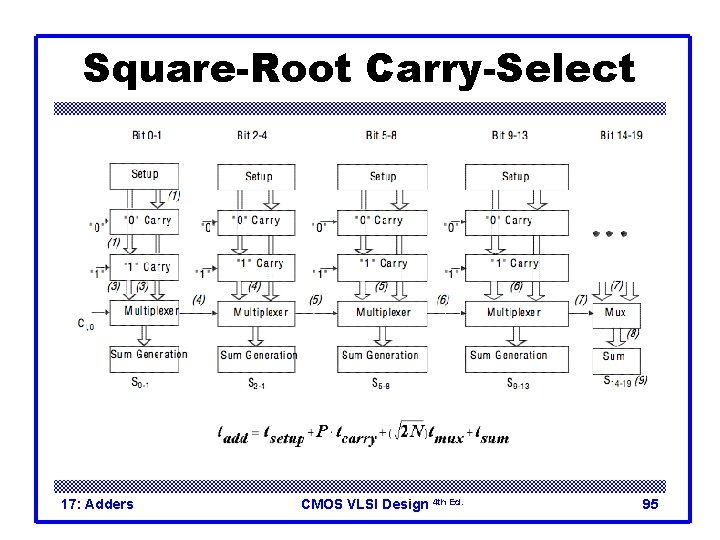
Carry-Select Adder q Partial CPA with fast ck -> ci and ck -> si-1: k q Two CPA’s compute two possible results (cin = 0/1), group carry-in ck selects correct one afterwards. q Variable group sizes are faster; use larger groups at end (MSB). Balance delays a 0 -> ck and ak -> ci 0 q Partial CPA type is RCA, CSLA (multilevel CSLA) or CLA. 17: Adders CMOS VLSI Design 4 th Ed. 90

Carry-Select Adder q High speed-up at high hardware overhead. – + MUX/bit + (CPA + MUX)/group 17: Adders CMOS VLSI Design 4 th Ed. 91

Carry-Select Adder 17: Adders CMOS VLSI Design 4 th Ed. 92

Carry-Select Adder 17: Adders CMOS VLSI Design 4 th Ed. 93

Linear Carry-Select 17: Adders CMOS VLSI Design 4 th Ed. 94

Square-Root Carry-Select 17: Adders CMOS VLSI Design 4 th Ed. 95

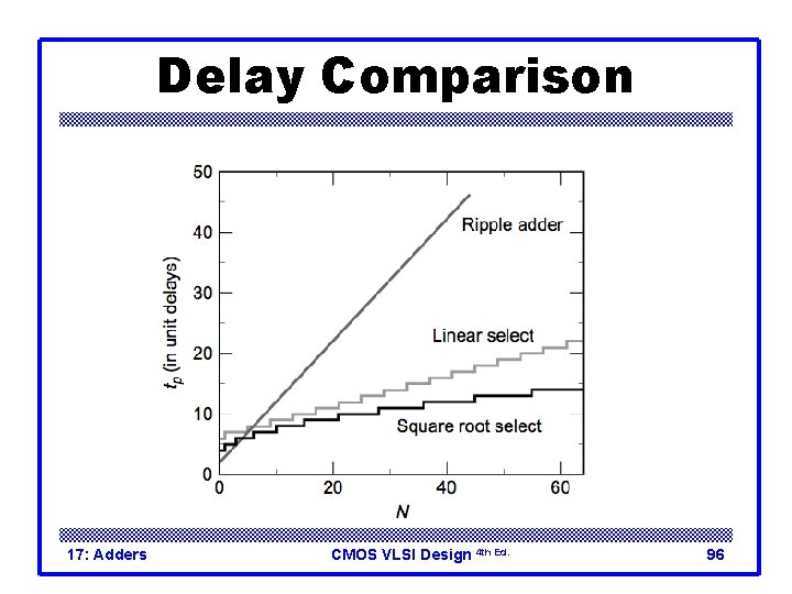
Delay Comparison 17: Adders CMOS VLSI Design 4 th Ed. 96

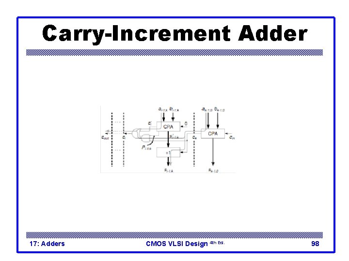
Carry-Increment Adder q Partial CPA with fast ck -> ci and ck -> si-1: k q Result is incremented after addition if ck = 1 q Variable group sizes are faster, use larger groups at end (MSB). Balance delays a 0 -> ck and ak -> c’i q Partial CPA could be RCA, CIA (multilevel CIA) or CLA. q High speed-up at medium hardware overhead (+AND/bit + (incrementer + AND/OR)/group). q Logic of CPA and incrementer could be merged. 17: Adders CMOS VLSI Design 4 th Ed. 97

Carry-Increment Adder 17: Adders CMOS VLSI Design 4 th Ed. 98

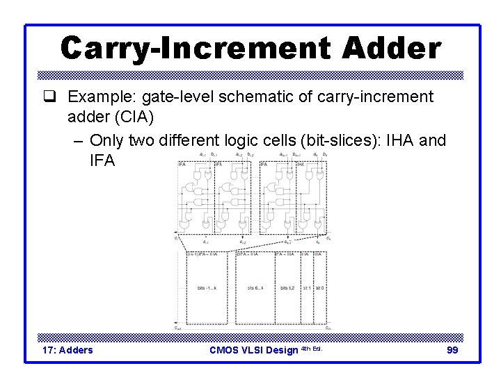
Carry-Increment Adder q Example: gate-level schematic of carry-increment adder (CIA) – Only two different logic cells (bit-slices): IHA and IFA 17: Adders CMOS VLSI Design 4 th Ed. 99

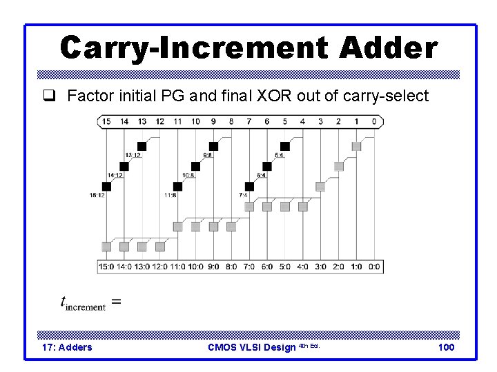
Carry-Increment Adder q Factor initial PG and final XOR out of carry-select 17: Adders CMOS VLSI Design 4 th Ed. 100

Variable Group Size q Also buffer noncritical signals 17: Adders CMOS VLSI Design 4 th Ed. 101

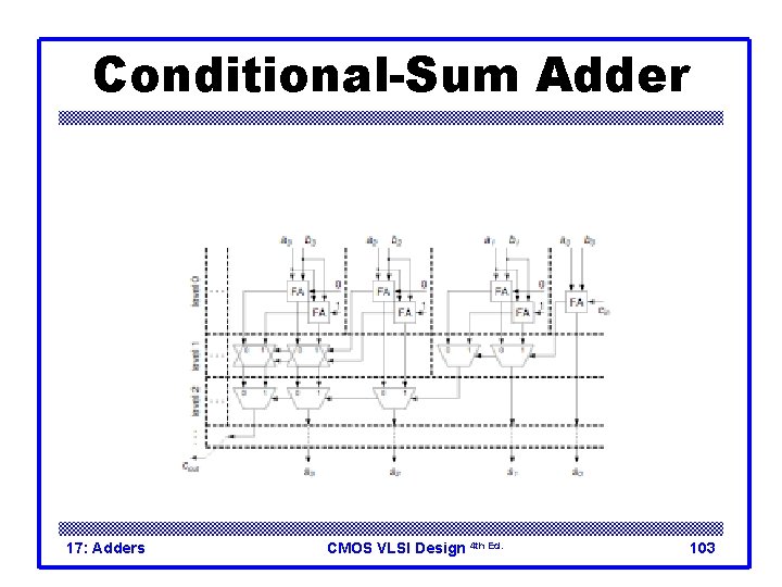
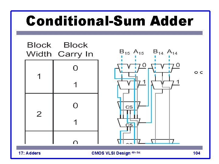
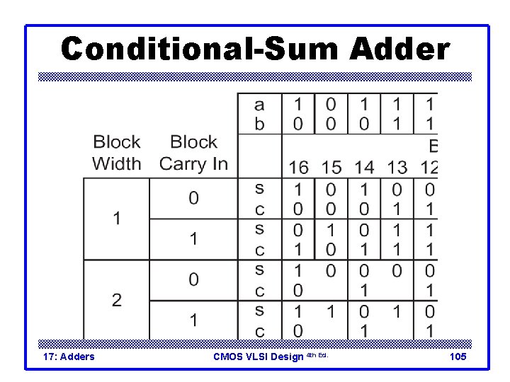
Conditional-Sum Adder q Optimized multilevel CSLA with logn levels q Correct sum bits or are conditionally selected through logn levels of multiplexers. q Bit groups of size 2 l at level l. q Higher parallelism, more balanced signal paths. q Highest speed-up at highest hardware overhead (2 RCA + more than logn MUX/bit) 17: Adders CMOS VLSI Design 4 th Ed. 102

Conditional-Sum Adder 17: Adders CMOS VLSI Design 4 th Ed. 103

Conditional-Sum Adder 17: Adders CMOS VLSI Design 4 th Ed. 104

Conditional-Sum Adder 17: Adders CMOS VLSI Design 4 th Ed. 105

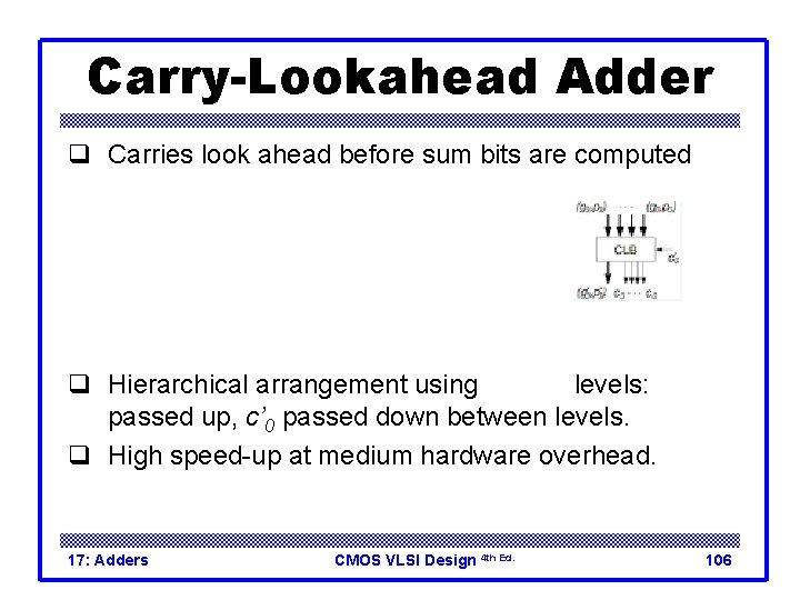
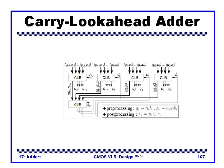
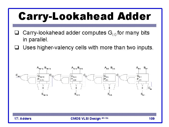
Carry-Lookahead Adder q Carries look ahead before sum bits are computed q Hierarchical arrangement using levels: passed up, c’ 0 passed down between levels. q High speed-up at medium hardware overhead. 17: Adders CMOS VLSI Design 4 th Ed. 106

Carry-Lookahead Adder 17: Adders CMOS VLSI Design 4 th Ed. 107

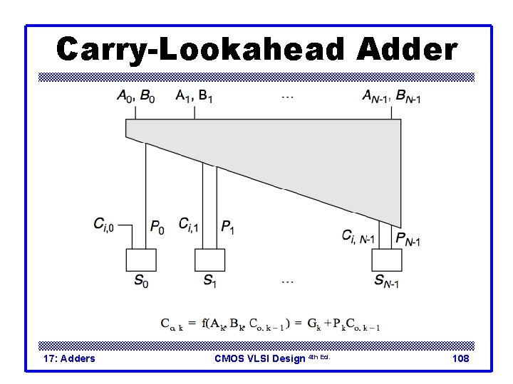
Carry-Lookahead Adder 17: Adders CMOS VLSI Design 4 th Ed. 108

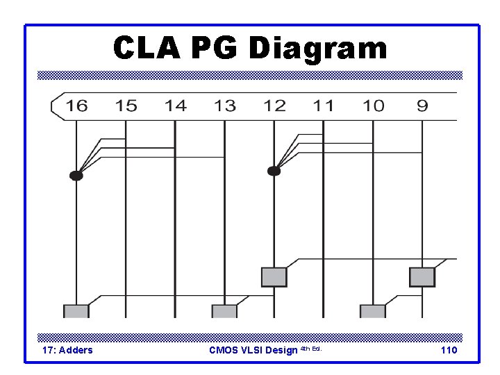
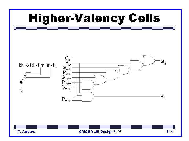
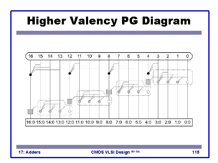
Carry-Lookahead Adder q Carry-lookahead adder computes Gi: 0 for many bits in parallel. q Uses higher-valency cells with more than two inputs. 17: Adders CMOS VLSI Design 4 th Ed. 109

CLA PG Diagram 17: Adders CMOS VLSI Design 4 th Ed. 110

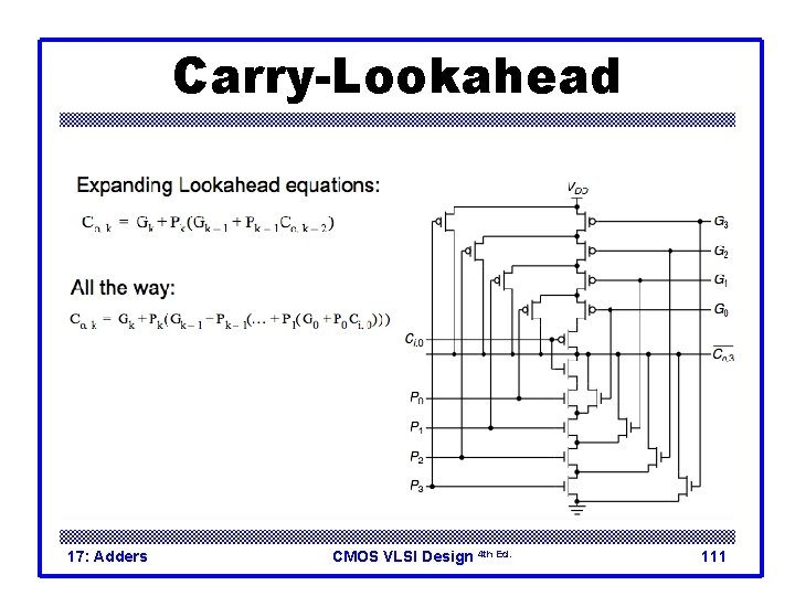
Carry-Lookahead 17: Adders CMOS VLSI Design 4 th Ed. 111

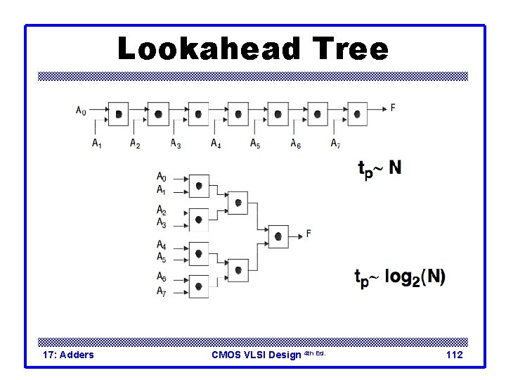
Lookahead Tree 17: Adders CMOS VLSI Design 4 th Ed. 112

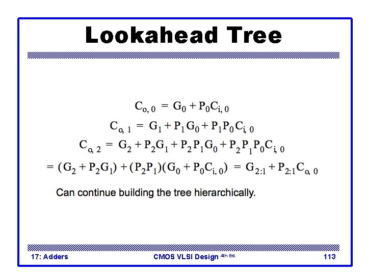
Lookahead Tree 17: Adders CMOS VLSI Design 4 th Ed. 113

Higher-Valency Cells 17: Adders CMOS VLSI Design 4 th Ed. 114

Higher Valency PG Diagram 17: Adders CMOS VLSI Design 4 th Ed. 115

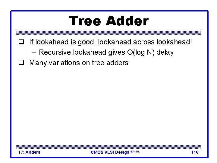
Tree Adder q If lookahead is good, lookahead across lookahead! – Recursive lookahead gives O(log N) delay q Many variations on tree adders 17: Adders CMOS VLSI Design 4 th Ed. 116

Parallel Prefix Adders q Universal adder architecture comprising RCA, CIA, CLA, and more (entire range of area-delay trade-offs from slowest RCA to fastest CLA). q Preprocessing, carry-lookahead, and postprocessing step. q Carries calculated using parallel-prefix algorithms – High regularity: suitable for synthesis and layout – High flexibility: special adders, other arthmetic operations, exchangeable prefix algorithms. – High performance: smallest and fastest adders 17: Adders CMOS VLSI Design 4 th Ed. 117

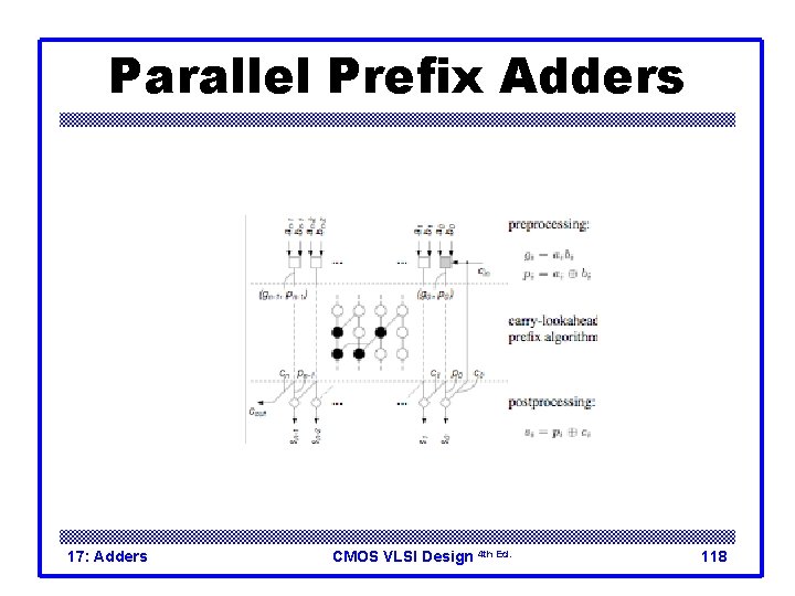
Parallel Prefix Adders 17: Adders CMOS VLSI Design 4 th Ed. 118

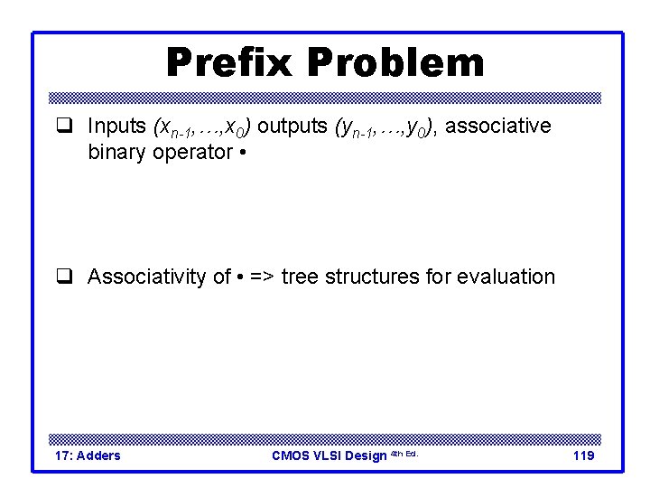
Prefix Problem q Inputs (xn-1, …, x 0) outputs (yn-1, …, y 0), associative binary operator • q Associativity of • => tree structures for evaluation 17: Adders CMOS VLSI Design 4 th Ed. 119

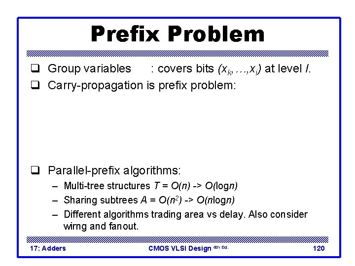
Prefix Problem q Group variables : covers bits (xk, …, xi) at level l. q Carry-propagation is prefix problem: q Parallel-prefix algorithms: – Multi-tree structures T = O(n) -> O(logn) – Sharing subtrees A = O(n 2) -> O(nlogn) – Different algorithms trading area vs delay. Also consider wirng and fanout. 17: Adders CMOS VLSI Design 4 th Ed. 120

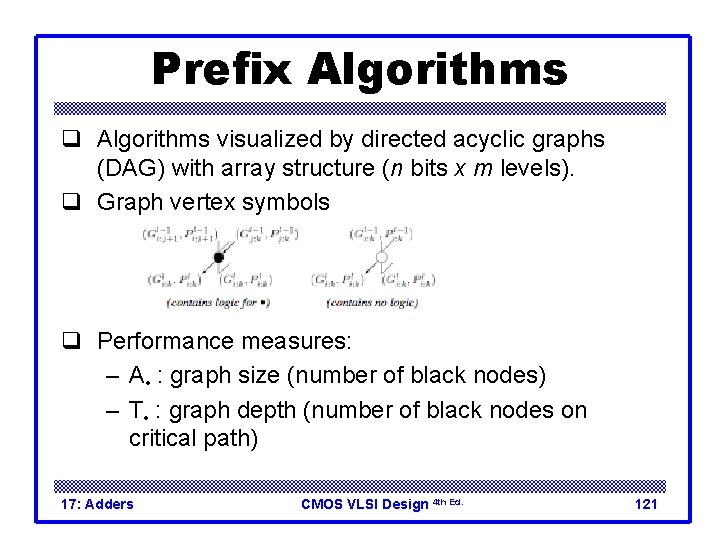
Prefix Algorithms q Algorithms visualized by directed acyclic graphs (DAG) with array structure (n bits x m levels). q Graph vertex symbols q Performance measures: – A • : graph size (number of black nodes) – T • : graph depth (number of black nodes on critical path) 17: Adders CMOS VLSI Design 4 th Ed. 121

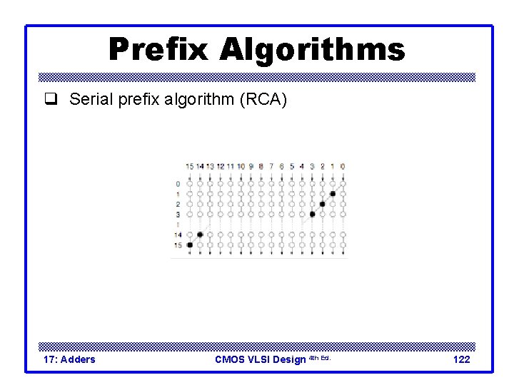
Prefix Algorithms q Serial prefix algorithm (RCA) 17: Adders CMOS VLSI Design 4 th Ed. 122

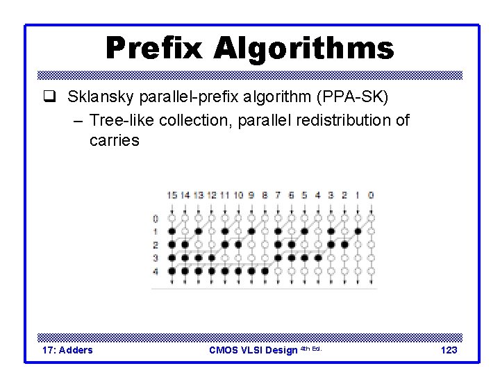
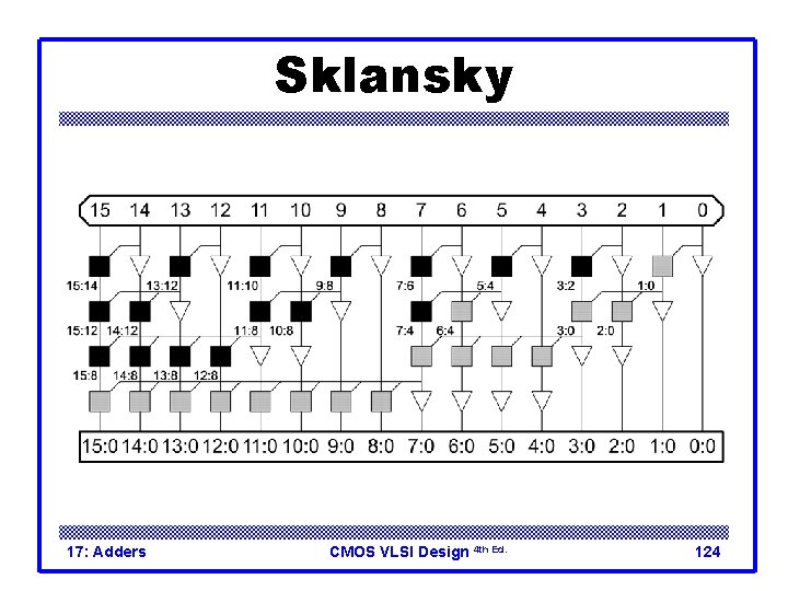
Prefix Algorithms q Sklansky parallel-prefix algorithm (PPA-SK) – Tree-like collection, parallel redistribution of carries 17: Adders CMOS VLSI Design 4 th Ed. 123

Sklansky 17: Adders CMOS VLSI Design 4 th Ed. 124

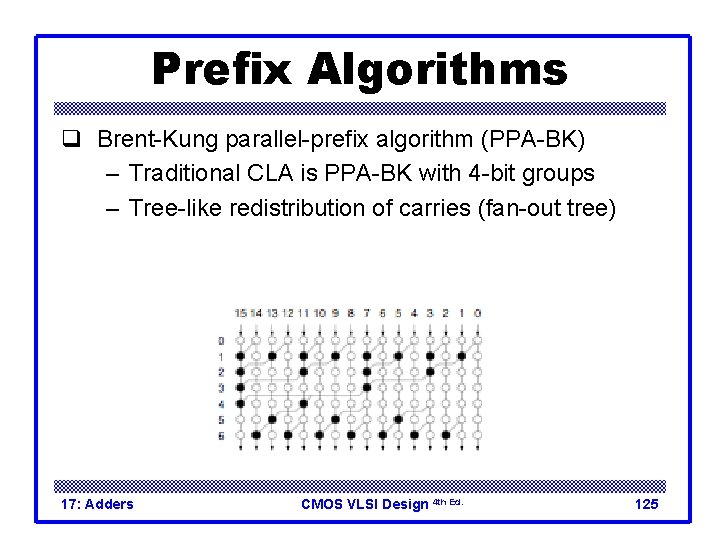
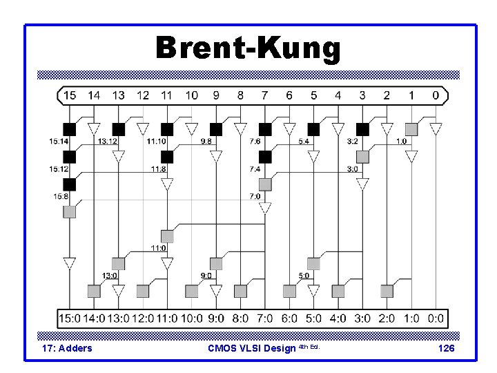
Prefix Algorithms q Brent-Kung parallel-prefix algorithm (PPA-BK) – Traditional CLA is PPA-BK with 4 -bit groups – Tree-like redistribution of carries (fan-out tree) 17: Adders CMOS VLSI Design 4 th Ed. 125

Brent-Kung 17: Adders CMOS VLSI Design 4 th Ed. 126

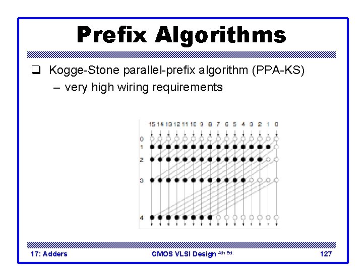
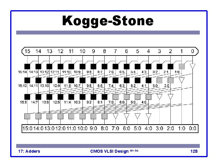
Prefix Algorithms q Kogge-Stone parallel-prefix algorithm (PPA-KS) – very high wiring requirements 17: Adders CMOS VLSI Design 4 th Ed. 127

Kogge-Stone 17: Adders CMOS VLSI Design 4 th Ed. 128

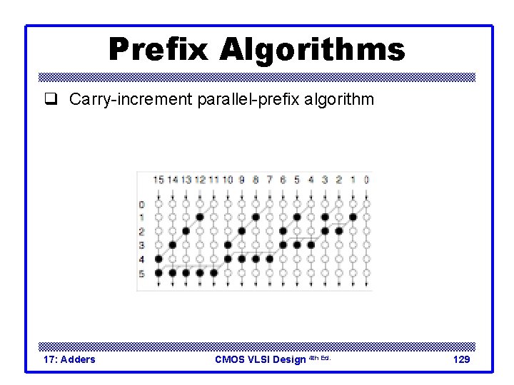
Prefix Algorithms q Carry-increment parallel-prefix algorithm 17: Adders CMOS VLSI Design 4 th Ed. 129

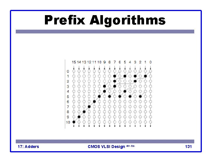
Prefix Algorithms q Mixed serial/parallel-prefix algorithm (RCA+PPA) – Linear size-depth trade-off using parameter k: – k = 0 : serial prefix graph – : Brent-Kung parallel-prefix graph – Fills the gap between RCA and PPA-BK (CLA) in steps of single • -operations. 17: Adders CMOS VLSI Design 4 th Ed. 130

Prefix Algorithms 17: Adders CMOS VLSI Design 4 th Ed. 131

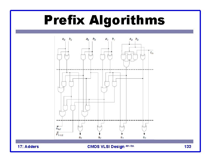
Prefix Algorithms q Example: 4 -bit PPA-SK – Efficient AND-OR-prefix circuit for the generate and AND-prefix circuit for the propagate signals – Optimization: alternatingly AOI/OAI- resp. NAND/NOR-gates (inverting gatesare smaller and faster). – Can also be realized using two MUX-prefix circuits 17: Adders CMOS VLSI Design 4 th Ed. 132

Prefix Algorithms 17: Adders CMOS VLSI Design 4 th Ed. 133

Prefix Algorithms q Prefix adders can be synthesized by human or computer as well. q Starting from a serial structure, one can use compression rules and expansion rules to obtain new graphs. q Can generate all previous graphs except PPA-KS. q Universal adder synthesis approach. 17: Adders CMOS VLSI Design 4 th Ed. 134

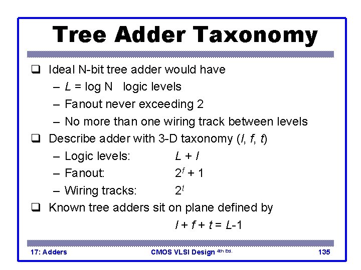
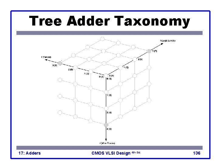
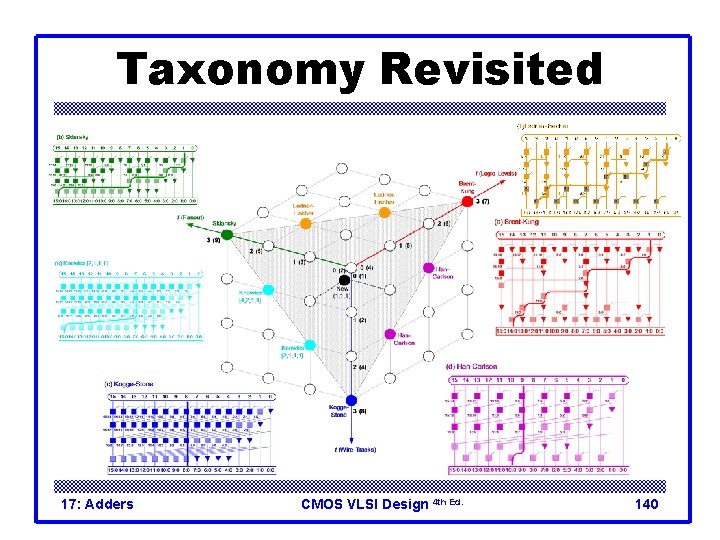
Tree Adder Taxonomy q Ideal N-bit tree adder would have – L = log N logic levels – Fanout never exceeding 2 – No more than one wiring track between levels q Describe adder with 3 -D taxonomy (l, f, t) – Logic levels: L+l – Fanout: 2 f + 1 – Wiring tracks: 2 t q Known tree adders sit on plane defined by l + f + t = L-1 17: Adders CMOS VLSI Design 4 th Ed. 135

Tree Adder Taxonomy 17: Adders CMOS VLSI Design 4 th Ed. 136

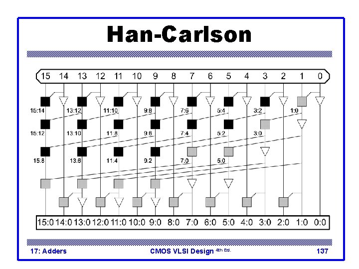
Han-Carlson 17: Adders CMOS VLSI Design 4 th Ed. 137
![Knowles 2 1 1 1 17 Adders CMOS VLSI Design 4 th Ed 138 Knowles [2, 1, 1, 1] 17: Adders CMOS VLSI Design 4 th Ed. 138](https://slidetodoc.com/presentation_image_h/e5efdf22492bfd5d018944a98877a8b2/image-138.jpg)
Knowles [2, 1, 1, 1] 17: Adders CMOS VLSI Design 4 th Ed. 138

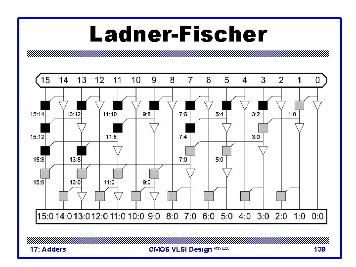
Ladner-Fischer 17: Adders CMOS VLSI Design 4 th Ed. 139

Taxonomy Revisited 17: Adders CMOS VLSI Design 4 th Ed. 140

More Adder Issues q q Multilevel adders – Multilevel versions of adders possible • CSKA, CSLA, CIA Hybrid adders – Arbitrary combination of speed-up techniques possible. – Often used combinations: CLA – CSLA Transistor level adders – Influence of logic styles (dynamic logic, pass transistor logic) – Efficient transistor level implementation of ripple-carry chains (Manchester chain) – Combinations of speed-up techniques make sense. • Much higher design effort – Many efficient implementations exist in the literature. Higher valency (radix) also possible. 17: Adders CMOS VLSI Design 4 th Ed. 141

More Adder Issues q Higher valency is a poor choice in static CMOS logic since each stage has higher delay. q However, if the stages are built using domino logic, it could prove to be an advantage. q Nodes with large fanouts or long wires could use buffers. q The prefix trees can also be internally pipelined. 17: Adders CMOS VLSI Design 4 th Ed. 142

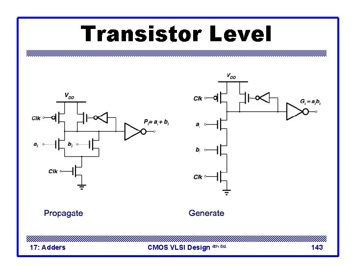
Transistor Level 17: Adders CMOS VLSI Design 4 th Ed. 143

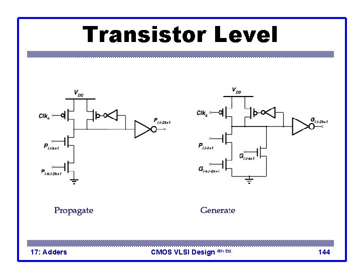
Transistor Level 17: Adders CMOS VLSI Design 4 th Ed. 144

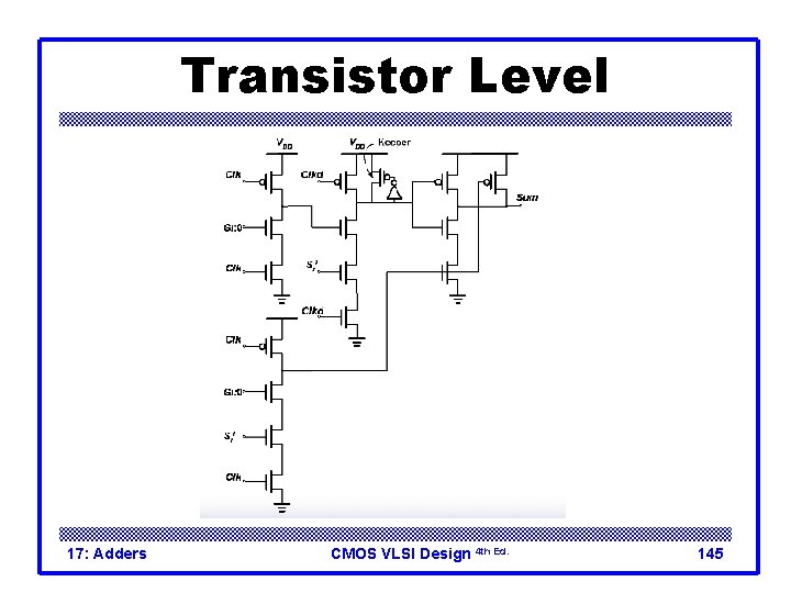
Transistor Level 17: Adders CMOS VLSI Design 4 th Ed. 145

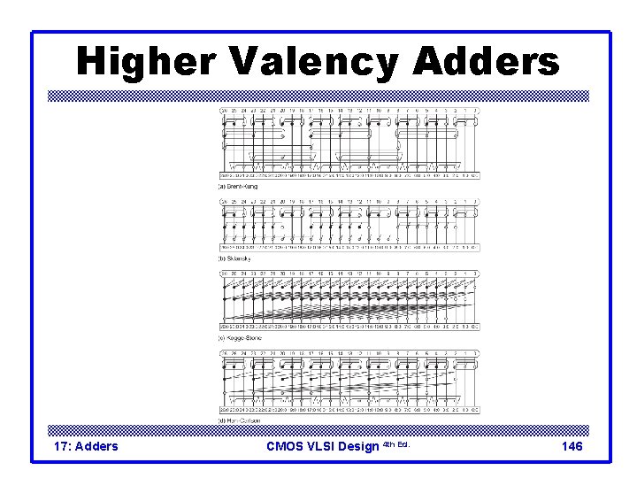
Higher Valency Adders 17: Adders CMOS VLSI Design 4 th Ed. 146

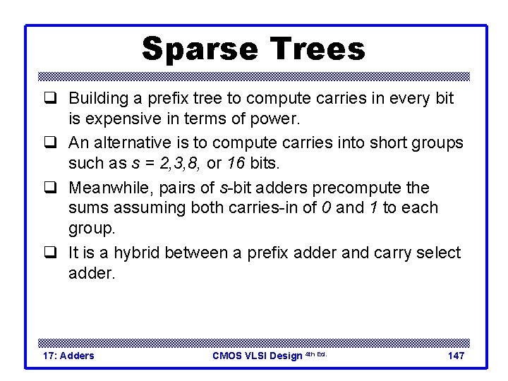
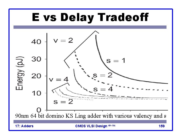
Sparse Trees q Building a prefix tree to compute carries in every bit is expensive in terms of power. q An alternative is to compute carries into short groups such as s = 2, 3, 8, or 16 bits. q Meanwhile, pairs of s-bit adders precompute the sums assuming both carries-in of 0 and 1 to each group. q It is a hybrid between a prefix adder and carry select adder. 17: Adders CMOS VLSI Design 4 th Ed. 147

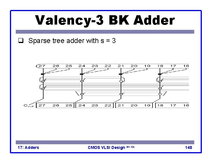
Valency-3 BK Adder q Sparse tree adder with s = 3 17: Adders CMOS VLSI Design 4 th Ed. 148

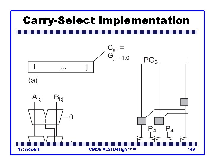
Carry-Select Implementation 17: Adders CMOS VLSI Design 4 th Ed. 149

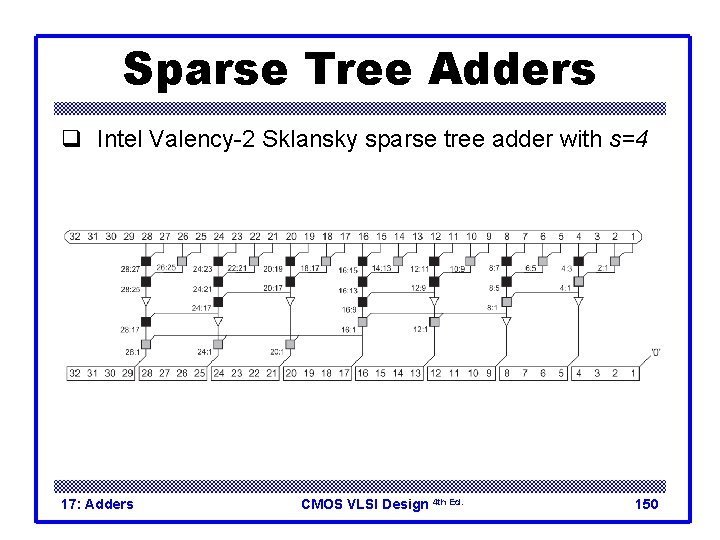
Sparse Tree Adders q Intel Valency-2 Sklansky sparse tree adder with s=4 17: Adders CMOS VLSI Design 4 th Ed. 150

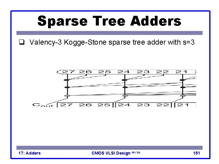
Sparse Tree Adders q Valency-3 Kogge-Stone sparse tree adder with s=3 17: Adders CMOS VLSI Design 4 th Ed. 151

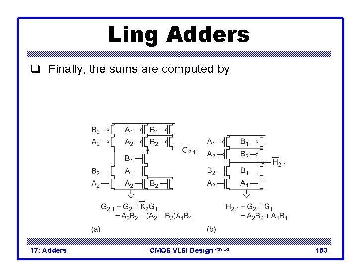
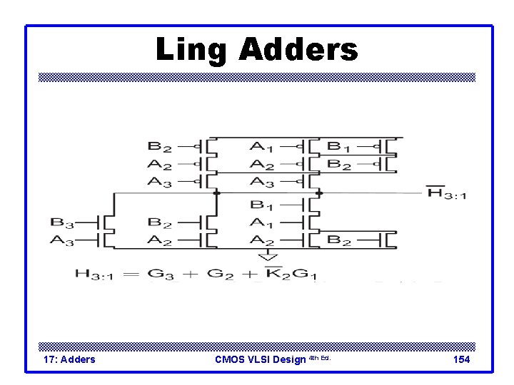
Ling Adders q Ling discovered a technique to remove one series transistor from the critical group generate path at the expense of another XOR gate in the sum precomputation. q Define a pseudo-generate Hi: j = Gi + Gi-1: j This is a simpler computation. q Define a pseudo-propagate signal I that is a shifted version of propagate. 17: Adders CMOS VLSI Design 4 th Ed. 152

Ling Adders q Finally, the sums are computed by 17: Adders CMOS VLSI Design 4 th Ed. 153

Ling Adders 17: Adders CMOS VLSI Design 4 th Ed. 154

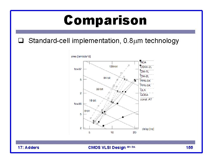
Comparison q Standard-cell implementation, 0. 8 mm technology 17: Adders CMOS VLSI Design 4 th Ed. 155

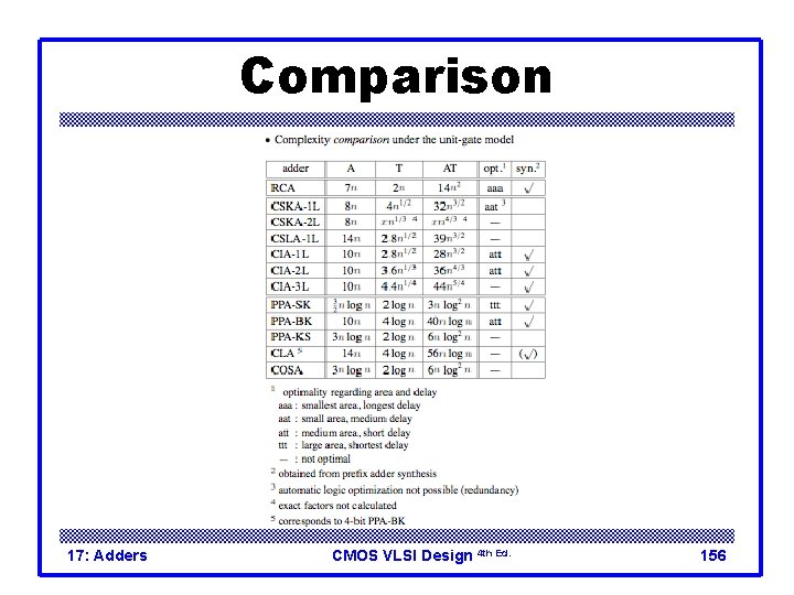
Comparison 17: Adders CMOS VLSI Design 4 th Ed. 156

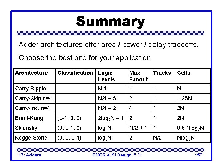
Summary Adder architectures offer area / power / delay tradeoffs. Choose the best one for your application. Architecture Classification Logic Levels Max Fanout Tracks Cells Carry-Ripple N-1 1 1 N Carry-Skip n=4 N/4 + 5 2 1 1. 25 N Carry-Inc. n=4 N/4 + 2 4 1 2 N Brent-Kung (L-1, 0, 0) 2 log 2 N – 1 2 N Sklansky (0, L-1, 0) log 2 N N/2 + 1 1 0. 5 Nlog 2 N Kogge-Stone (0, 0, L-1) log 2 N 2 N/2 Nlog 2 N 17: Adders CMOS VLSI Design 4 th Ed. 157

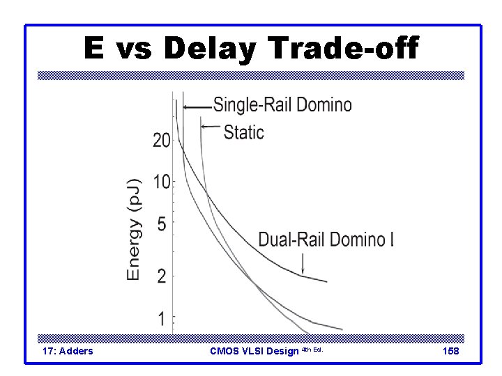
E vs Delay Trade-off 17: Adders CMOS VLSI Design 4 th Ed. 158

E vs Delay Tradeoff 90 nm 64 bit domino KS Ling adder with various valency and s 17: Adders CMOS VLSI Design 4 th Ed. 159

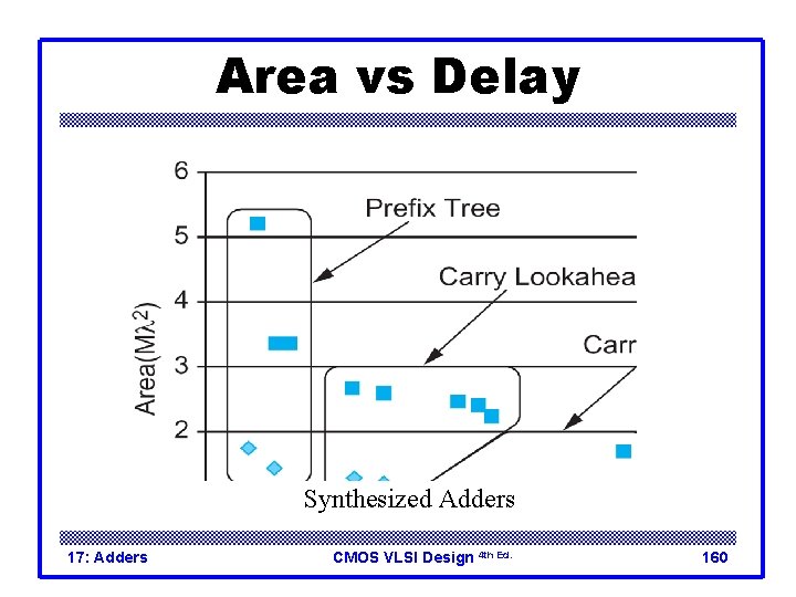
Area vs Delay Synthesized Adders 17: Adders CMOS VLSI Design 4 th Ed. 160