Presentation on Half Adder and Full Adder Under


 0 0 0 1 1 (minterm =A’B) 0")

: INPUT OUTPUT")

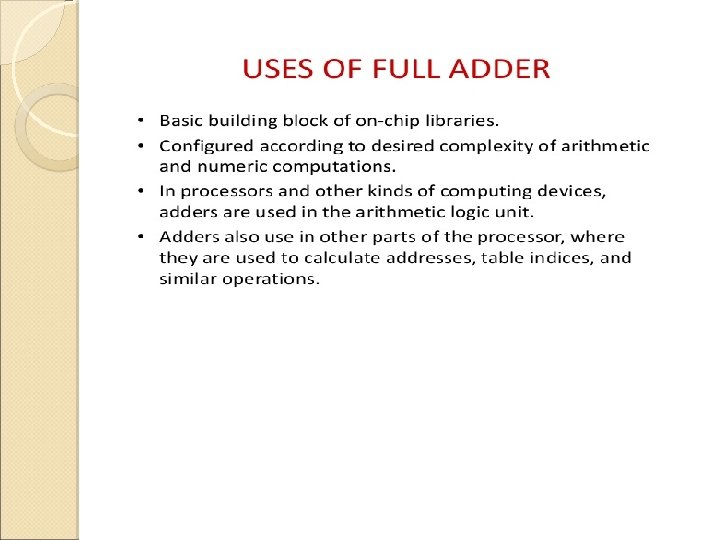
 The ALU (arithmetic logic circuitry) of a computer")


 Carry (C ) 0 0 0 0 1")


- Slides: 16
Presentation on Half Adder and Full Adder Under Work. Shop organised by Department of Physics UOU Haldwani Presented by Manoj Baloni, HOD, Physics S. G. R. R. (P. G. ) College, Dehradun
AIM: To design and construct half adder circuit and verify the truth table using IC/ logic gates. APPARATUS REQUIRED: , Sl. No. COMPONENT SPECIFICATION QTY. 1. AND GATE IC 7408 1 2. X-OR GATE IC 7486 1 3. NOT GATE IC 7404 1 4. OR GATE IC 7432 1 5. IC TRAINER KIT 1
THEORY: A half adder has two inputs for the two bits to be added and two outputs one from the sum ‘ S’ and other from the carry ‘ c’ into the higher adder position. TRUTH TABLE: INPUT OUTPUT A B SUM(S) CARRY( C ) 0 0 0 1 1 0 1 0 1
DESIGN: INPUT OUTPUT A B SUM(S) 0 0 0 1 1 (minterm =A’B) 0 1 (minterm =AB’) 0 1 1 0 1 (minterm=AB) Boolean Equation: SUM : S=A’B+AB’ (EX-OR GATE) CARRY: C=AB CARRY( C )
CIRCUIT DIAGRAM:
PIN DIAGRAM AND GATE (IC 7408 ): INPUT OUTPUT
PIN DIAGRAM EX-OR GATE : INPUT OUTPUT
Application of half Adder circuit: 1) The ALU (arithmetic logic circuitry) of a computer uses half adder to compute the binary addition operation on two bits. 2) Half adder is used to make full adder as a full adder requires 3 inputs, the third input being an input carry i. e. we will be able to cascade the carry bit from one adder to the other. Videio- Link Half Adder - https: //youtu. be/k. KZk. O 61 Jof. Q
AIM: To design and construct Full adder circuit and verify the truth table using IC/ logic gates. APPARATUS REQUIRED: Sl. No. COMPONENT SPECIFICATION QTY. 1. AND GATE IC 7408 1 2. X-OR GATE IC 7486 1 3. NOT GATE IC 7404 1 4. OR GATE IC 7432 1 5. IC TRAINER KIT 1
THEORY: A full adder is a combinational circuit that forms the arithmetic sum of input; it consists of three inputs and two outputs. A full adder is useful to add three bits at a time but a half adder cannot do so. TRUTH TABLE: A B C Sum (S) Carry (C ) 0 0 0 0 1 1 0 0 1 0 1 1 1 0 0 1 1 1
DESIGN: A B C Sum (S) Carry (C ) 0 0 0 0 1 1(minterm=A’B’C) 0 0 1(minterm=A’BC’) 0 0 1 1 0 0 1(minterm=AB’C’) 0 1 0 1(minterm=AB’C ) 1 1 0 0 1(minterm=ABC’ ) 1 1(minterm=ABC) 1 Boolean Equation: 1 SUM : S= A’B’C+A’B C’+AB’C’+ABC (EX-OR GATE) CARRY: C=A’BC+AB’C+ABC’+ABC Reducing by K-Map C=AB+BC+CA 1(minterm=A’BC )
CIRCUIT DIAGRAM:
PIN DIAGRAM OR GATE: INPUT OUTPUT
Example 0 1 Cout 1 0 0 sum Vedio-Link https: //youtu. be/b. G 2 xqg. F 2 lz. M 1 C in
Thank you