Introduction to CMOS VLSI Design Adders 1 Outline
![Knowles [2, 1, 1, 1] Adders CMOS VLSI Design 41 Knowles [2, 1, 1, 1] Adders CMOS VLSI Design 41](https://slidetodoc.com/presentation_image_h/c163c6e36e085066e3076ae36787591f/image-41.jpg)
- Slides: 44

Introduction to CMOS VLSI Design Adders 1

Outline q q q q Single-bit Addition Carry-Ripple Adder Carry-Skip Adder Carry-Lookahead Adder Carry-Select Adder Carry-Increment Adder Tree Adders CMOS VLSI Design 2

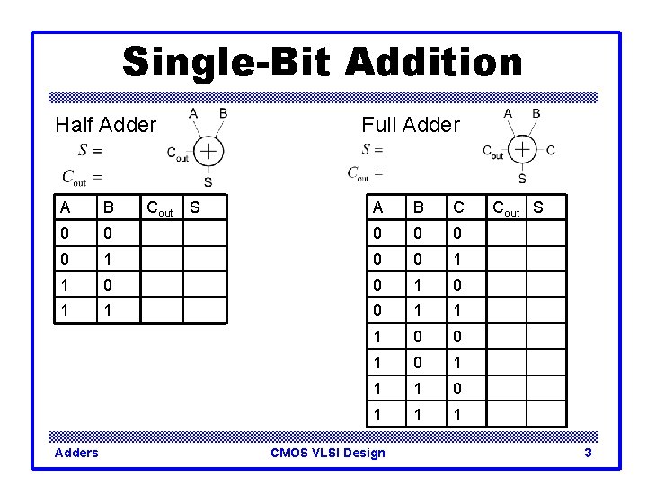
Single-Bit Addition Half Adder A B 0 A B C 0 0 0 1 0 1 1 1 0 1 1 1 Adders Cout Full Adder S CMOS VLSI Design Cout S 3

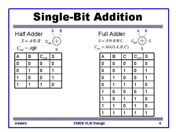
Single-Bit Addition Half Adder Full Adder A B Cout S A B C Cout S 0 0 0 0 0 1 0 0 1 1 0 0 1 1 1 0 0 0 1 1 0 1 1 1 Adders CMOS VLSI Design 4

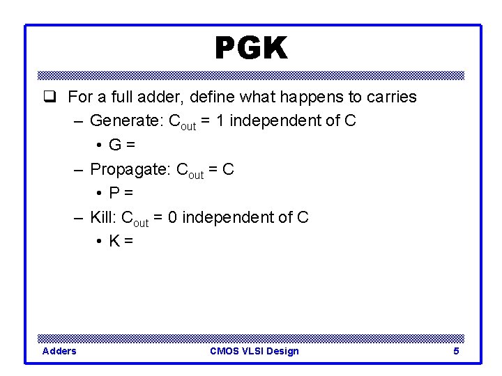
PGK q For a full adder, define what happens to carries – Generate: Cout = 1 independent of C • G= – Propagate: Cout = C • P= – Kill: Cout = 0 independent of C • K= Adders CMOS VLSI Design 5

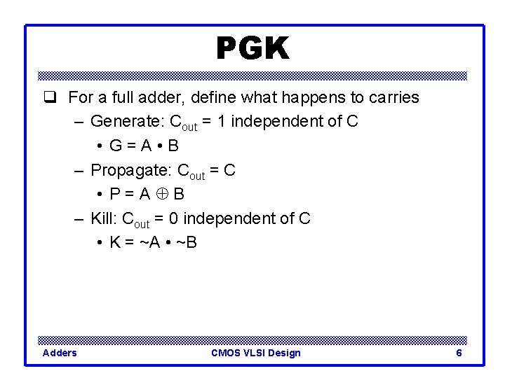
PGK q For a full adder, define what happens to carries – Generate: Cout = 1 independent of C • G=A • B – Propagate: Cout = C • P=A B – Kill: Cout = 0 independent of C • K = ~A • ~B Adders CMOS VLSI Design 6

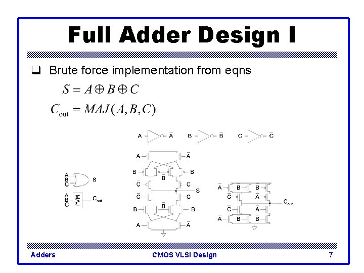
Full Adder Design I q Brute force implementation from eqns Adders CMOS VLSI Design 7

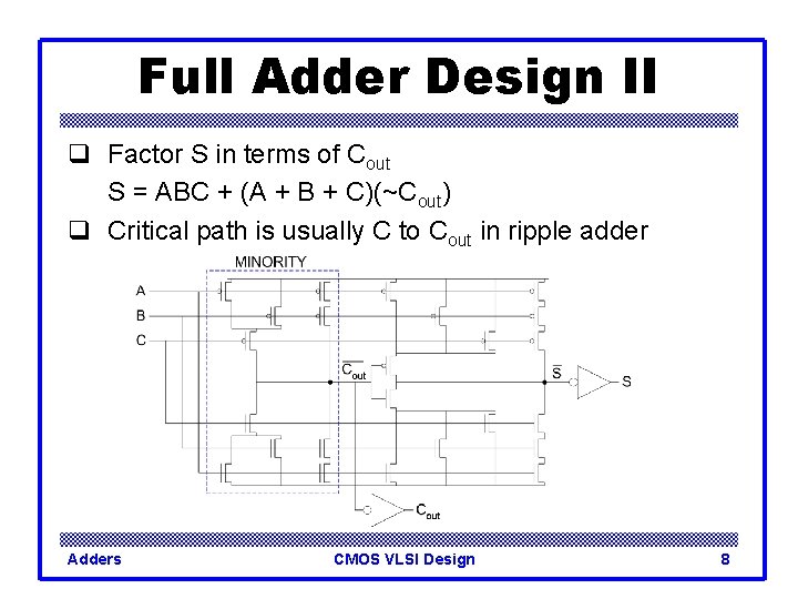
Full Adder Design II q Factor S in terms of Cout S = ABC + (A + B + C)(~Cout) q Critical path is usually C to Cout in ripple adder Adders CMOS VLSI Design 8

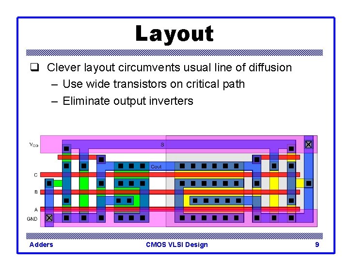
Layout q Clever layout circumvents usual line of diffusion – Use wide transistors on critical path – Eliminate output inverters Adders CMOS VLSI Design 9

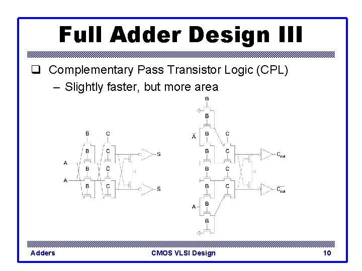
Full Adder Design III q Complementary Pass Transistor Logic (CPL) – Slightly faster, but more area Adders CMOS VLSI Design 10

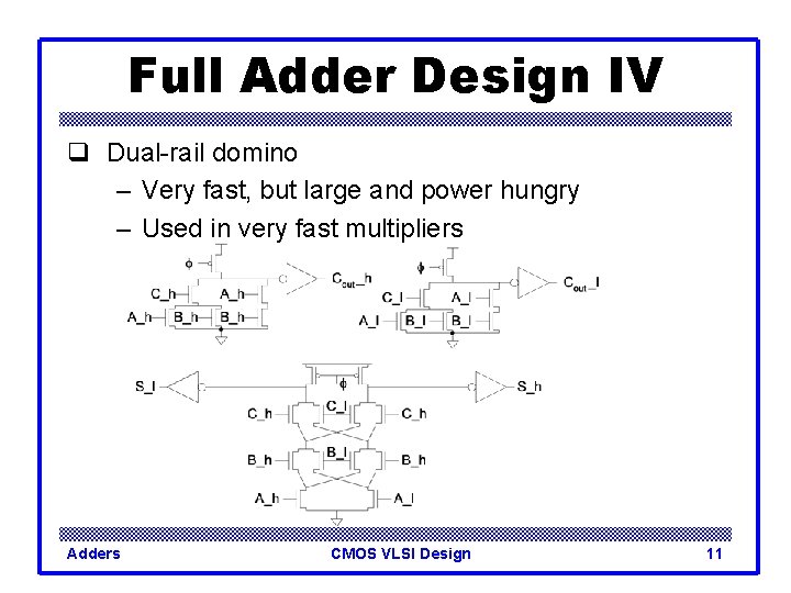
Full Adder Design IV q Dual-rail domino – Very fast, but large and power hungry – Used in very fast multipliers Adders CMOS VLSI Design 11

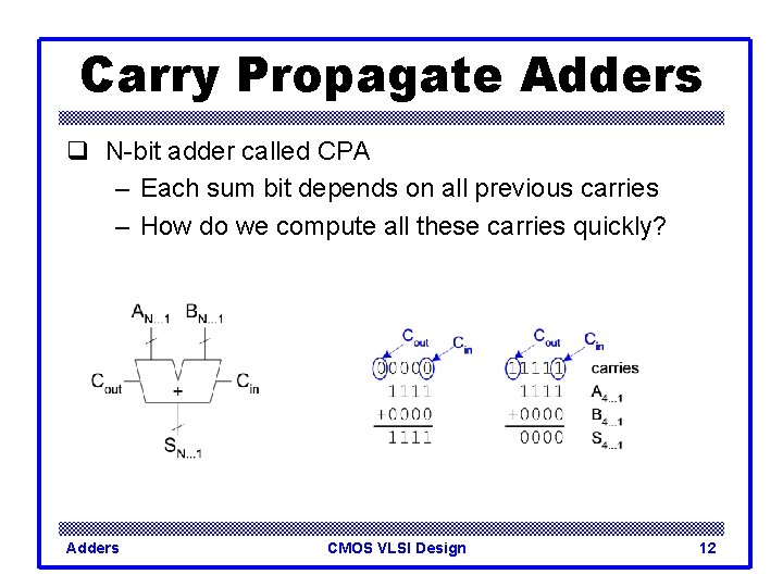
Carry Propagate Adders q N-bit adder called CPA – Each sum bit depends on all previous carries – How do we compute all these carries quickly? Adders CMOS VLSI Design 12

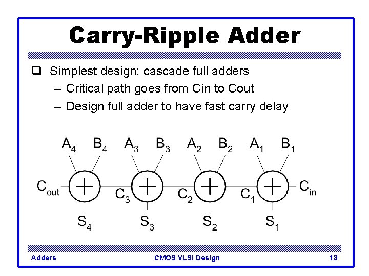
Carry-Ripple Adder q Simplest design: cascade full adders – Critical path goes from Cin to Cout – Design full adder to have fast carry delay Adders CMOS VLSI Design 13

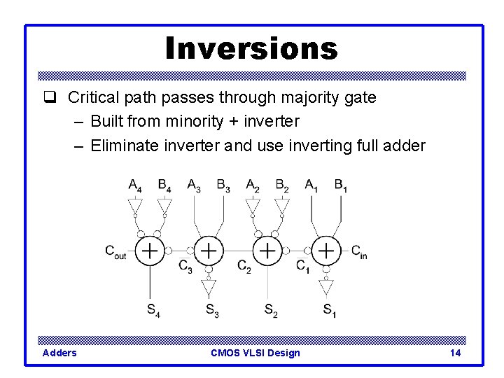
Inversions q Critical path passes through majority gate – Built from minority + inverter – Eliminate inverter and use inverting full adder Adders CMOS VLSI Design 14

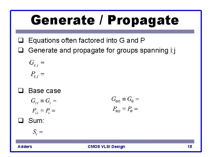
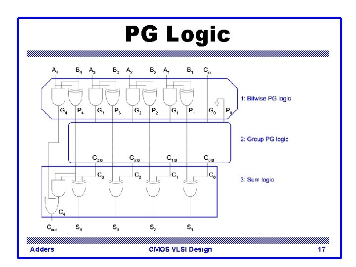
Generate / Propagate q Equations often factored into G and P q Generate and propagate for groups spanning i: j q Base case q Sum: Adders CMOS VLSI Design 15

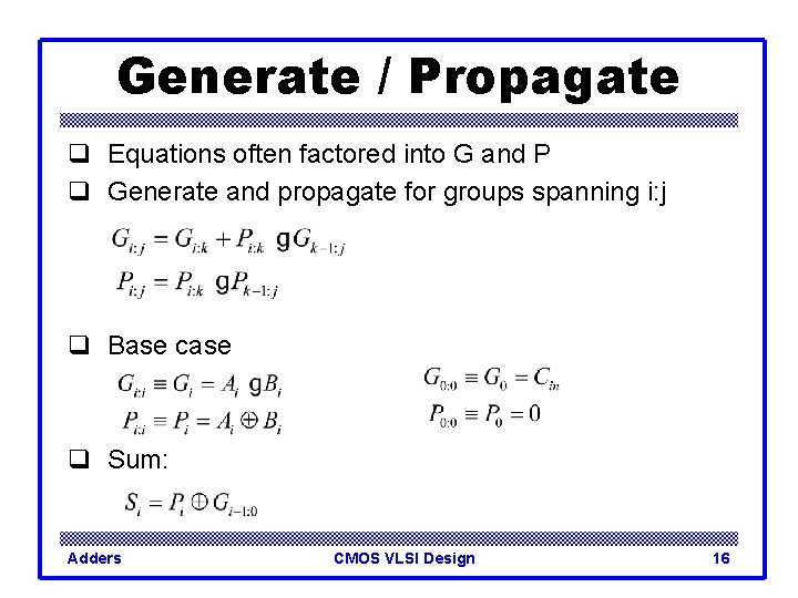
Generate / Propagate q Equations often factored into G and P q Generate and propagate for groups spanning i: j q Base case q Sum: Adders CMOS VLSI Design 16

PG Logic Adders CMOS VLSI Design 17

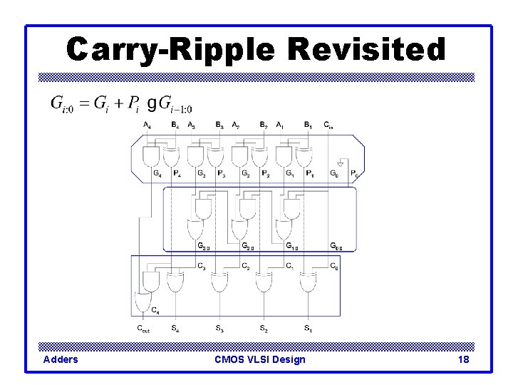
Carry-Ripple Revisited Adders CMOS VLSI Design 18

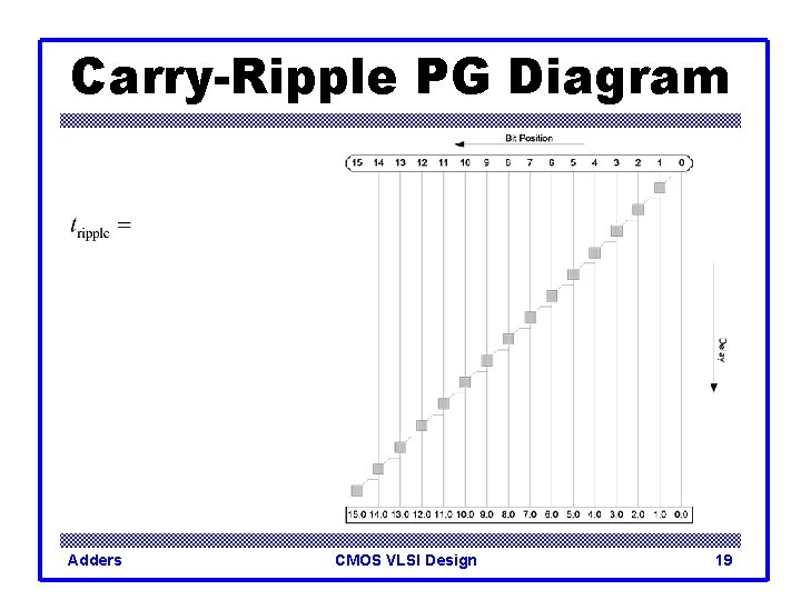
Carry-Ripple PG Diagram Adders CMOS VLSI Design 19

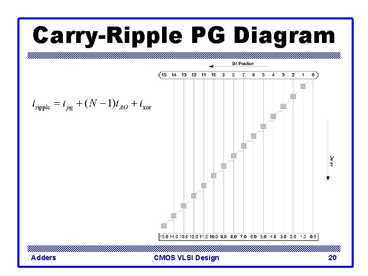
Carry-Ripple PG Diagram Adders CMOS VLSI Design 20

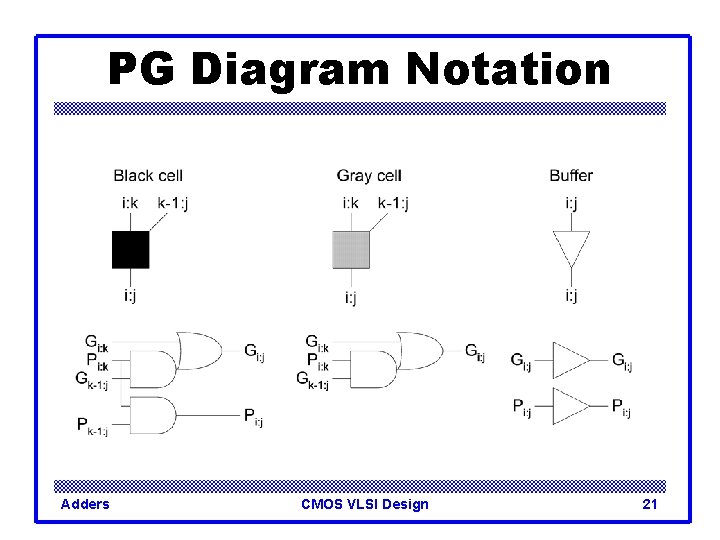
PG Diagram Notation Adders CMOS VLSI Design 21

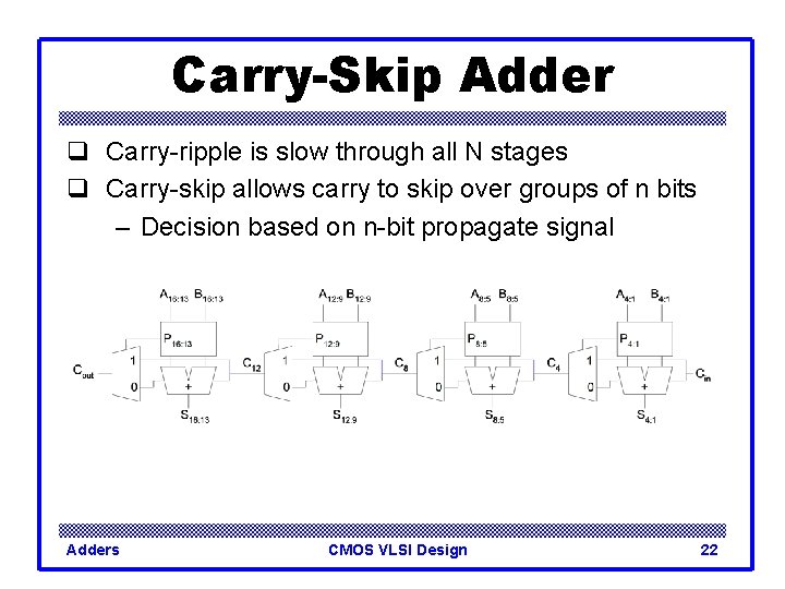
Carry-Skip Adder q Carry-ripple is slow through all N stages q Carry-skip allows carry to skip over groups of n bits – Decision based on n-bit propagate signal Adders CMOS VLSI Design 22

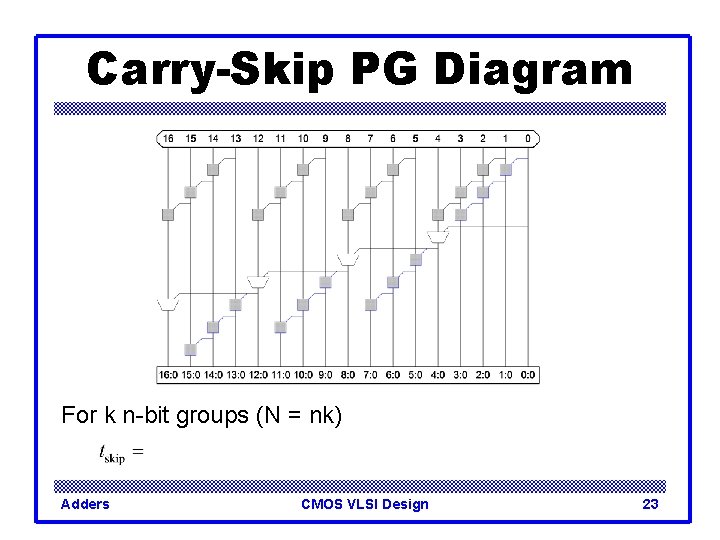
Carry-Skip PG Diagram For k n-bit groups (N = nk) Adders CMOS VLSI Design 23

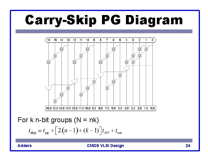
Carry-Skip PG Diagram For k n-bit groups (N = nk) Adders CMOS VLSI Design 24

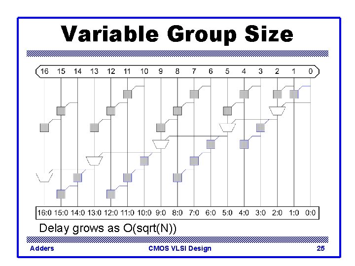
Variable Group Size Delay grows as O(sqrt(N)) Adders CMOS VLSI Design 25

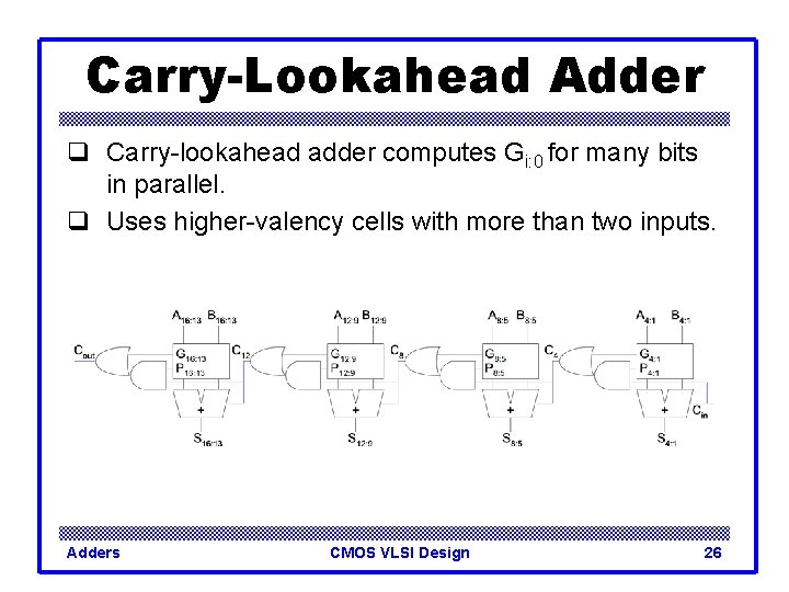
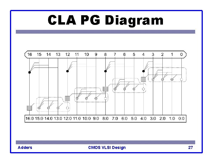
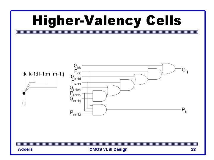
Carry-Lookahead Adder q Carry-lookahead adder computes Gi: 0 for many bits in parallel. q Uses higher-valency cells with more than two inputs. Adders CMOS VLSI Design 26

CLA PG Diagram Adders CMOS VLSI Design 27

Higher-Valency Cells Adders CMOS VLSI Design 28

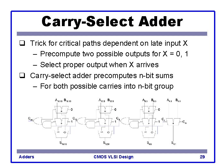
Carry-Select Adder q Trick for critical paths dependent on late input X – Precompute two possible outputs for X = 0, 1 – Select proper output when X arrives q Carry-select adder precomputes n-bit sums – For both possible carries into n-bit group Adders CMOS VLSI Design 29

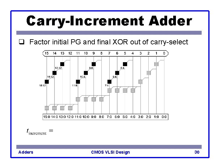
Carry-Increment Adder q Factor initial PG and final XOR out of carry-select Adders CMOS VLSI Design 30

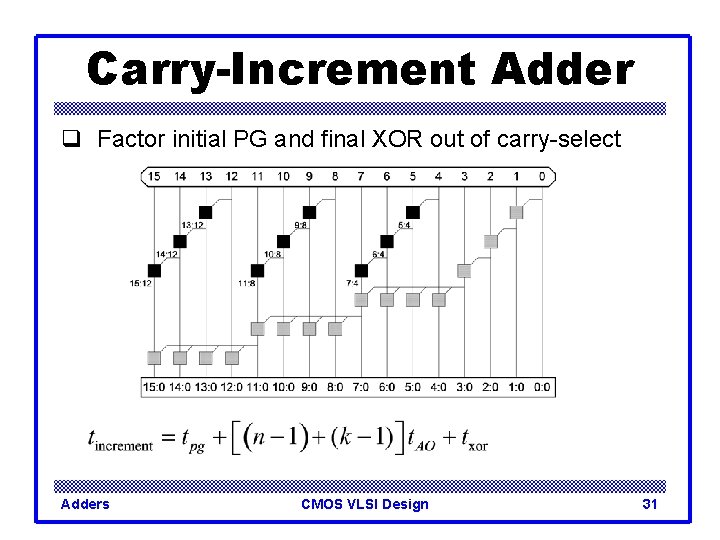
Carry-Increment Adder q Factor initial PG and final XOR out of carry-select Adders CMOS VLSI Design 31

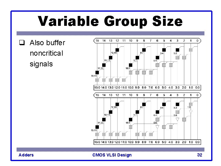
Variable Group Size q Also buffer noncritical signals Adders CMOS VLSI Design 32

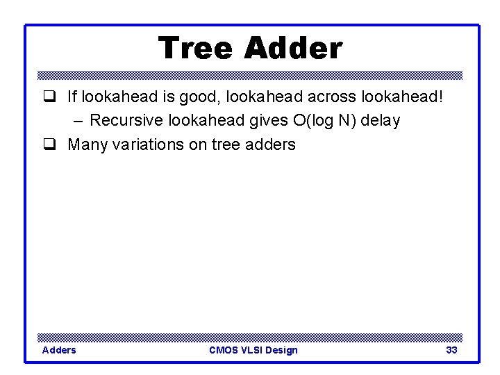
Tree Adder q If lookahead is good, lookahead across lookahead! – Recursive lookahead gives O(log N) delay q Many variations on tree adders Adders CMOS VLSI Design 33

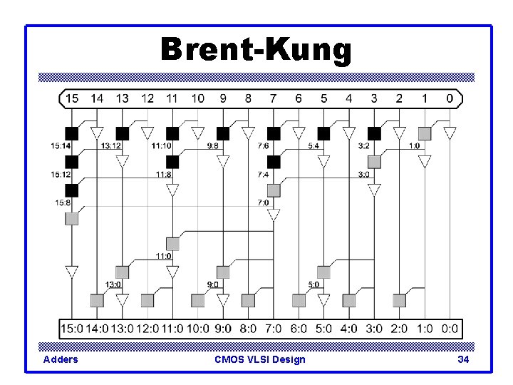
Brent-Kung Adders CMOS VLSI Design 34

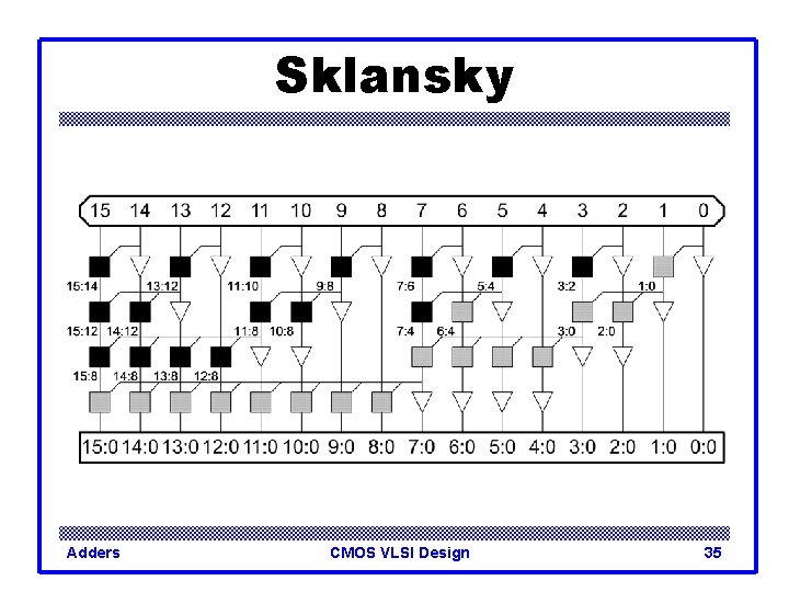
Sklansky Adders CMOS VLSI Design 35

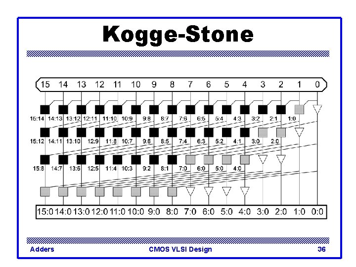
Kogge-Stone Adders CMOS VLSI Design 36

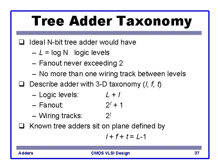
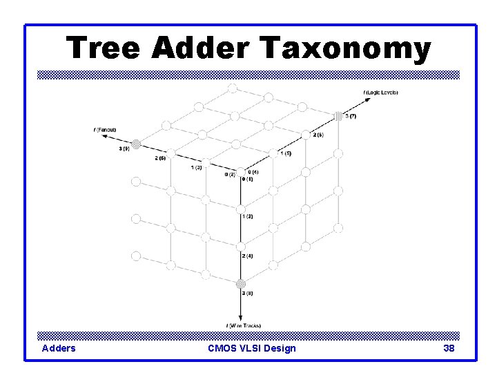
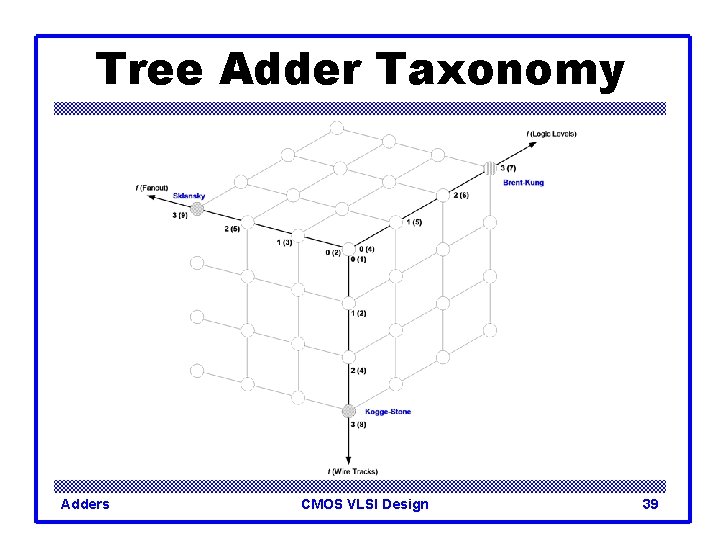
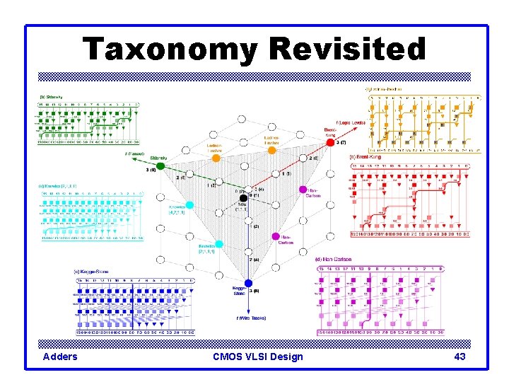
Tree Adder Taxonomy q Ideal N-bit tree adder would have – L = log N logic levels – Fanout never exceeding 2 – No more than one wiring track between levels q Describe adder with 3 -D taxonomy (l, f, t) – Logic levels: L+l – Fanout: 2 f + 1 – Wiring tracks: 2 t q Known tree adders sit on plane defined by l + f + t = L-1 Adders CMOS VLSI Design 37

Tree Adder Taxonomy Adders CMOS VLSI Design 38

Tree Adder Taxonomy Adders CMOS VLSI Design 39

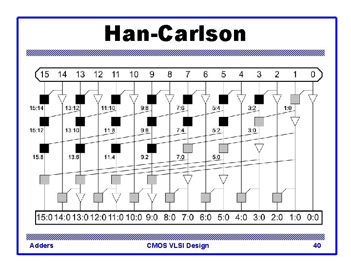
Han-Carlson Adders CMOS VLSI Design 40
![Knowles 2 1 1 1 Adders CMOS VLSI Design 41 Knowles [2, 1, 1, 1] Adders CMOS VLSI Design 41](https://slidetodoc.com/presentation_image_h/c163c6e36e085066e3076ae36787591f/image-41.jpg)
Knowles [2, 1, 1, 1] Adders CMOS VLSI Design 41

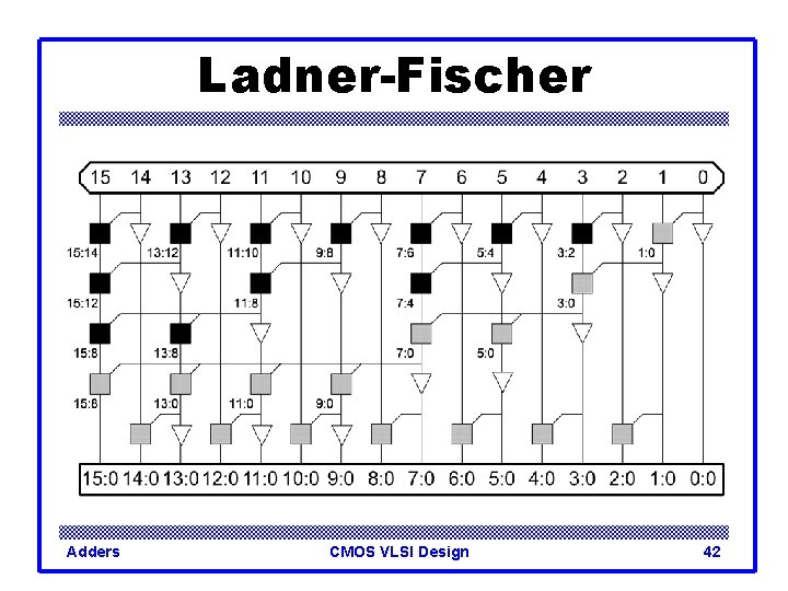
Ladner-Fischer Adders CMOS VLSI Design 42

Taxonomy Revisited Adders CMOS VLSI Design 43

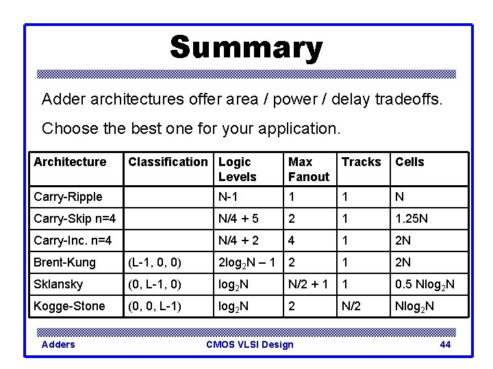
Summary Adder architectures offer area / power / delay tradeoffs. Choose the best one for your application. Architecture Classification Logic Levels Max Fanout Tracks Cells Carry-Ripple N-1 1 1 N Carry-Skip n=4 N/4 + 5 2 1 1. 25 N Carry-Inc. n=4 N/4 + 2 4 1 2 N Brent-Kung (L-1, 0, 0) 2 log 2 N – 1 2 N Sklansky (0, L-1, 0) log 2 N N/2 + 1 1 0. 5 Nlog 2 N Kogge-Stone (0, 0, L-1) log 2 N 2 N/2 Nlog 2 N Adders CMOS VLSI Design 44