LowPower Electronics and Systems Vishwani D Agrawal James
![i(t) = C dv(t)/dt = [V – v(t)] /R dv(t) V – v(t) ─── i(t) = C dv(t)/dt = [V – v(t)] /R dv(t) V – v(t) ───](https://slidetodoc.com/presentation_image_h/8214a8e0100fbfd18560c29c4ac673be/image-18.jpg)
![v(t) = i(t) August 9, 2006 = -t V [1 – exp( ── )] v(t) = i(t) August 9, 2006 = -t V [1 – exp( ── )]](https://slidetodoc.com/presentation_image_h/8214a8e0100fbfd18560c29c4ac673be/image-19.jpg)
![isc and Output Capacitance Isc(t) = August 9, 2006 -t VDD[1 - exp(─────)] vo(t) isc and Output Capacitance Isc(t) = August 9, 2006 -t VDD[1 - exp(─────)] vo(t)](https://slidetodoc.com/presentation_image_h/8214a8e0100fbfd18560c29c4ac673be/image-28.jpg)

- Slides: 118

Low-Power Electronics and Systems Vishwani D. Agrawal James J. Danaher Professor Department of Electrical and Computer Engineering Auburn University, Auburn, AL 36849, USA http: //www. eng. auburn. edu/~vagrawal@eng. auburn. edu August 9, 2006 Agrawal: VDAT'06 Tutorial II 1

Contents • Introduction • Dynamic power – Short circuit power – Reduced supply voltage operation – Glitch elimination • Static (leakage) power reduction • Low power systems – State encoding – Processor and multi-core design • Books on low-power design August 9, 2006 Agrawal: VDAT'06 Tutorial II 2

Introduction Power Consumption of VLSI Chips Why is it a concern? August 9, 2006 Agrawal: VDAT'06 Tutorial II 3

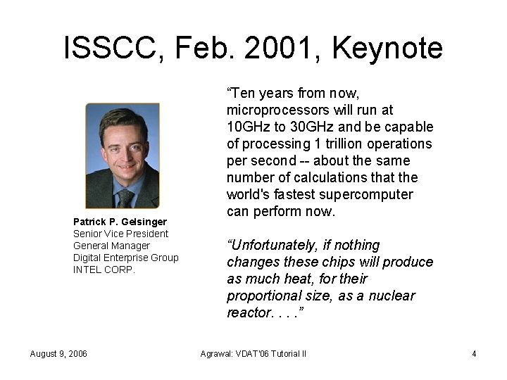
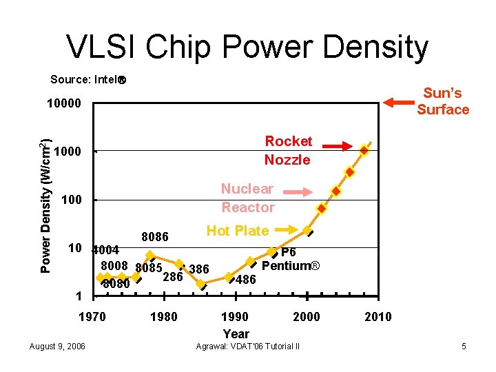
ISSCC, Feb. 2001, Keynote Patrick P. Gelsinger Senior Vice President General Manager Digital Enterprise Group INTEL CORP. August 9, 2006 “Ten years from now, microprocessors will run at 10 GHz to 30 GHz and be capable of processing 1 trillion operations per second -- about the same number of calculations that the world's fastest supercomputer can perform now. “Unfortunately, if nothing changes these chips will produce as much heat, for their proportional size, as a nuclear reactor. . ” Agrawal: VDAT'06 Tutorial II 4

VLSI Chip Power Density Source: Intel Sun’s Surface Power Density (W/cm 2) 10000 Rocket Nozzle 1000 Nuclear Reactor 100 8086 Hot Plate 10 4004 8008 8085 386 286 8080 1 1970 August 9, 2006 1980 P 6 Pentium® 486 1990 Year 2000 Agrawal: VDAT'06 Tutorial II 2010 5

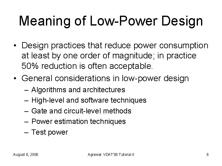
Meaning of Low-Power Design • Design practices that reduce power consumption at least by one order of magnitude; in practice 50% reduction is often acceptable. • General considerations in low-power design – – – Algorithms and architectures High-level and software techniques Gate and circuit-level methods Power estimation techniques Test power August 9, 2006 Agrawal: VDAT'06 Tutorial II 6

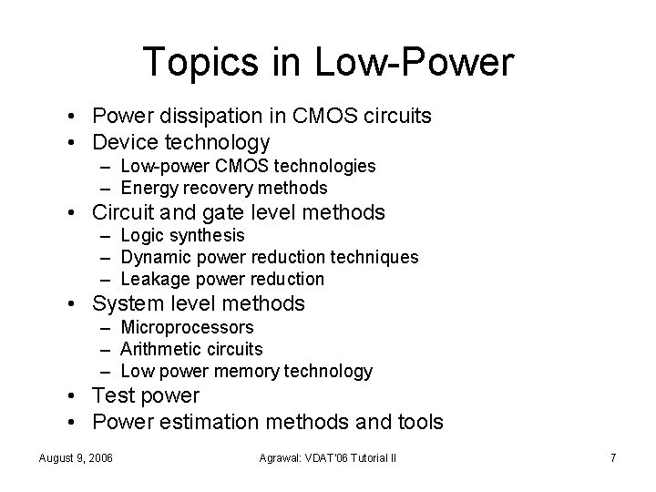
Topics in Low-Power • Power dissipation in CMOS circuits • Device technology – Low-power CMOS technologies – Energy recovery methods • Circuit and gate level methods – Logic synthesis – Dynamic power reduction techniques – Leakage power reduction • System level methods – Microprocessors – Arithmetic circuits – Low power memory technology • Test power • Power estimation methods and tools August 9, 2006 Agrawal: VDAT'06 Tutorial II 7

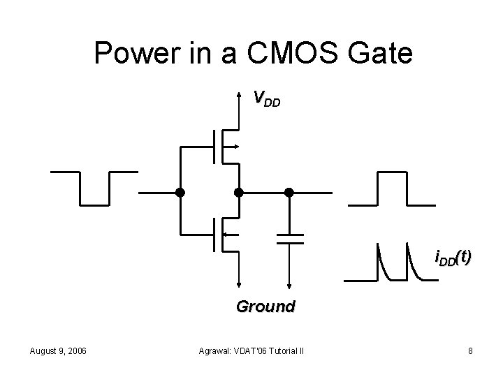
Power in a CMOS Gate VDD i. DD(t) Ground August 9, 2006 Agrawal: VDAT'06 Tutorial II 8

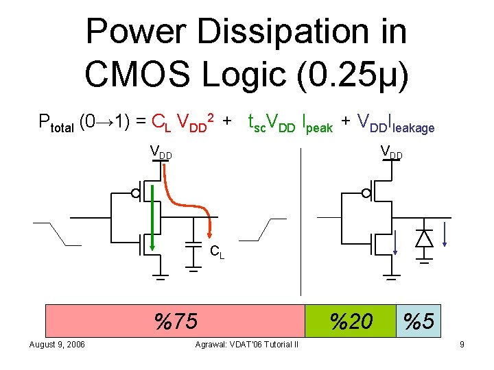
Power Dissipation in CMOS Logic (0. 25µ) Ptotal (0→ 1) = CL VDD 2 + tsc. VDD Ipeak + VDDIleakage VDD CL %75 August 9, 2006 Agrawal: VDAT'06 Tutorial II %20 %5 9

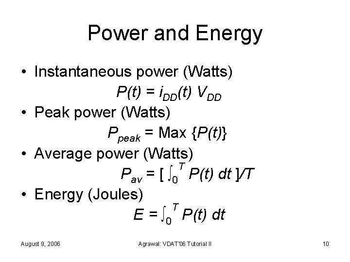
Power and Energy • Instantaneous power (Watts) P(t) = i. DD(t) VDD • Peak power (Watts) Ppeak = Max {P(t)} • Average power (Watts) T Pav = [ ∫ 0 P(t) dt ]/T • Energy (Joules) T E = ∫ 0 P(t) dt August 9, 2006 Agrawal: VDAT'06 Tutorial II 10

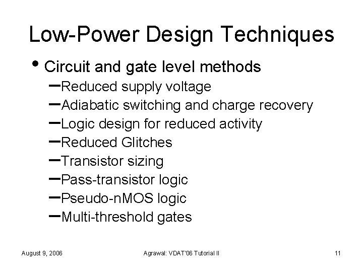
Low-Power Design Techniques • Circuit and gate level methods –Reduced supply voltage –Adiabatic switching and charge recovery –Logic design for reduced activity –Reduced Glitches –Transistor sizing –Pass-transistor logic –Pseudo-n. MOS logic –Multi-threshold gates August 9, 2006 Agrawal: VDAT'06 Tutorial II 11

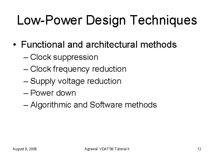
Low-Power Design Techniques • Functional and architectural methods – Clock suppression – Clock frequency reduction – Supply voltage reduction – Power down – Algorithmic and Software methods August 9, 2006 Agrawal: VDAT'06 Tutorial II 12

Test Power • Power grid on a VLSI chip is designed for certain current capacity during functional operation: – Average current → heat dissipation – Peak current → noise, ground bounce • Problem – Tests like scan or BIST are nonfunctional and may cause higher than the functional circuit activity; a functionally good chip can fail the test. August 9, 2006 Agrawal: VDAT'06 Tutorial II 13

Power Estimation Methods • Spice: Accurate but expensive • Logic-level – Event-driven simulation – Statistical – Probabilistic • High-level: Hierarchical August 9, 2006 Agrawal: VDAT'06 Tutorial II 14

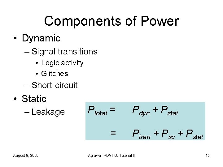
Components of Power • Dynamic – Signal transitions • Logic activity • Glitches – Short-circuit • Static – Leakage Ptotal = = August 9, 2006 Pdyn + Pstat Ptran + Psc + Pstat Agrawal: VDAT'06 Tutorial II 15

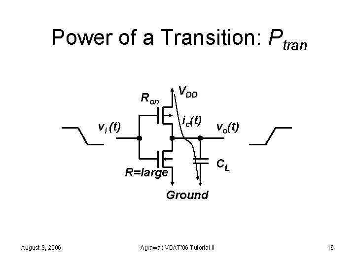
Power of a Transition: Ptran VDD Ron ic(t) vi (t) R=large vo(t) CL Ground August 9, 2006 Agrawal: VDAT'06 Tutorial II 16

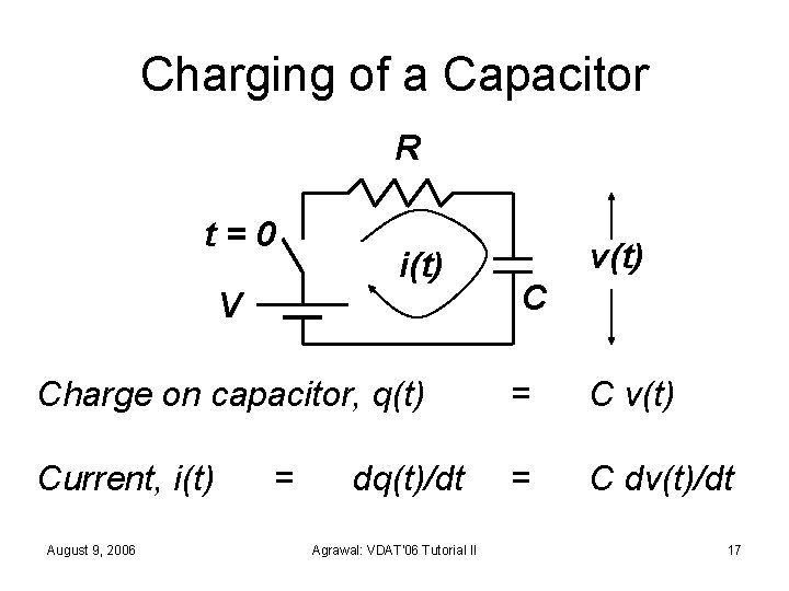
Charging of a Capacitor R t=0 i(t) V v(t) C Charge on capacitor, q(t) = C v(t) Current, i(t) = C dv(t)/dt August 9, 2006 = dq(t)/dt Agrawal: VDAT'06 Tutorial II 17
![it C dvtdt V vt R dvt V vt i(t) = C dv(t)/dt = [V – v(t)] /R dv(t) V – v(t) ───](https://slidetodoc.com/presentation_image_h/8214a8e0100fbfd18560c29c4ac673be/image-18.jpg)
i(t) = C dv(t)/dt = [V – v(t)] /R dv(t) V – v(t) ─── = ───── dt RC dv(t) dt ∫ ───── = ∫───── V – v(t) RC -t ln [V – v(t)] = ── + A RC Initial condition, t = 0, v(t) = 0 → A = ln V -t v(t) = V [1 – exp(───)] RC August 9, 2006 Agrawal: VDAT'06 Tutorial II 18
![vt it August 9 2006 t V 1 exp v(t) = i(t) August 9, 2006 = -t V [1 – exp( ── )]](https://slidetodoc.com/presentation_image_h/8214a8e0100fbfd18560c29c4ac673be/image-19.jpg)
v(t) = i(t) August 9, 2006 = -t V [1 – exp( ── )] RC dv(t) C ─── dt = Agrawal: VDAT'06 Tutorial II V -t ── exp( ── ) R RC 19

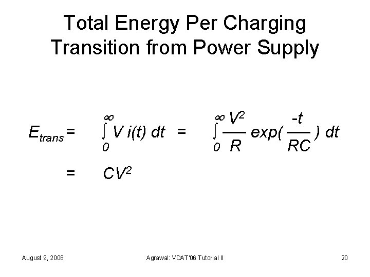
Total Energy Per Charging Transition from Power Supply Etrans = = August 9, 2006 ∞ ∫ V i(t) dt = 0 ∞ V 2 -t ∫ ── exp( ── ) dt 0 R RC CV 2 Agrawal: VDAT'06 Tutorial II 20

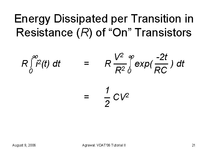
Energy Dissipated per Transition in Resistance (R) of “On” Transistors ∞ 2 R ∫ i (t) dt 0 August 9, 2006 = V 2 ∞ -2 t R ── ∫ exp( ── ) dt R 2 0 RC = 1 ─ CV 2 2 Agrawal: VDAT'06 Tutorial II 21

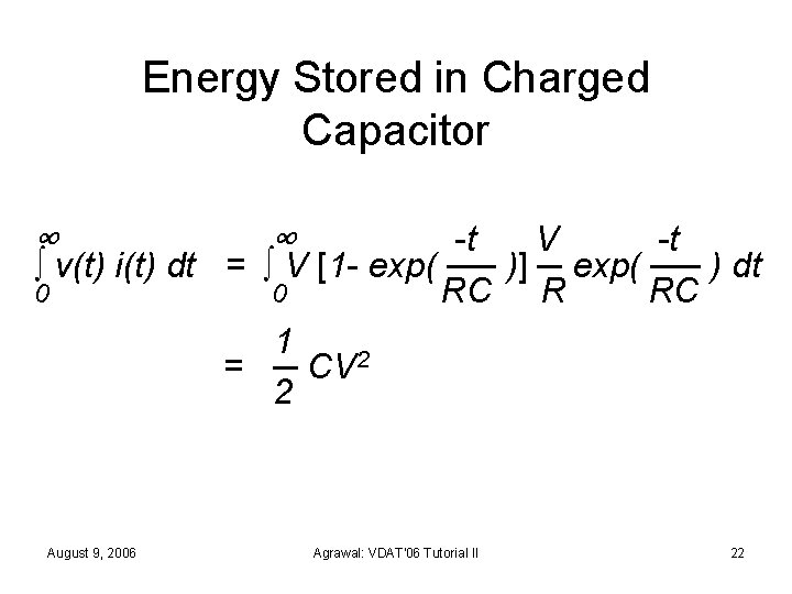
Energy Stored in Charged Capacitor ∞ ∞ -t V -t ∫ v(t) i(t) dt = ∫ V [1 - exp( ── )] ─ exp( ── ) dt 0 0 RC R RC 1 = ─ CV 2 2 August 9, 2006 Agrawal: VDAT'06 Tutorial II 22

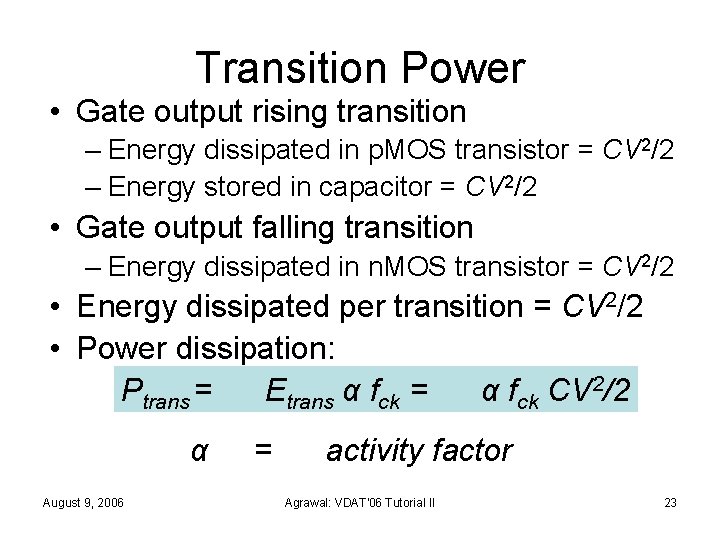
Transition Power • Gate output rising transition – Energy dissipated in p. MOS transistor = CV 2/2 – Energy stored in capacitor = CV 2/2 • Gate output falling transition – Energy dissipated in n. MOS transistor = CV 2/2 • Energy dissipated per transition = CV 2/2 • Power dissipation: Ptrans = Etrans α fck = α fck CV 2/2 α August 9, 2006 = activity factor Agrawal: VDAT'06 Tutorial II 23

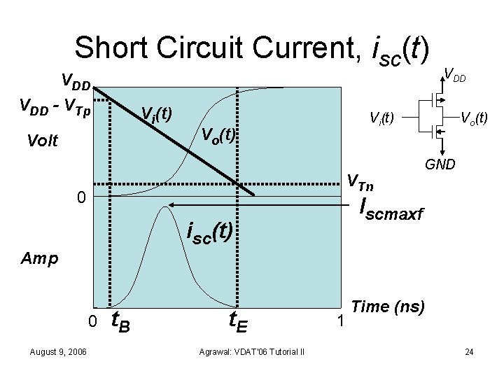
Short Circuit Current, isc(t) VDD - VTp Vi(t) Volt VDD Vi(t) Vo(t) VTn 0 Vo(t) GND Iscmaxf isc(t) Amp 0 August 9, 2006 t. B t. E Agrawal: VDAT'06 Tutorial II 1 Time (ns) 24

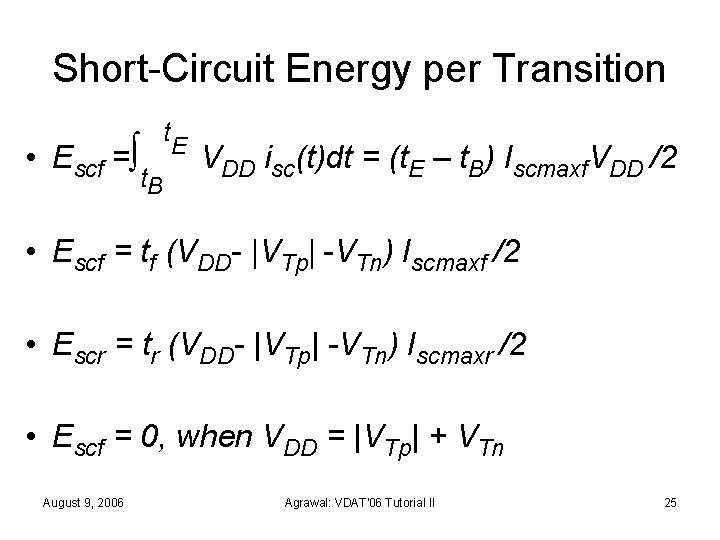
Short-Circuit Energy per Transition • Escf =∫ t. E t. B VDD isc(t)dt = (t. E – t. B) Iscmaxf. VDD /2 • Escf = tf (VDD- |VTp| -VTn) Iscmaxf /2 • Escr = tr (VDD- |VTp| -VTn) Iscmaxr /2 • Escf = 0, when VDD = |VTp| + VTn August 9, 2006 Agrawal: VDAT'06 Tutorial II 25

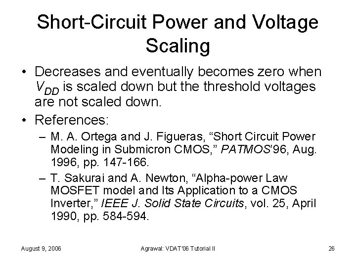
Short-Circuit Power and Voltage Scaling • Decreases and eventually becomes zero when VDD is scaled down but the threshold voltages are not scaled down. • References: – M. A. Ortega and J. Figueras, “Short Circuit Power Modeling in Submicron CMOS, ” PATMOS’ 96, Aug. 1996, pp. 147 -166. – T. Sakurai and A. Newton, “Alpha-power Law MOSFET model and Its Application to a CMOS Inverter, ” IEEE J. Solid State Circuits, vol. 25, April 1990, pp. 584 -594. August 9, 2006 Agrawal: VDAT'06 Tutorial II 26

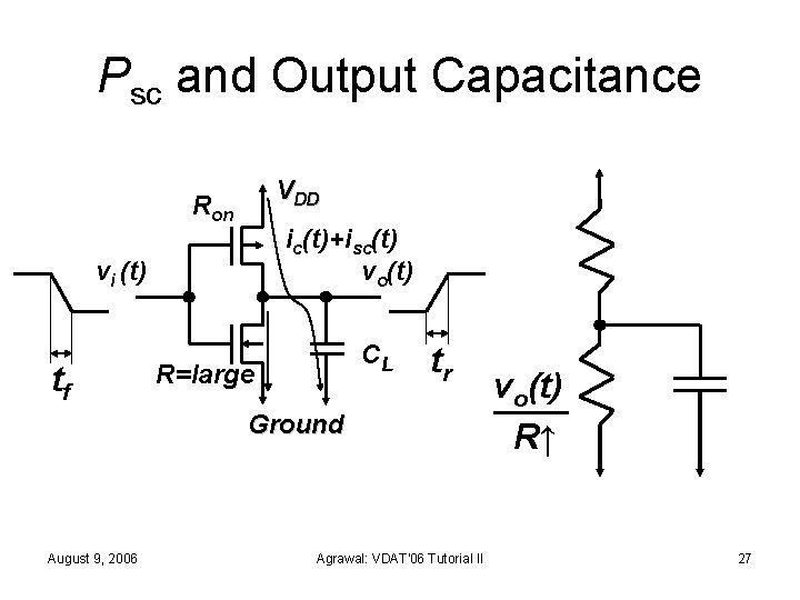
Psc and Output Capacitance VDD Ron ic(t)+isc(t) vo(t) vi (t) tf CL R=large tr Ground August 9, 2006 Agrawal: VDAT'06 Tutorial II vo(t) ─── R↑ 27
![isc and Output Capacitance Isct August 9 2006 t VDD1 exp vot isc and Output Capacitance Isc(t) = August 9, 2006 -t VDD[1 - exp(─────)] vo(t)](https://slidetodoc.com/presentation_image_h/8214a8e0100fbfd18560c29c4ac673be/image-28.jpg)
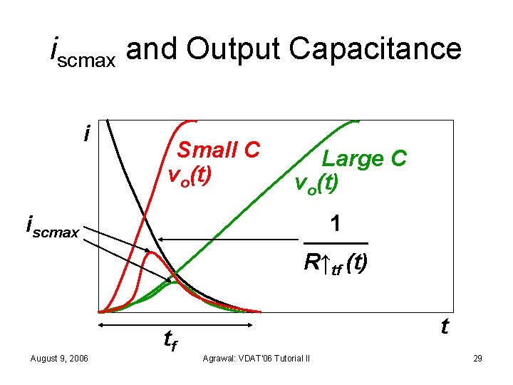
isc and Output Capacitance Isc(t) = August 9, 2006 -t VDD[1 - exp(─────)] vo(t) R↓tf (t)C ──── = ─────── R↑tf (t) Agrawal: VDAT'06 Tutorial II 28

iscmax and Output Capacitance i Small C vo(t) 1 ──── R↑tf (t) iscmax August 9, 2006 Large C vo(t) tf t Agrawal: VDAT'06 Tutorial II 29

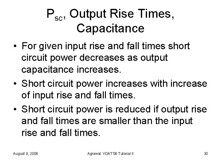
Psc, Output Rise Times, Capacitance • For given input rise and fall times short circuit power decreases as output capacitance increases. • Short circuit power increases with increase of input rise and fall times. • Short circuit power is reduced if output rise and fall times are smaller than the input rise and fall times. August 9, 2006 Agrawal: VDAT'06 Tutorial II 30

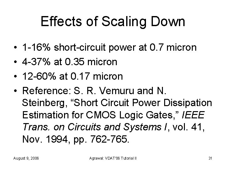
Effects of Scaling Down • • 1 -16% short-circuit power at 0. 7 micron 4 -37% at 0. 35 micron 12 -60% at 0. 17 micron Reference: S. R. Vemuru and N. Steinberg, “Short Circuit Power Dissipation Estimation for CMOS Logic Gates, ” IEEE Trans. on Circuits and Systems I, vol. 41, Nov. 1994, pp. 762 -765. August 9, 2006 Agrawal: VDAT'06 Tutorial II 31

Summary: Short-Circuit Power • Short-circuit power is consumed by each transition (increases with input transition time). • Reduction requires that gate output transition should not be faster than the input transition (faster gates can consume more short-circuit power). • Increasing the output load capacitance reduces short-circuit power. • Scaling down of supply voltage with respect to threshold voltages reduces short-circuit power. August 9, 2006 Agrawal: VDAT'06 Tutorial II 32

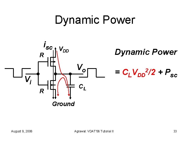
Dynamic Power isc R VDD Dynamic Power Vo Vi = CLVDD 2/2 + Psc CL R Ground August 9, 2006 Agrawal: VDAT'06 Tutorial II 33

Dynamic Power Reduction • Reduce power per transition – Reduced voltage operation – voltage scaling – Capacitance minimization – device sizing • Reduce number of transitions – Glitch elimination August 9, 2006 Agrawal: VDAT'06 Tutorial II 34

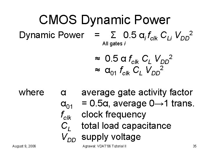
CMOS Dynamic Power = Σ 0. 5 αi fclk CLi VDD 2 All gates i ≈ 0. 5 α fclk CL VDD 2 ≈ α 01 fclk CL VDD 2 where August 9, 2006 α α 01 fclk CL VDD average gate activity factor = 0. 5α, average 0→ 1 trans. clock frequency total load capacitance supply voltage Agrawal: VDAT'06 Tutorial II 35

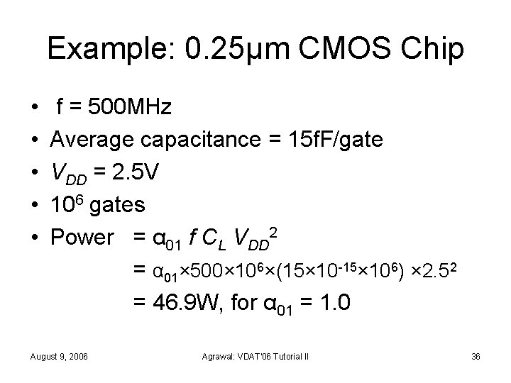
Example: 0. 25μm CMOS Chip • • • f = 500 MHz Average capacitance = 15 f. F/gate VDD = 2. 5 V 106 gates Power = α 01 f CL VDD 2 = α 01× 500× 106×(15× 10 -15× 106) × 2. 52 = 46. 9 W, for α 01 = 1. 0 August 9, 2006 Agrawal: VDAT'06 Tutorial II 36

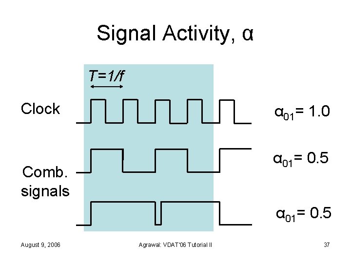
Signal Activity, α T=1/f Clock α 01= 1. 0 α 01= 0. 5 Comb. signals α 01= 0. 5 August 9, 2006 Agrawal: VDAT'06 Tutorial II 37

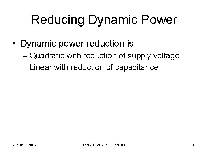
Reducing Dynamic Power • Dynamic power reduction is – Quadratic with reduction of supply voltage – Linear with reduction of capacitance August 9, 2006 Agrawal: VDAT'06 Tutorial II 38

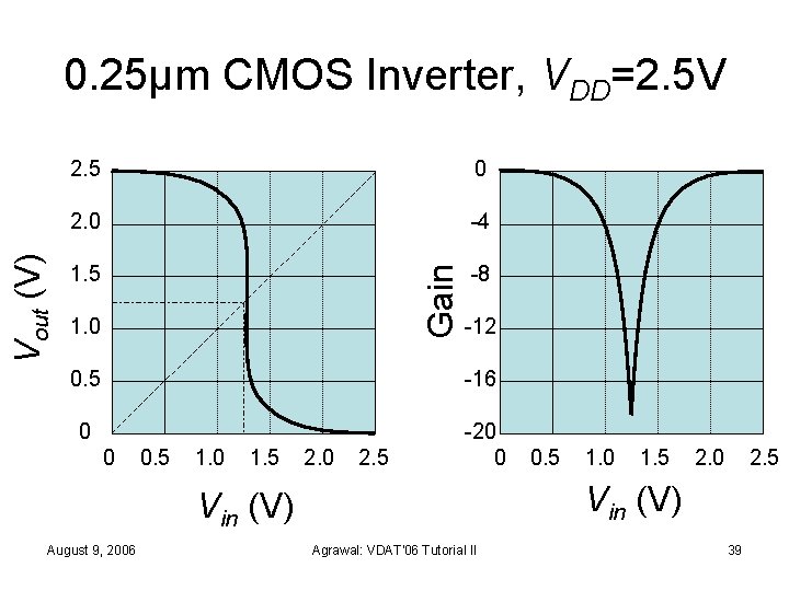
2. 5 0 2. 0 -4 1. 5 -8 Gain Vout (V) 0. 25μm CMOS Inverter, VDD=2. 5 V 1. 0 -12 0. 5 -16 0 -20 0 0 0. 5 1. 0 1. 5 2. 0 2. 5 Vin (V) August 9, 2006 0. 5 Agrawal: VDAT'06 Tutorial II 39

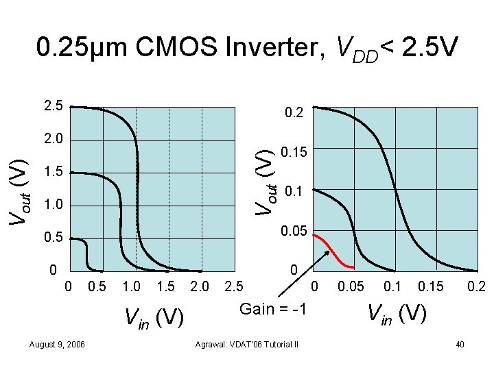
0. 25μm CMOS Inverter, VDD< 2. 5 V 2. 5 0. 2 Vout (V) 2. 0 1. 5 1. 0 0. 15 0. 1 0. 5 0. 05 0 0. 5 1. 0 1. 5 Vin (V) August 9, 2006 2. 0 2. 5 Gain = -1 Agrawal: VDAT'06 Tutorial II 0 0. 05 0. 15 0. 2 Vin (V) 40

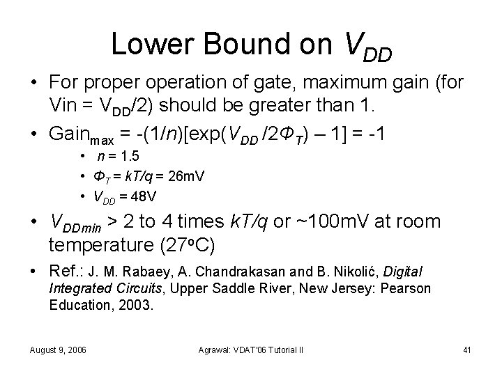
Lower Bound on VDD • For properation of gate, maximum gain (for Vin = VDD/2) should be greater than 1. • Gainmax = -(1/n)[exp(VDD /2ΦT) – 1] = -1 • n = 1. 5 • ΦT = k. T/q = 26 m. V • VDD = 48 V • VDDmin > 2 to 4 times k. T/q or ~100 m. V at room temperature (27 o. C) • Ref. : J. M. Rabaey, A. Chandrakasan and B. Nikolić, Digital Integrated Circuits, Upper Saddle River, New Jersey: Pearson Education, 2003. August 9, 2006 Agrawal: VDAT'06 Tutorial II 41

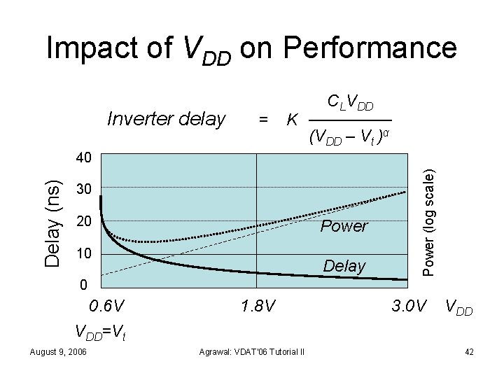
Impact of VDD on Performance Inverter delay = CLVDD K ─────── (VDD – Vt )α 30 20 Power 10 Delay Power (log scale) Delay (ns) 40 0 0. 6 V VDD=Vt August 9, 2006 1. 8 V Agrawal: VDAT'06 Tutorial II 3. 0 V VDD 42

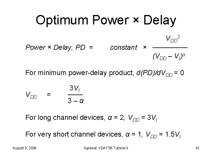
Optimum Power × Delay, PD = VDD 3 constant × ─────── (VDD – Vt)α For minimum power-delay product, d(PD)/d. VDD = 0 VDD = 3 Vt ─── 3–α For long channel devices, α = 2, VDD = 3 Vt For very short channel devices, α = 1, VDD = 1. 5 Vt August 9, 2006 Agrawal: VDAT'06 Tutorial II 43

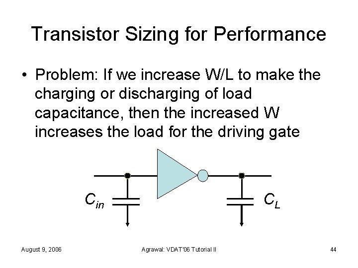
Transistor Sizing for Performance • Problem: If we increase W/L to make the charging or discharging of load capacitance, then the increased W increases the load for the driving gate Cin August 9, 2006 CL Agrawal: VDAT'06 Tutorial II 44

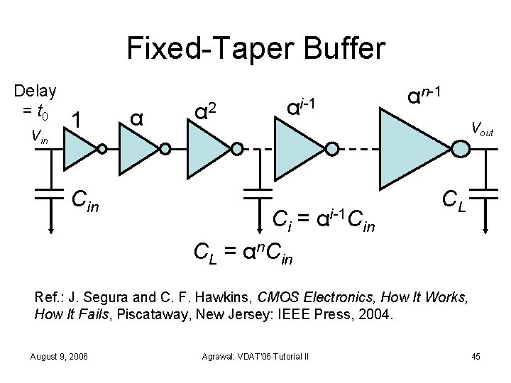
Fixed-Taper Buffer Delay = t 0 Vin 1 Cin α α 2 αi-1 Ci = αi-1 Cin CL = αn. Cin αn-1 Vout CL Ref. : J. Segura and C. F. Hawkins, CMOS Electronics, How It Works, How It Fails, Piscataway, New Jersey: IEEE Press, 2004. August 9, 2006 Agrawal: VDAT'06 Tutorial II 45

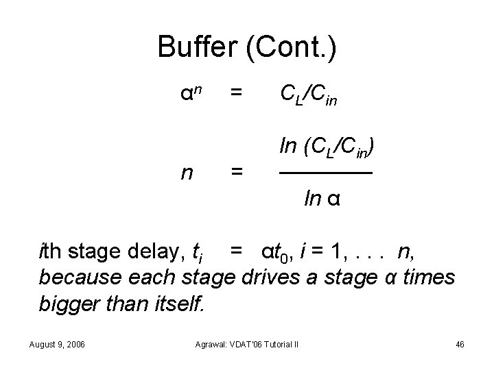
Buffer (Cont. ) αn n = CL/Cin = ln (CL/Cin) ────── ln α ith stage delay, ti = αt 0, i = 1, . . . n, because each stage drives a stage α times bigger than itself. August 9, 2006 Agrawal: VDAT'06 Tutorial II 46

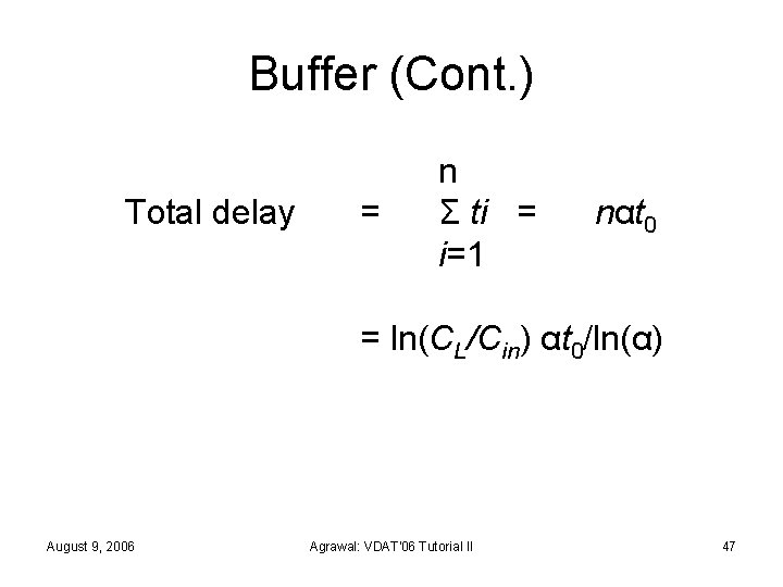
Buffer (Cont. ) Total delay = n Σ ti = i=1 nαt 0 = ln(CL/Cin) αt 0/ln(α) August 9, 2006 Agrawal: VDAT'06 Tutorial II 47

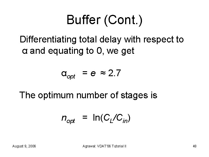
Buffer (Cont. ) Differentiating total delay with respect to α and equating to 0, we get αopt = e ≈ 2. 7 The optimum number of stages is nopt = ln(CL/Cin) August 9, 2006 Agrawal: VDAT'06 Tutorial II 48

Further Reading B. S. Cherkauer and E. G. Friedman, “A Unified Design Methodology for CMOS Tapered Buffers, ” IEEE Trans. VLSI Systems, vol. 3, no. 1, pp. 99 -111, March 1995. August 9, 2006 Agrawal: VDAT'06 Tutorial II 49

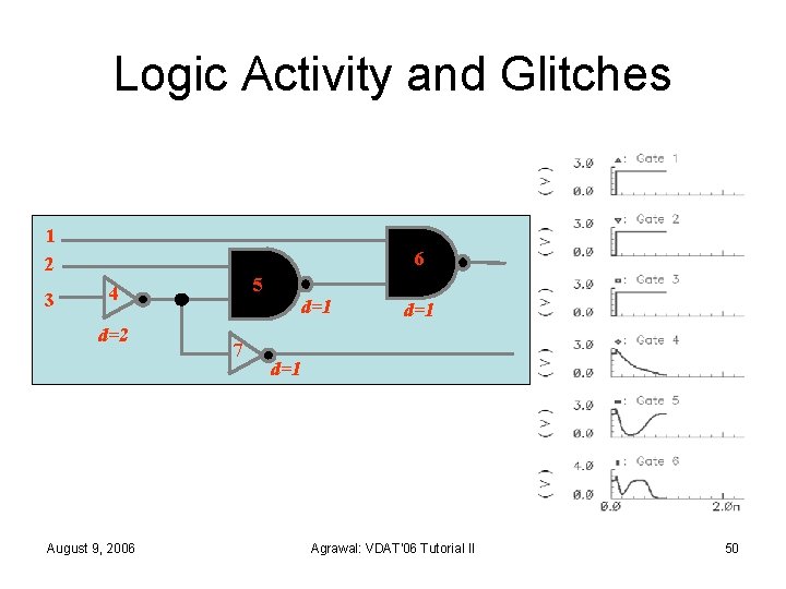
Logic Activity and Glitches 1 2 3 6 5 4 d=2 August 9, 2006 7 d=1 d=1 Agrawal: VDAT'06 Tutorial II 50

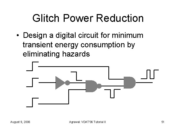
Glitch Power Reduction • Design a digital circuit for minimum transient energy consumption by eliminating hazards August 9, 2006 Agrawal: VDAT'06 Tutorial II 51

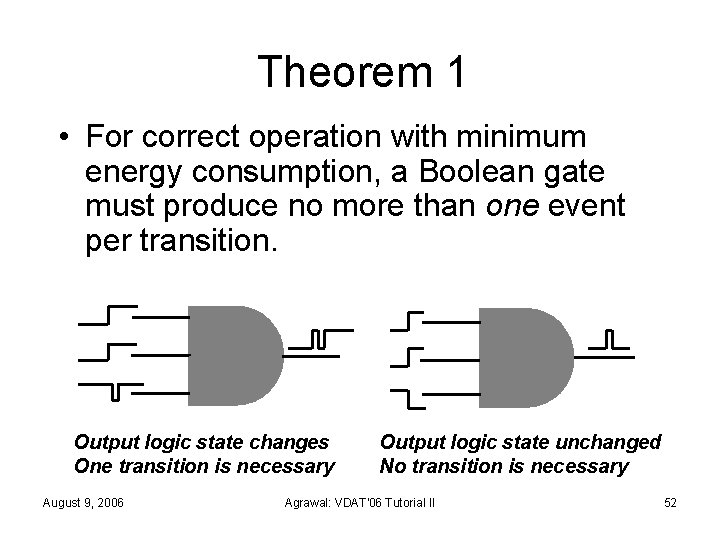
Theorem 1 • For correct operation with minimum energy consumption, a Boolean gate must produce no more than one event per transition. Output logic state changes One transition is necessary August 9, 2006 Output logic state unchanged No transition is necessary Agrawal: VDAT'06 Tutorial II 52

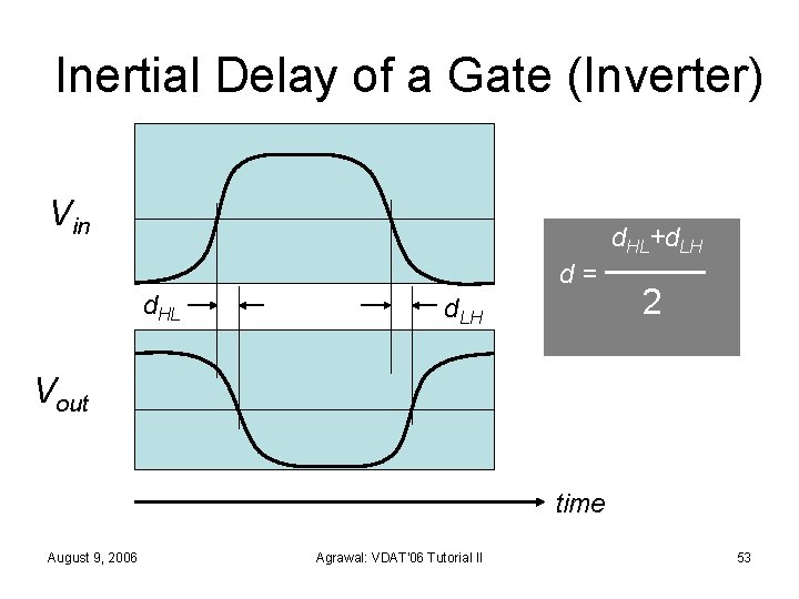
Inertial Delay of a Gate (Inverter) Vin d. HL+d. LH d. HL d = ──── 2 d. LH Vout time August 9, 2006 Agrawal: VDAT'06 Tutorial II 53

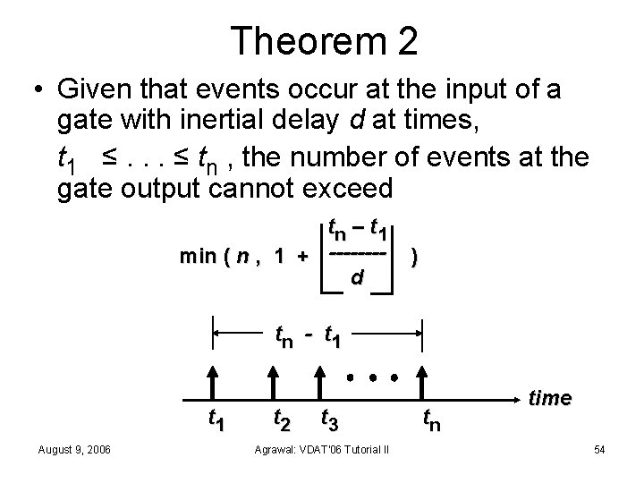
Theorem 2 • Given that events occur at the input of a gate with inertial delay d at times, t 1 ≤. . . ≤ tn , the number of events at the gate output cannot exceed tn – t 1 min ( n , 1 + -------d ) tn - t 1 August 9, 2006 t 2 t 3 Agrawal: VDAT'06 Tutorial II tn time 54

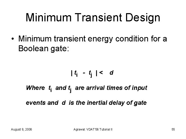
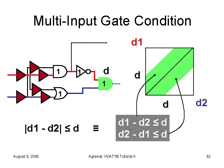
Minimum Transient Design • Minimum transient energy condition for a Boolean gate: | ti - tj | < d Where ti and tj are arrival times of input events and d is the inertial delay of gate August 9, 2006 Agrawal: VDAT'06 Tutorial II 55

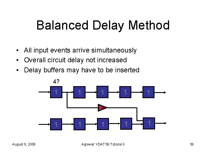
Balanced Delay Method • All input events arrive simultaneously • Overall circuit delay not increased • Delay buffers may have to be inserted 4? 1 1 1 1 3 1 August 9, 2006 1 1 Agrawal: VDAT'06 Tutorial II 56

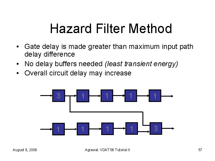
Hazard Filter Method • Gate delay is made greater than maximum input path delay difference • No delay buffers needed (least transient energy) • Overall circuit delay may increase August 9, 2006 3 1 1 1 1 3 Agrawal: VDAT'06 Tutorial II 57

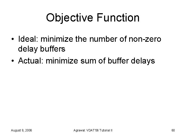
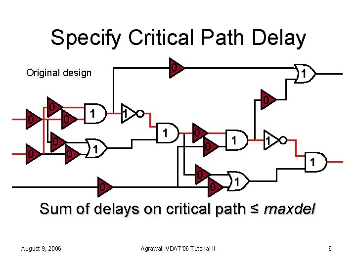
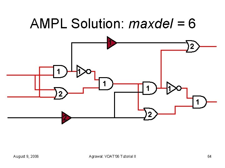
Glitch-Free Design by Linear Programming • • Variables: gate and buffer delays Objective: minimize number of buffers Subject to: overall circuit delay Subject to: minimum transient condition for multi-input gate August 9, 2006 Agrawal: VDAT'06 Tutorial II 58

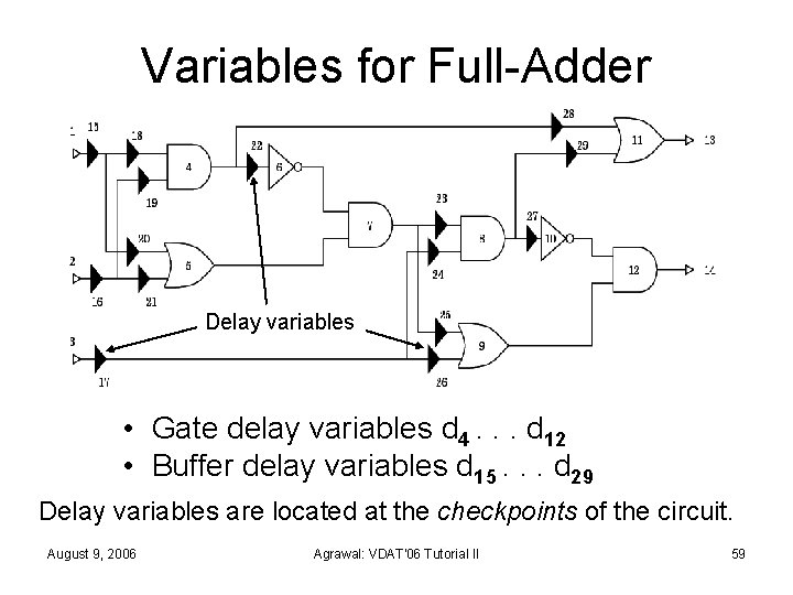
Variables for Full-Adder Delay variables • Gate delay variables d 4. . . d 12 • Buffer delay variables d 15. . . d 29 Delay variables are located at the checkpoints of the circuit. August 9, 2006 Agrawal: VDAT'06 Tutorial II 59

Objective Function • Ideal: minimize the number of non-zero delay buffers • Actual: minimize sum of buffer delays August 9, 2006 Agrawal: VDAT'06 Tutorial II 60

Specify Critical Path Delay 0 Original design 0 0 0 1 0 1 1 1 0 0 0 1 1 1 0 1 Sum of delays on critical path ≤ maxdel August 9, 2006 Agrawal: VDAT'06 Tutorial II 61

Multi-Input Gate Condition d 1 1 d 1 d |d 1 - d 2| ≤ d August 9, 2006 ≡ d 2 d 1 - d 2 ≤ d d 2 - d 1 ≤ d Agrawal: VDAT'06 Tutorial II 62

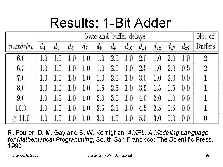
Results: 1 -Bit Adder R. Fourer, D. M. Gay and B. W. Kernighan, AMPL: A Modeling Language for Mathematical Programming, South San Francisco: The Scientific Press, 1993. August 9, 2006 Agrawal: VDAT'06 Tutorial II 63

AMPL Solution: maxdel = 6 1 1 2 1 1 1 2 2 August 9, 2006 2 Agrawal: VDAT'06 Tutorial II 64

AMPL Solution: maxdel = 7 3 1 1 1 2 1 2 August 9, 2006 1 Agrawal: VDAT'06 Tutorial II 65

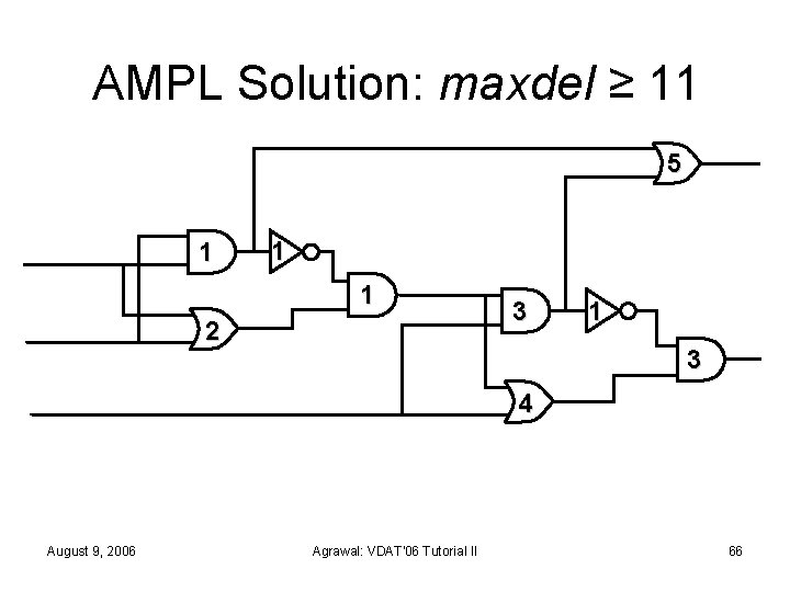
AMPL Solution: maxdel ≥ 11 5 1 1 1 2 3 1 3 4 August 9, 2006 Agrawal: VDAT'06 Tutorial II 66

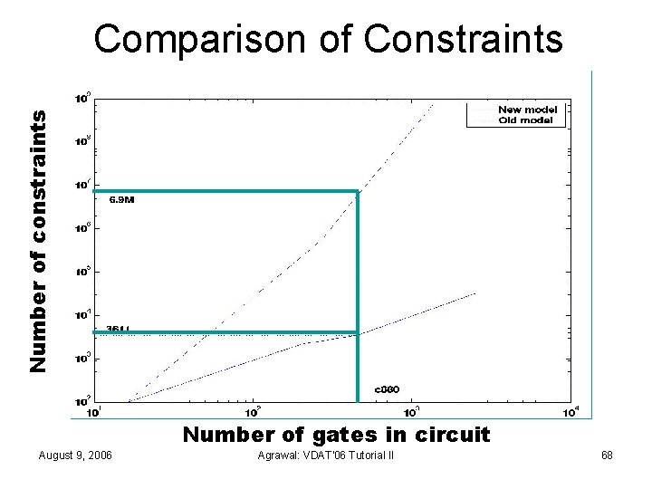
Removing a Limitation • Constraints are written by path enumeration. • Since number of paths in a circuit can be exponential in circuit size, the formulation is infeasible for large circuits. • Example: c 880 has 6. 96 M constraints. • Solution: A linear complexity method. See, – T. Raja, Master’s Thesis, Rutgers University, 2002. – T. Raja, V. D. Agrawal and M. L. Bushnell, “Minimum Dynamic Power CMOS Circuit Design by a Reduced Constraint Set Linear Program, ” Proc. 16 th International Conf. VLSI Design, 2003, pp. 527 -532. August 9, 2006 Agrawal: VDAT'06 Tutorial II 67

Number of constraints Comparison of Constraints Number of gates in circuit August 9, 2006 Agrawal: VDAT'06 Tutorial II 68

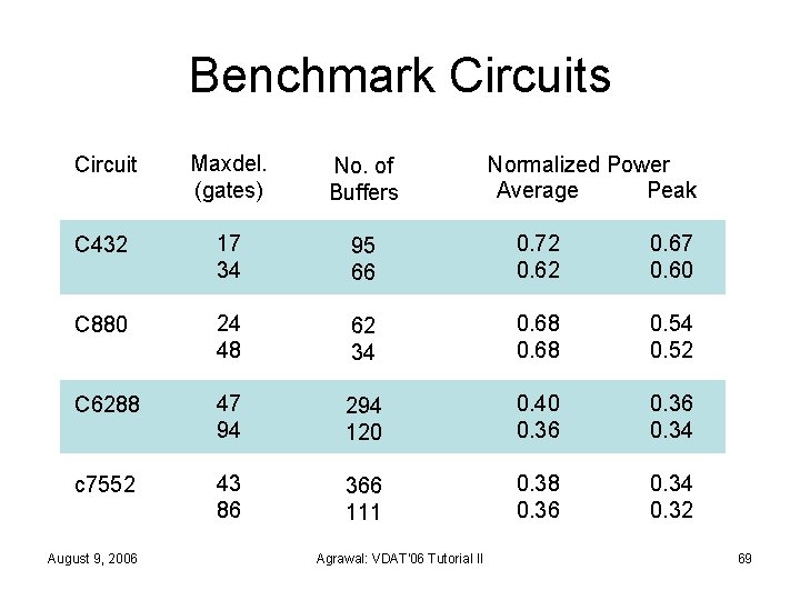
Benchmark Circuits Circuit Maxdel. (gates) No. of Buffers C 432 17 34 95 66 0. 72 0. 67 0. 60 C 880 24 48 62 34 0. 68 0. 54 0. 52 C 6288 47 94 294 120 0. 40 0. 36 0. 34 c 7552 43 86 366 111 0. 38 0. 36 0. 34 0. 32 August 9, 2006 Agrawal: VDAT'06 Tutorial II Normalized Power Average Peak 69

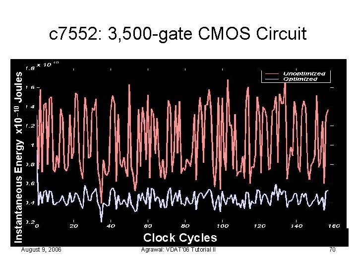
Instantaneous Energy x 10 --10 Joules c 7552: 3, 500 -gate CMOS Circuit August 9, 2006 Clock Cycles Agrawal: VDAT'06 Tutorial II 70

References • • R. Fourer, D. M. Gay and B. W. Kernighan, AMPL: A Modeling Language for Mathematical Programming, South San Francisco: The Scientific Press, 1993. M. Berkelaar and E. Jacobs, “Using Gate Sizing to Reduce Glitch Power, ” Proc. Pro. RISC Workshop, Mierlo, The Netherlands, Nov. 1996, pp. 183 -188. V. D. Agrawal, “Low Power Design by Hazard Filtering, ” Proc. 10 th Int’l Conf. VLSI Design, Jan. 1997, pp. 193 -197. V. D. Agrawal, M. L. Bushnell, G. Parthasarathy and R. Ramadoss, “Digital Circuit Design for Minimum Transient Energy and Linear Programming Method, ” Proc. 12 th Int’l Conf. VLSI Design, Jan. 1999, pp. 434 -439. M. Hsiao, E. M. Rudnick and J. H. Patel, “Effects of Delay Model in Peak Power Estimation of VLSI Circuits, ” Proc. ICCAD, Nov. 1997, pp. 45 -51. T. Raja, A Reduced Constraint Set Linear Program for Low Power Design of Digital Circuits, Master’s Thesis, Rutgers Univ. , New Jersey, 2002. T. Raja, V. D. Agrawal and M. L. Bushnell, “Transistor Sizing of Logic gates to Maximize Input Delay Variability, ” J. of Low Power Electronics (JOLPE), vol. 2, pp. 121 -128, 2006. August 9, 2006 Agrawal: VDAT'06 Tutorial II 71

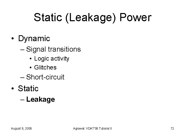
Static (Leakage) Power • Dynamic – Signal transitions • Logic activity • Glitches – Short-circuit • Static – Leakage August 9, 2006 Agrawal: VDAT'06 Tutorial II 72

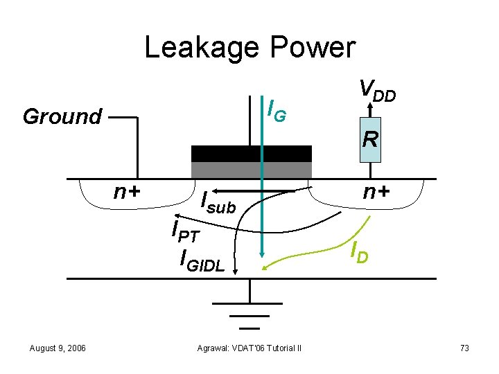
Leakage Power IG Ground R n+ Isub IPT IGIDL August 9, 2006 VDD Agrawal: VDAT'06 Tutorial II n+ ID 73

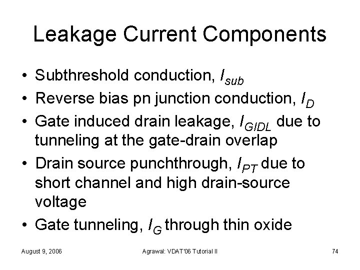
Leakage Current Components • Subthreshold conduction, Isub • Reverse bias pn junction conduction, ID • Gate induced drain leakage, IGIDL due to tunneling at the gate-drain overlap • Drain source punchthrough, IPT due to short channel and high drain-source voltage • Gate tunneling, IG through thin oxide August 9, 2006 Agrawal: VDAT'06 Tutorial II 74

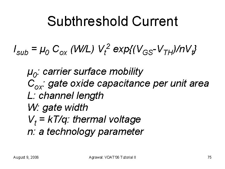
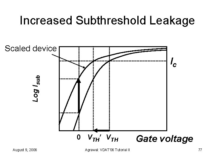
Subthreshold Current Isub = μ 0 Cox (W/L) Vt 2 exp{(VGS-VTH)/n. Vt} μ 0: carrier surface mobility Cox: gate oxide capacitance per unit area L: channel length W: gate width Vt = k. T/q: thermal voltage n: a technology parameter August 9, 2006 Agrawal: VDAT'06 Tutorial II 75

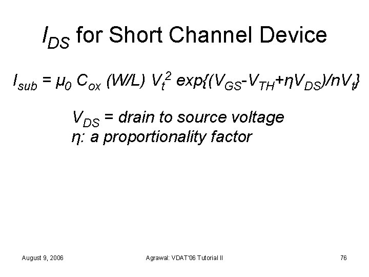
IDS for Short Channel Device Isub = μ 0 Cox (W/L) Vt 2 exp{(VGS-VTH+ηVDS)/n. Vt} VDS = drain to source voltage η: a proportionality factor August 9, 2006 Agrawal: VDAT'06 Tutorial II 76

Increased Subthreshold Leakage Scaled device Log Isub Ic 0 VTH’ VTH August 9, 2006 Agrawal: VDAT'06 Tutorial II Gate voltage 77

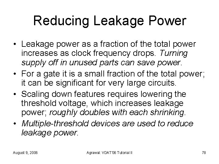
Reducing Leakage Power • Leakage power as a fraction of the total power increases as clock frequency drops. Turning supply off in unused parts can save power. • For a gate it is a small fraction of the total power; it can be significant for very large circuits. • Scaling down features requires lowering the threshold voltage, which increases leakage power; roughly doubles with each shrinking. • Multiple-threshold devices are used to reduce leakage power. August 9, 2006 Agrawal: VDAT'06 Tutorial II 78

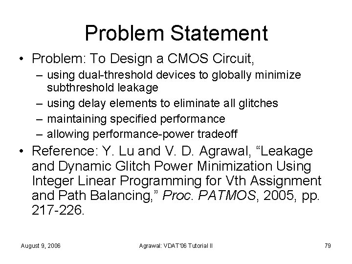
Problem Statement • Problem: To Design a CMOS Circuit, – using dual-threshold devices to globally minimize subthreshold leakage – using delay elements to eliminate all glitches – maintaining specified performance – allowing performance-power tradeoff • Reference: Y. Lu and V. D. Agrawal, “Leakage and Dynamic Glitch Power Minimization Using Integer Linear Programming for Vth Assignment and Path Balancing, ” Proc. PATMOS, 2005, pp. 217 -226. August 9, 2006 Agrawal: VDAT'06 Tutorial II 79

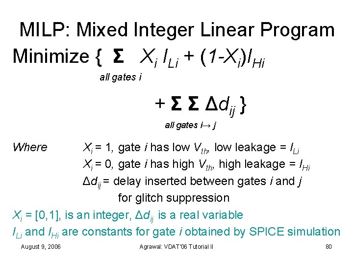
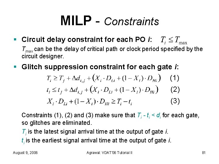
MILP: Mixed Integer Linear Program Minimize { Σ Xi ILi + (1 -Xi)IHi all gates i + Σ Σ Δdij } all gates i→ j Where Xi = 1, gate i has low Vth, low leakage = ILi Xi = 0, gate i has high Vth, high leakage = IHi Δdij = delay inserted between gates i and j for glitch suppression Xi = [0, 1], is an integer, Δdij is a real variable ILi and IHi are constants for gate i obtained by SPICE simulation August 9, 2006 Agrawal: VDAT'06 Tutorial II 80

MILP - Constraints § Circuit delay constraint for each PO i: Tmax can be the delay of critical path or clock period specified by the circuit designer. § Glitch suppression constraint for each gate i: (1) (2) (3) Constraints (1), (2) and (3) make sure that Ti - ti < di for each gate, so glitches are eliminated. Ti is the latest signal arrival time at the output of gate i. ti is the earliest signal arrival time at the output of gate i. August 9, 2006 Agrawal: VDAT'06 Tutorial II 81

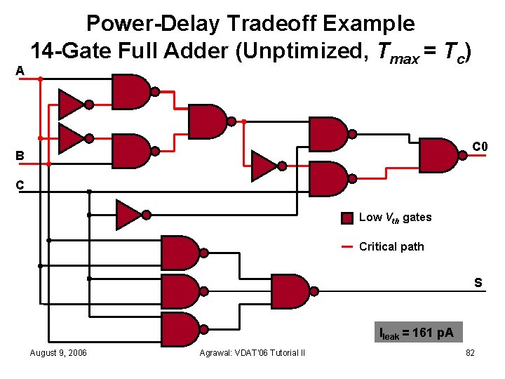
A Power-Delay Tradeoff Example 14 -Gate Full Adder (Unptimized, Tmax = Tc) C 0 B C Low Vth gates Critical path S Ileak = 161 p. A August 9, 2006 Agrawal: VDAT'06 Tutorial II 82

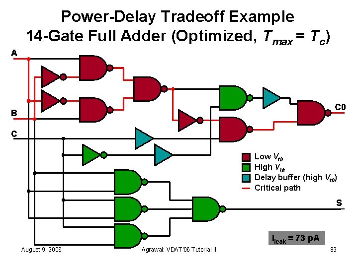
Power-Delay Tradeoff Example 14 -Gate Full Adder (Optimized, Tmax = Tc) A C 0 B C Low Vth High Vth Delay buffer (high Vth) Critical path S Ileak = 73 p. A August 9, 2006 Agrawal: VDAT'06 Tutorial II 83

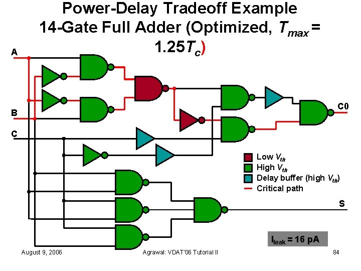
A Power-Delay Tradeoff Example 14 -Gate Full Adder (Optimized, Tmax = 1. 25 Tc) C 0 B C Low Vth High Vth Delay buffer (high Vth) Critical path S Ileak = 16 p. A August 9, 2006 Agrawal: VDAT'06 Tutorial II 84

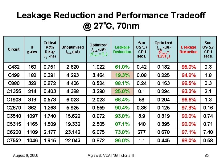
Leakage Reduction and Performance Tradeoff @ 27℃, 70 nm Circuit # gates Critical Path Delay Tc (ns) C 432 160 0. 751 2. 620 1. 022 61. 0% 0. 42 0. 132 95. 0% 0. 3 C 499 182 0. 391 4. 293 3. 464 19. 3% 0. 08 0. 225 94. 8% 1. 8 C 880 328 0. 672 4. 406 0. 524 88. 1% 0. 24 0. 153 96. 5% 0. 3 C 1355 214 0. 403 4. 388 3. 290 25. 0% 0. 1 0. 294 93. 3% 2. 1 C 1908 319 0. 573 6. 023 2. 023 66. 4% 59 0. 204 96. 6% 1. 3 C 2670 362 1. 263 5. 925 0. 659 90. 4% 0. 38 0. 125 97. 9% 0. 16 C 3540 1097 1. 748 15. 622 0. 972 93. 8% 3. 9 0. 319 98. 0% 0. 74 C 5315 1165 1. 589 19. 332 2. 505 87. 1% 140 0. 395 98. 0% 0. 71 C 6288 1189 2. 177 23. 142 6. 075 73. 8% 277 0. 678 97. 1% 7. 48 C 7552 1046 1. 915 22. 043 0. 872 96. 0% 1. 1 0. 445 98. 0% 0. 58 August 9, 2006 Unoptimized Ileak (μA) Optimized Ileak (μA) (Tmax= Tc ) Leakage Reduction Sun OS 5. 7 CPU secs. Optimized Ileak (μA) (Tmax= 1. 25 Tc ) Leakage Reduction Sun OS 5. 7 CPU secs. Agrawal: VDAT'06 Tutorial II 85

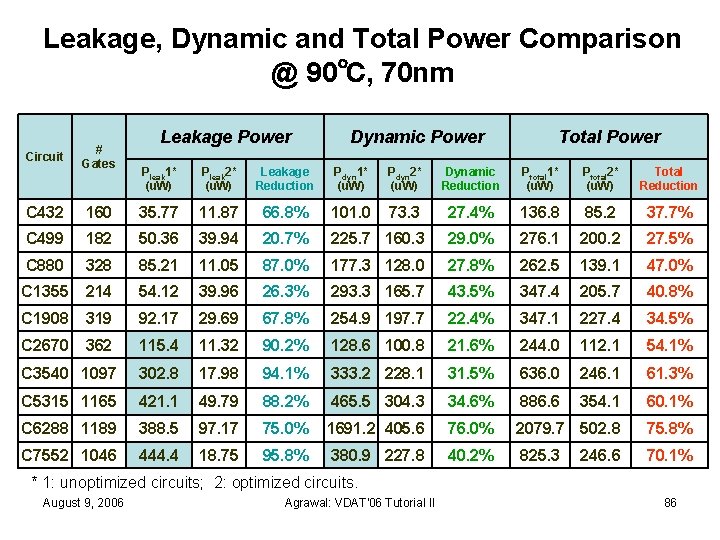
Leakage, Dynamic and Total Power Comparison @ 90℃, 70 nm Circuit # Gates Leakage Power Dynamic Power Total Power Pleak 1* (u. W) Pleak 2* (u. W) Leakage Reduction Pdyn 1* (u. W) Pdyn 2* (u. W) Dynamic Reduction Ptotal 1* (u. W) Ptotal 2* (u. W) Total Reduction C 432 160 35. 77 11. 87 66. 8% 101. 0 73. 3 27. 4% 136. 8 85. 2 37. 7% C 499 182 50. 36 39. 94 20. 7% 225. 7 160. 3 29. 0% 276. 1 200. 2 27. 5% C 880 328 85. 21 11. 05 87. 0% 177. 3 128. 0 27. 8% 262. 5 139. 1 47. 0% C 1355 214 54. 12 39. 96 26. 3% 293. 3 165. 7 43. 5% 347. 4 205. 7 40. 8% C 1908 319 92. 17 29. 69 67. 8% 254. 9 197. 7 22. 4% 347. 1 227. 4 34. 5% C 2670 362 115. 4 11. 32 90. 2% 128. 6 100. 8 21. 6% 244. 0 112. 1 54. 1% C 3540 1097 302. 8 17. 98 94. 1% 333. 2 228. 1 31. 5% 636. 0 246. 1 61. 3% C 5315 1165 421. 1 49. 79 88. 2% 465. 5 304. 3 34. 6% 886. 6 354. 1 60. 1% C 6288 1189 388. 5 97. 17 75. 0% 1691. 2 405. 6 76. 0% 2079. 7 502. 8 75. 8% C 7552 1046 444. 4 18. 75 95. 8% 380. 9 227. 8 40. 2% 825. 3 70. 1% 246. 6 * 1: unoptimized circuits; 2: optimized circuits. August 9, 2006 Agrawal: VDAT'06 Tutorial II 86

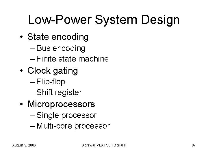
Low-Power System Design • State encoding – Bus encoding – Finite state machine • Clock gating – Flip-flop – Shift register • Microprocessors – Single processor – Multi-core processor August 9, 2006 Agrawal: VDAT'06 Tutorial II 87

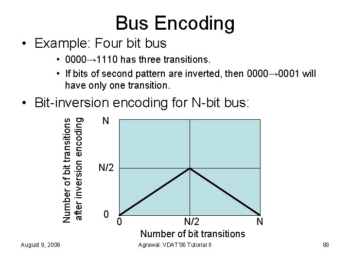
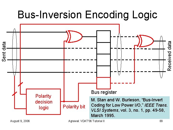
Bus Encoding • Example: Four bit bus • 0000→ 1110 has three transitions. • If bits of second pattern are inverted, then 0000→ 0001 will have only one transition. Number of bit transitions after inversion encoding • Bit-inversion encoding for N-bit bus: August 9, 2006 N N/2 0 0 N/2 Number of bit transitions Agrawal: VDAT'06 Tutorial II N 88

Sent data Received data Bus-Inversion Encoding Logic Polarity decision logic August 9, 2006 Bus register Polarity bit M. Stan and W. Burleson, “Bus-Invert Coding for Low Power I/O, ” IEEE Trans. VLSI Systems, vol. 3, no. 1, pp. 49 -58, March 1995. Agrawal: VDAT'06 Tutorial II 89

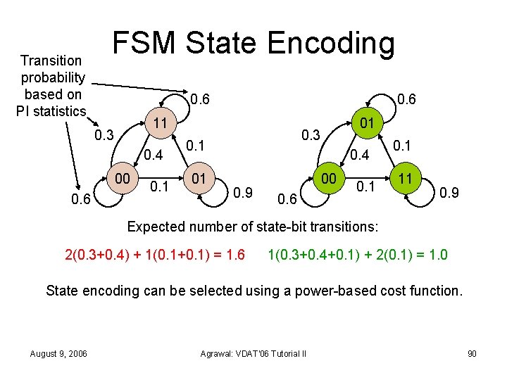
Transition probability based on PI statistics FSM State Encoding 0. 6 11 0. 3 0. 4 00 0. 6 0. 1 0. 3 0. 1 01 01 0. 4 0. 9 00 0. 6 0. 1 11 0. 9 Expected number of state-bit transitions: 2(0. 3+0. 4) + 1(0. 1+0. 1) = 1. 6 1(0. 3+0. 4+0. 1) + 2(0. 1) = 1. 0 State encoding can be selected using a power-based cost function. August 9, 2006 Agrawal: VDAT'06 Tutorial II 90

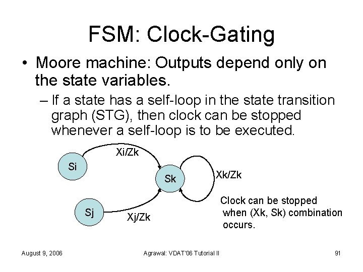
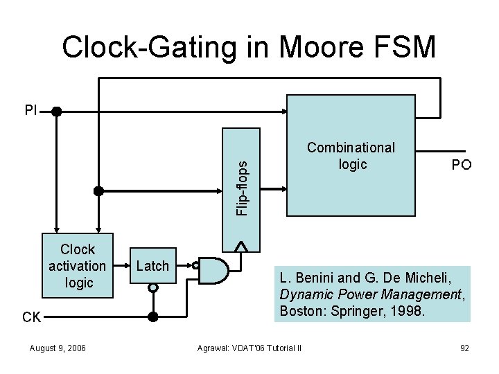
FSM: Clock-Gating • Moore machine: Outputs depend only on the state variables. – If a state has a self-loop in the state transition graph (STG), then clock can be stopped whenever a self-loop is to be executed. Xi/Zk Si Sk Sj August 9, 2006 Xk/Zk Xj/Zk Agrawal: VDAT'06 Tutorial II Clock can be stopped when (Xk, Sk) combination occurs. 91

Clock-Gating in Moore FSM PI Flip-flops Combinational logic Clock activation logic CK August 9, 2006 Latch PO L. Benini and G. De Micheli, Dynamic Power Management, Boston: Springer, 1998. Agrawal: VDAT'06 Tutorial II 92

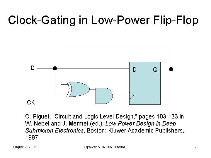
Clock-Gating in Low-Power Flip-Flop D D Q CK C. Piguet, “Circuit and Logic Level Design, ” pages 103 -133 in W. Nebel and J. Mermet (ed. ), Low Power Design in Deep Submicron Electronics, Boston: Kluwer Academic Publishers, 1997. August 9, 2006 Agrawal: VDAT'06 Tutorial II 93

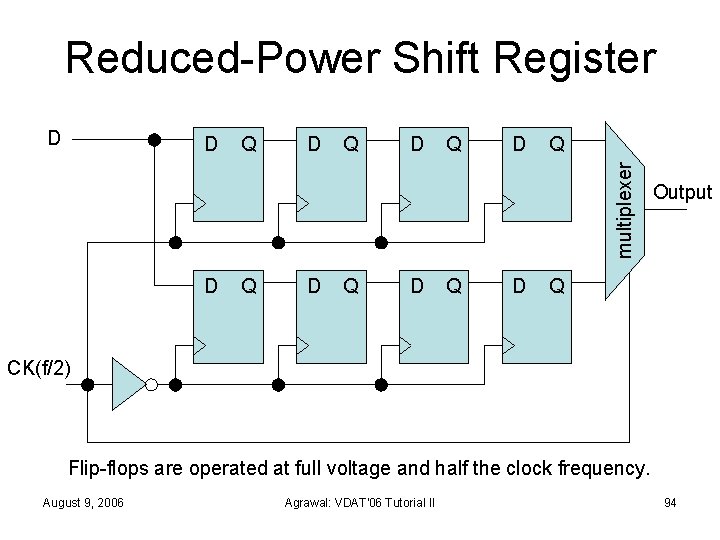
Reduced-Power Shift Register D Q D Q multiplexer D D Q D Q D Output Q CK(f/2) Flip-flops are operated at full voltage and half the clock frequency. August 9, 2006 Agrawal: VDAT'06 Tutorial II 94

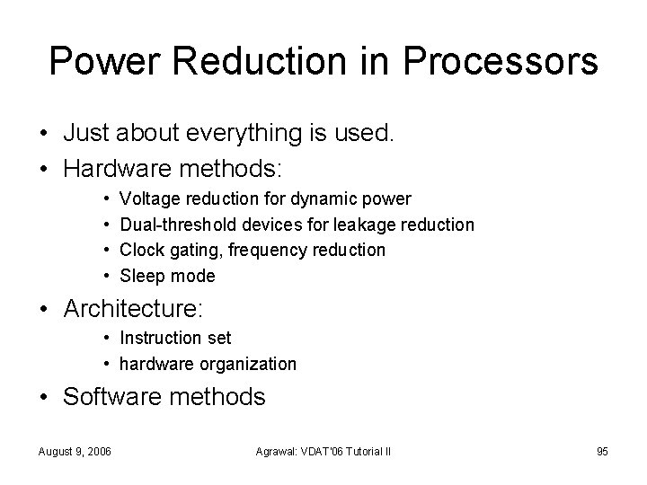
Power Reduction in Processors • Just about everything is used. • Hardware methods: • • Voltage reduction for dynamic power Dual-threshold devices for leakage reduction Clock gating, frequency reduction Sleep mode • Architecture: • Instruction set • hardware organization • Software methods August 9, 2006 Agrawal: VDAT'06 Tutorial II 95

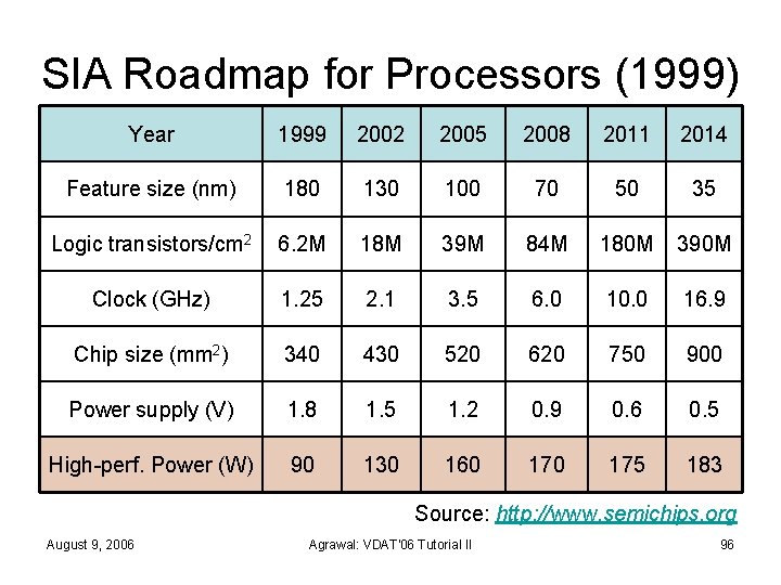
SIA Roadmap for Processors (1999) Year 1999 2002 2005 2008 2011 2014 Feature size (nm) 180 130 100 70 50 35 Logic transistors/cm 2 6. 2 M 18 M 39 M 84 M 180 M 390 M Clock (GHz) 1. 25 2. 1 3. 5 6. 0 10. 0 16. 9 Chip size (mm 2) 340 430 520 620 750 900 Power supply (V) 1. 8 1. 5 1. 2 0. 9 0. 6 0. 5 High-perf. Power (W) 90 130 160 175 183 Source: http: //www. semichips. org August 9, 2006 Agrawal: VDAT'06 Tutorial II 96

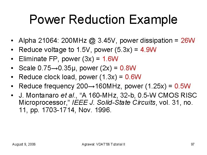
Power Reduction Example • • Alpha 21064: 200 MHz @ 3. 45 V, power dissipation = 26 W Reduce voltage to 1. 5 V, power (5. 3 x) = 4. 9 W Eliminate FP, power (3 x) = 1. 6 W Scale 0. 75→ 0. 35μ, power (2 x) = 0. 8 W Reduce clock load, power (1. 3 x) = 0. 6 W Reduce frequency 200→ 160 MHz, power (1. 25 x) = 0. 5 W J. Montanaro et al. , “A 160 -MHz, 32 -b, 0. 5 -W CMOS RISC Microprocessor, ” IEEE J. Solid-State Circuits, vol. 31, no. 11, pp. 1703 -1714, Nov. 1996. August 9, 2006 Agrawal: VDAT'06 Tutorial II 97

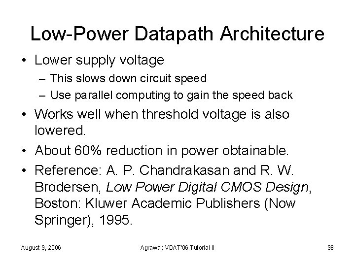
Low-Power Datapath Architecture • Lower supply voltage – This slows down circuit speed – Use parallel computing to gain the speed back • Works well when threshold voltage is also lowered. • About 60% reduction in power obtainable. • Reference: A. P. Chandrakasan and R. W. Brodersen, Low Power Digital CMOS Design, Boston: Kluwer Academic Publishers (Now Springer), 1995. August 9, 2006 Agrawal: VDAT'06 Tutorial II 98

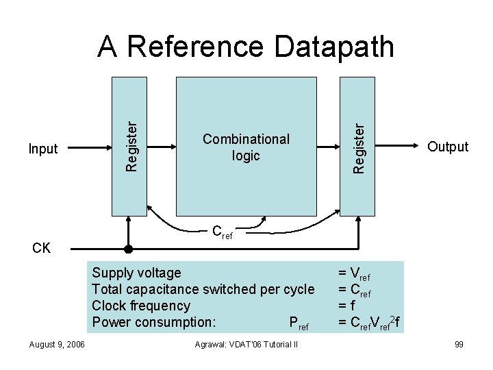
CK Combinational logic Output Cref Supply voltage Total capacitance switched per cycle Clock frequency Power consumption: Pref August 9, 2006 Register Input Register A Reference Datapath Agrawal: VDAT'06 Tutorial II = Vref = Cref =f = Cref. Vref 2 f 99

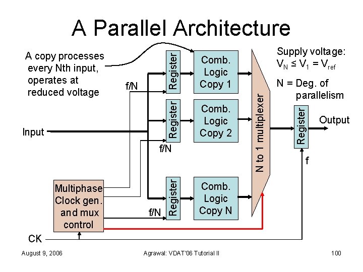
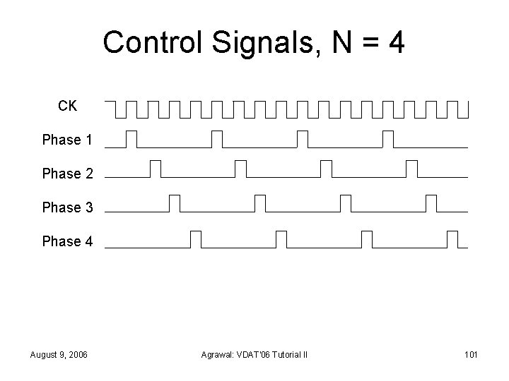
Comb. Logic Copy 2 Multiphase Clock gen. and mux control f/N Register f/N N = Deg. of parallelism Register Input Comb. Logic Copy 1 Supply voltage: VN ≤ V 1 = Vref N to 1 multiplexer f/N Register A copy processes every Nth input, operates at reduced voltage Register A Parallel Architecture Output f Comb. Logic Copy N CK August 9, 2006 Agrawal: VDAT'06 Tutorial II 100

Control Signals, N = 4 CK Phase 1 Phase 2 Phase 3 Phase 4 August 9, 2006 Agrawal: VDAT'06 Tutorial II 101

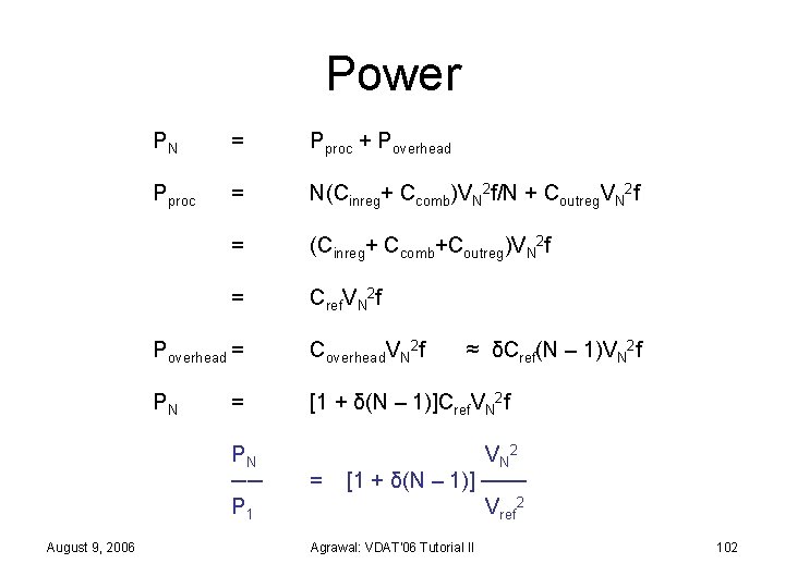
Power PN = Pproc + Poverhead Pproc = N(Cinreg+ Ccomb)VN 2 f/N + Coutreg. VN 2 f = (Cinreg+ Ccomb+Coutreg)VN 2 f = Cref. VN 2 f Poverhead = Coverhead. VN 2 f PN [1 + δ(N – 1)]Cref. VN 2 f = PN ── P 1 August 9, 2006 = ≈ δCref(N – 1)VN 2 f VN 2 [1 + δ(N – 1)] ─── Vref 2 Agrawal: VDAT'06 Tutorial II 102

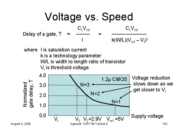
Voltage vs. Speed Delay of a gate, T ≈ CLVref ──── I CLVref ───── k(W/L)(Vref – Vt)2 = where I is saturation current k is a technology parameter W/L is width to length ratio of transistor Vt is threshold voltage Normalized gate delay, T 4. 0 N=2 2. 0 N=1 1. 0 0. 0 August 9, 2006 N=3 3. 0 1. 2μ CMOS Voltage reduction slows down as we get closer to Vt Vt V 3 V 2=2. 9 V Vref =5 V Agrawal: VDAT'06 Tutorial II Supply voltage 103

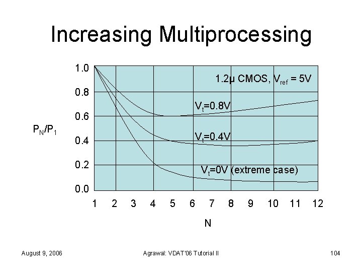
Increasing Multiprocessing 1. 0 1. 2μ CMOS, Vref = 5 V 0. 8 Vt=0. 8 V 0. 6 PN/P 1 Vt=0. 4 V 0. 4 0. 2 Vt=0 V (extreme case) 0. 0 1 2 3 4 5 6 7 8 9 10 11 12 N August 9, 2006 Agrawal: VDAT'06 Tutorial II 104

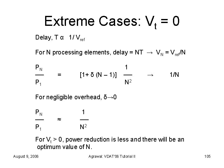
Extreme Cases: Vt = 0 Delay, T α 1/ Vref For N processing elements, delay = NT → VN = Vref/N PN ── P 1 = [1+ δ (N – 1)] 1 ── N 2 → 1/N For negligible overhead, δ→ 0 PN ── P 1 ≈ 1 ── N 2 For Vt > 0, power reduction is less and there will be an optimum value of N. August 9, 2006 Agrawal: VDAT'06 Tutorial II 105

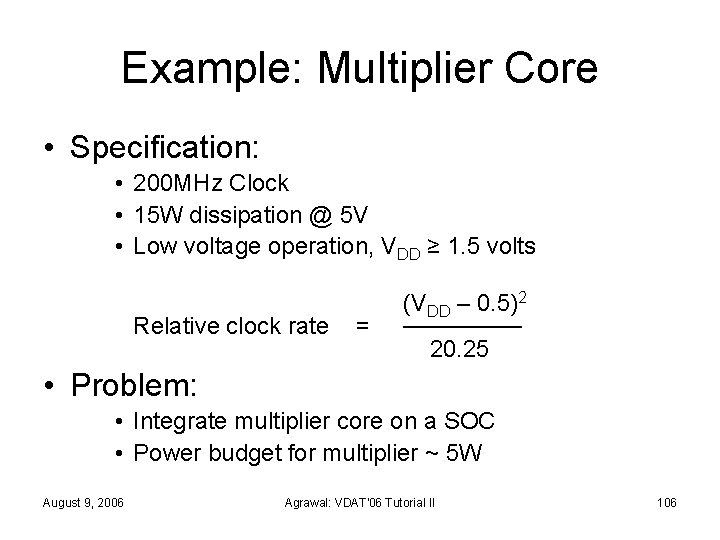
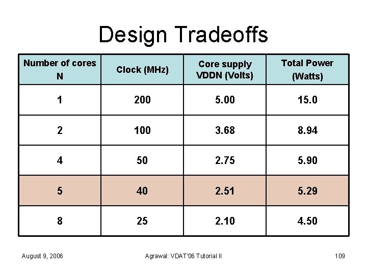
Example: Multiplier Core • Specification: • 200 MHz Clock • 15 W dissipation @ 5 V • Low voltage operation, VDD ≥ 1. 5 volts Relative clock rate = (VDD – 0. 5)2 ─────── 20. 25 • Problem: • Integrate multiplier core on a SOC • Power budget for multiplier ~ 5 W August 9, 2006 Agrawal: VDAT'06 Tutorial II 106

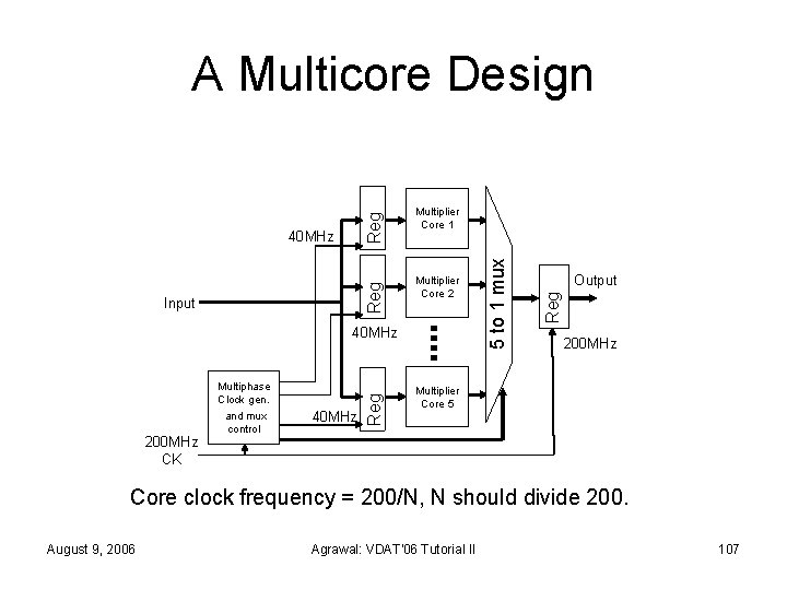
Input Multiplier Core 2 200 MHz CK Multiphase Clock gen. and mux control 40 MHz Reg 40 MHz Output Reg 40 MHz Multiplier Core 1 5 to 1 mux Reg A Multicore Design 200 MHz Multiplier Core 5 Core clock frequency = 200/N, N should divide 200. August 9, 2006 Agrawal: VDAT'06 Tutorial II 107

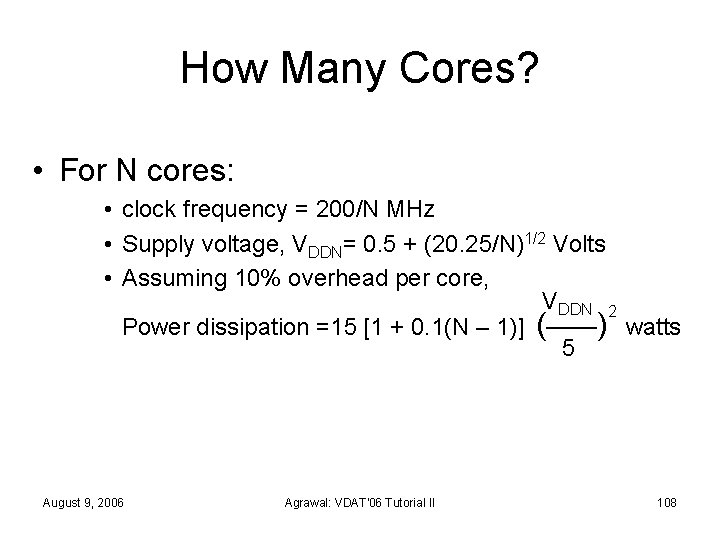
How Many Cores? • For N cores: • clock frequency = 200/N MHz • Supply voltage, VDDN= 0. 5 + (20. 25/N)1/2 Volts • Assuming 10% overhead per core, VDDN 2 Power dissipation =15 [1 + 0. 1(N – 1)] (───) watts 5 August 9, 2006 Agrawal: VDAT'06 Tutorial II 108

Design Tradeoffs Number of cores N Clock (MHz) Core supply VDDN (Volts) Total Power (Watts) 1 200 5. 00 15. 0 2 100 3. 68 8. 94 4 50 2. 75 5. 90 5 40 2. 51 5. 29 8 25 2. 10 4. 50 August 9, 2006 Agrawal: VDAT'06 Tutorial II 109

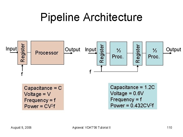
Output Input ½ Proc. Register Processor Register Input Register Pipeline Architecture ½ Proc. Output f f Capacitance = C Voltage = V Frequency = f Power = CV 2 f August 9, 2006 Capacitance = 1. 2 C Voltage = 0. 6 V Frequency = f Power = 0. 432 CV 2 f Agrawal: VDAT'06 Tutorial II 110

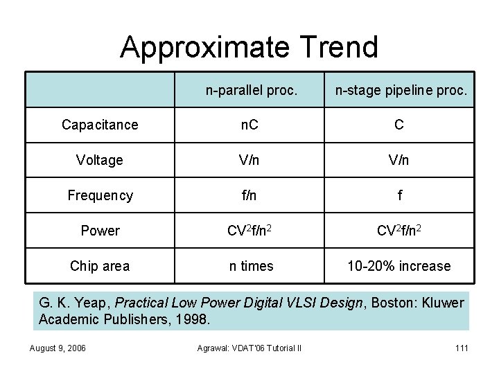
Approximate Trend n-parallel proc. n-stage pipeline proc. Capacitance n. C C Voltage V/n Frequency f/n f Power CV 2 f/n 2 Chip area n times 10 -20% increase G. K. Yeap, Practical Low Power Digital VLSI Design, Boston: Kluwer Academic Publishers, 1998. August 9, 2006 Agrawal: VDAT'06 Tutorial II 111

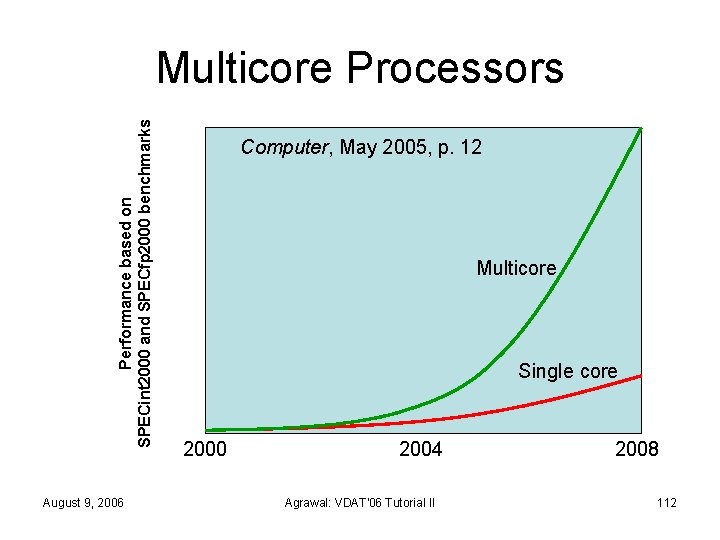
Performance based on SPECint 2000 and SPECfp 2000 benchmarks Multicore Processors August 9, 2006 Computer, May 2005, p. 12 Multicore Single core 2000 2004 Agrawal: VDAT'06 Tutorial II 2008 112

Multicore Processors • D. Geer, “Chip Makers Turn to Multicore Processors, ” Computer, vol. 38, no. 5, pp. 11 -13, May 2005. • A. Jerraya, H. Tenhunen and W. Wolf, “Multiprocessor Systems-on-Chips, ” Computer, vol. 5, no. 7, pp. 36 -40, July 2005; this special issue contains three more articles on multicore processors. • S. K. Moore, “Winner Multimedia Monster – Cell’s Nine Processors Make It a Supercomputer on a Chip, ” IEEE Spectrum, vol. 43. no. 1, pp. 20 -23, January 2006. August 9, 2006 Agrawal: VDAT'06 Tutorial II 113

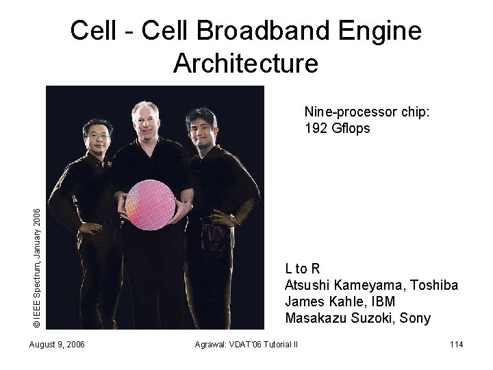
Cell - Cell Broadband Engine Architecture © IEEE Spectrum, January 2006 Nine-processor chip: 192 Gflops August 9, 2006 L to R Atsushi Kameyama, Toshiba James Kahle, IBM Masakazu Suzoki, Sony Agrawal: VDAT'06 Tutorial II 114

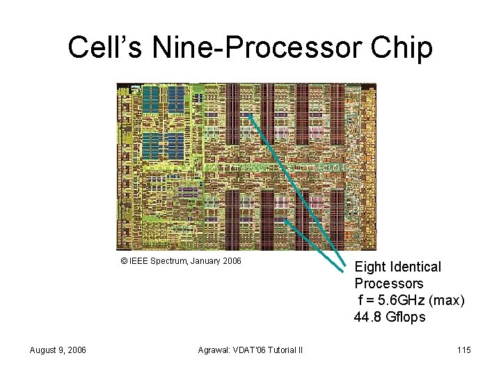
Cell’s Nine-Processor Chip © IEEE Spectrum, January 2006 August 9, 2006 Agrawal: VDAT'06 Tutorial II Eight Identical Processors f = 5. 6 GHz (max) 44. 8 Gflops 115

Books on Low-Power Design (1) • • • L. Benini and G. De Micheli, Dynamic Power Management Design Techniques and CAD Tools, Boston: Springer, 1998. T. D. Burd and R. A. Brodersen, Energy Efficient Microprocessor Design, Boston: Springer, 2002. A. Chandrakasan and R. Brodersen, Low-Power Digital CMOS Design, Boston: Springer, 1995. A. Chandrakasan and R. Brodersen, Low-Power CMOS Design, New York: IEEE Press, 1998. J. -M. Chang and M. Pedram, Power Optimization and Synthesis at Behavioral and System Levels using Formal Methods, Boston: Springer, 1999. M. S. Elrabaa, I. S. Abu-Khater and M. I. Elmasry, Advanced Low-Power Digital Circuit Techniques, Boston: Springer, 1997. R. Graybill and R. Melhem, Power Aware Computing, New York: Plenum Publishers, 2002. S. Iman and M. Pedram, Logic Synthesis for Low Power VLSI Designs, Boston: Springer, 1998. J. B. Kuo and J. -H. Lou, Low-Voltage CMOS VLSI Circuits, New York: Wiley. Interscience, 1999. J. Monteiro and S. Devadas, Computer-Aided Design Techniques for Low Power Sequential Logic Circuits, Boston: Springer, 1997. S. G. Narendra and A. Chandrakasan, Leakage in Nanometer CMOS Technologies, Boston: Springer, 2005. W. Nebel and J. Mermet, Low Power Design in Deep Submicron Electronics, Boston: Springer, 1997. August 9, 2006 Agrawal: VDAT'06 Tutorial II 116

Books on Low-Power Design (2) • • • • N. Nicolici and B. M. Al-Hashimi, Power-Constrained Testing of VLSI Circuits, Boston: Springer, 2003. V. G. Oklobdzija, V. M. Stojanovic, D. M. Markovic and N. Nedovic, Digital System Clocking: High Performance and Low-Power Aspects, Wiley-IEEE, 2005. M. Pedram and J. M. Rabaey, Power Aware Design Methodologies, Boston: Springer, 2002. C. Piguet, Low-Power Electronics Design, Boca Raton: Florida: CRC Press, 2005. J. M. Rabaey and M. Pedram, Low Power Design Methodologies, Boston: Springer, 1996. S. Roudy, P. K. Wright and J. M. Rabaey, Energy Scavenging for Wireless Sensor Networks, Boston: Springer, 2003. K. Roy and S. C. Prasad, Low-Power CMOS VLSI Circuit Design, New York: Wiley. Interscience, 2000. E. Sánchez-Sinencio and A. G. Andreaou, Low-Voltage/Low-Power Integrated Circuits and Systems – Low-Voltage Mixed-Signal Circuits, New York: IEEE Press, 1999. W. A. Serdijn, Low-Voltage Low-Power Analog Integrated Circuits, Boston: Springer, 1995. S. Sheng and R. W. Brodersen, Low-Power Wireless Communications: A Wideband CDMA System Design, Boston: Springer, 1998. G. Verghese and J. M. Rabaey, Low-Energy FPGAs, Boston: springer, 2001. G. K. Yeap, Practical Low Power Digital VLSI Design, Boston: Springer, 1998. K. -S. Yeo and K. Roy, Low-Voltage Low-Power Subsystems, Mc. Graw Hill, 2004. August 9, 2006 Agrawal: VDAT'06 Tutorial II 117

Other Books Useful in Low-Power Design • A. Chandrakasan, W. J. Bowhill and F. Fox, Design of High. Performance Microprocessor Circuits, New York: IEEE Press, 2001. • N. H. E. Weste and D. Harris, CMOS VLSI Design, Third Edition, Reading, Massachusetts, Addison-Wesley, 2005. • S. M. Kang and Y. Leblebici, CMOS Digital Integrated Circuits, New York: Mc. Graw-Hill, 1996. • E. Larsson, Introduction to Advanced System-on-Chip Test Design and Optimization, Springer, 2005. • J. M. Rabaey, A. Chandrakasan and B. Nikolić, Digital Integrated Circuits, Second Edition, Upper Saddle River, New Jersey: Prentice-Hall, 2003. • J. Segura and C. F. Hawkins, CMOS Electronics, How It Works, How It Fails, New York: IEEE Press, 2004. August 9, 2006 Agrawal: VDAT'06 Tutorial II 118