Lecture 19 Sensors of Structure Matter Waves and


 Where E=Young’s modulus (N/m")


Ψ=iħ dΨ/dt • All ‘waveicles’")
=0 between x=0")
=Asin(n*pi*x/L) inside the well – These are simply")
=Ae±ax outside the well – This is the important bit for")


 • E=Youngs modulus (N/m")


Ψ=iħ dΨ/dt • All ‘waveicles’")
=0 between x=0")
=Asin(n*pi*x/L) inside the well – These are simply")
=Ae±ax outside the well – This is the important bit for")

 exp(-2 L)")


")
 • STM measures tunelling current;")


 Combined with AFM • Optical resolution determined by")


")


 magnet induces strong diamagnetic field in the water.")


 /volume Where n is the")
 – M")


 • Ferromagnetism – Atoms have associated dipole moments – If")
 • For a Paramagnetic material M=CT(B/T) where C is the")
 • 1911:")


 • Used to detect presence of H atoms")


 insulating layer")


 • 1911: Resistance of")


 • Used to detect presence of")
 –")


 insulating layer")


- Slides: 144
Lecture 19
Sensors of Structure • • • Matter Waves and the de. Broglie wavelength Heisenberg uncertainty principle Electron diffraction Transmission electron microscopy Atomic-resolution sensors
Count Loius de Broglie • Postulated that all objects have a wavelength given by λ=h/p • λ=wavelength • h=Planck’s constant • p=momentum of object • In practice, only really small objects have a sensible wavelength
Wave-Particle duality • A consequence of the de. Broglie hypothesis is that all objects can be thought of as “wavicles”: both particles and waves • This has troubled many philosophically-minded scientists over the years. • Inescapable if we want to build atomic-resolution sensors.
Heisenberg’s “Uncertantity Principle” • Cannot simultaneously measure an object’s momentum and position to a better accuracy than ħ/2 Δpx Δx≥ħ/2 • Direct consequence of waveparticle duality • Places limitations on sensor accuracy
Electron Diffraction • Accelerated electrons have wavelength of order 1 Angstrom=1 x 10 -10 m • Same order as atomic spacing • Electrons undergo Bragg diffraction at atomic surfaces if the atoms are lined up in planes, (i. e. in a crystal)
Bragg reflection • Constructive interference when the path length difference is a integer multiple of the wavelengths • nλ=2 d sinθ • Detailed description requires heavy (mathematical) Quantum Mechanics.
Diffraction Patterns • Only certain angles of reflection are allowed. • The diffracted electrons form patterns. • In polycrystalline material, these are rings X-rays on left, electrons on right.
Davisson-Germer experiment • Application of diffraction to measure atomic spacing • Single crystal Ni target • Proved de. Broglie hypothesis that λ=h/p
Proof that λ=h/p Accelerated electrons have energy e. V: e. V= ½ mv 2 => v = (2 Ve/m)1/2 de Broglie said: λ=h/p=h/(mv)=h/(2 m. Ve)1/2=1. 67 Å Davisson-Germer found lattice spacing: λ=dsinθ=1. 65 Å Excellent agreement between theory and experiment!
Application: Pressure sensing • Atomic spacing changes with pressure: Pressure=E(ΔL/L) Where E=Young’s modulus (N/m 2) • As d (spacing between atomic planes) changes, the angle of diffraction changes • Diffraction rings move apart or closer together
STM and AFM • Electron diffraction can probe atomic lengthscales, but – Targets need to be crystalline – Need accelerated electrons=>bulky and expensive apparatus. – Need alternatives!
http: //www. personal. psu. edu/users/m/m/mmt 163/E%20 SC%20497 E_files/Quantum_Corral. htm Atomic level imaging and manipulation • Scanning Tunnelling Microscopy • Atomic Force Microscopy
Quantum Corral • Image shows ‘Quantum corral’ of 48 Fe atoms on a Cu surface • Low-temp STM used for assembly and imaging • Can see Schrodinger standing waves • Colors artificial
Quantum Mechanics • STM and AFM inherently quantummechanical in operation • Need to understand the electron wavefunction to understand their operation • We need some QM first
The wavefunction • The electrons of an atom are described by their wavefunction: – Ψ= Ψ 0 ei/ħ (px-Et) – Contains all information about electron • Eg probability of electron being in a certain region is P(x)=∫ Ψ*Ψdx
Schrodinger’s Eqn • -ħ/2 m d 2Ψ/dx 2 + U(x)Ψ=iħ dΨ/dt • All ‘waveicles’ must obey this eqn • U(x) is the potential well – In the case of atoms, it can be approximated by a square well
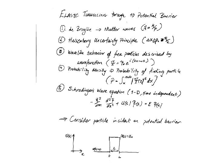
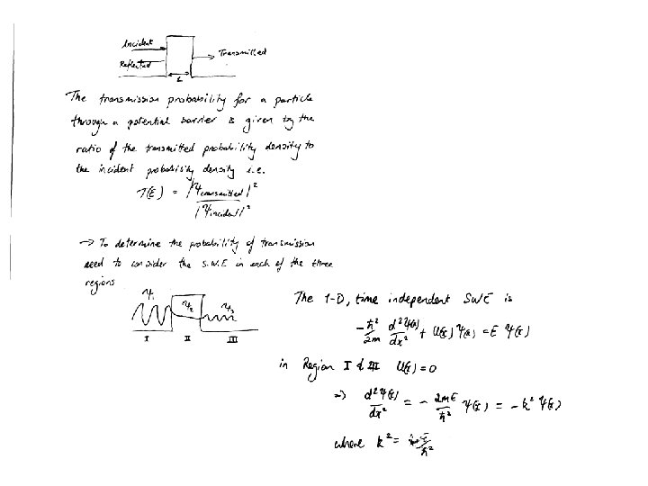
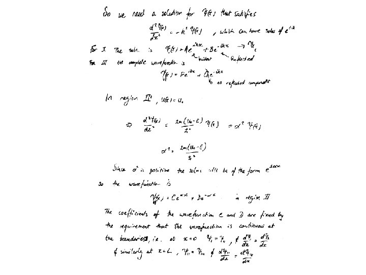
The square well • Solve Schrodinger’s eqn for a potential – U(x)=0 between x=0 and x=L – U(x)=U 0 everywhere else. • Assume that the solutions do not vary with time (stationary states) – Ψ= Ψ(x)
Solutions for a square well • Ψ(x)=Asin(n*pi*x/L) inside the well – These are simply standing waves in a cavity, with n denoting the mode number • Same as solution from classical physics
Wavefunction trails • Ψ(x)=Ae±ax outside the well – This is the important bit for STM and AFM – Means that the wavefunction extends beyond the atomic surface
Tunnelling phenomena • If another atom is brought close enough to the first, the wavefunction from the first atom can overlap into the second • Means electron has probablilty of being found in second atom • Electron has tunnelled through the potential barrier
In STM, a tip is brought in very close proximity to a surface to be analysed: the electrons can tunnel from tip to surface (or vice versa).
STM operation Tunnelling current very sensitive function of separation Keep tip current constant, and measure variations in height with a piezoelectric crystal
Lecture 20
Sensors of Structure • • • Matter Waves and the de. Broglie wavelength Heisenberg uncertainty principle Electron diffraction Transmission electron microscopy Atomic-resolution sensors
de. Broglie • Postulated that all objects have a wavelength given by – λ=h/p • λ=wavelength • h=Planck’s constant • p=momentum of object • In practice, only really small objects have a sensible wavelength
Wave-Particle duality • A consequence of the de. Broglie hypothesis is that all objects can be thought of as “wavicles”: both particles and waves • This has troubled many philosophicallyminded scientists over the years. • Inescapable if we want to build atomicresolution sensors.
Heisenberg Uncertantity Principle • Cannot simultaneously measure an object’s momentum and position to a better accuracy than ħ/2 – Δpx Δx≥ħ/2 • Direct consequence of wave-particle duality • Places limitations on sensor accuracy
Electron Diffraction • Accelerated electrons have wavelength of order 1 Angstrom=1 e-10 m • Same order as atomic spacing • Electrons undergo Bragg diffraction at atomic surfaces if the atoms are lined up in planes, ie a crystal
Bragg reflection • Constructive interference when the path length difference is a integer multiple of the wavelengths • nλ=2 d sinθ • Detailed description requires heavy (mathematical) QM.
Diffraction Patterns • Only certain angles of reflection are allowed. • The diffracted electrons form patterns. • In polycrystalline material, these are rings X-rays on left, electrons on right.
Davisson-Germer experiment • Application of diffraction to measure atomic spacing • Single crystal Ni target • Proved de. Broglie hypothesis that λ=h/p
Proof that λ=h/p Accelerated electrons have energy e. V: e. V= ½ mv 2 => v = (2 Ve/m)1/2 de Broglie said: λ=h/p=h/(mv)=h/(2 m. Ve)1/2=1. 67 Å Davisson-Germer found lattice spacing: λ=dsinθ=1. 65 Å Excellent agreement between theory and experiment!
Pressure sensing • Atomic spacing changes with pressure: – Pressure=E(ΔL/L) • E=Youngs modulus (N/m 2) • As d changes, angle of diffraction changes • Rings move apart or closer together
STM and AFM • Electron diffraction can probe atomic lengthscales, but – Targets need to be crystalline – Need accelerated electrons=>bulky and expensive apparatus. – Need alternatives!
http: //www. personal. psu. edu/users/m/m/mmt 163/E%20 SC%20497 E_files/Quantum_Corral. htm Atomic level imaging and manipulation • Scanning Tunnelling Microscopy • Atomic Force Microscopy
Quantum Corral • Image shows ‘Quantum corral’ of 48 Fe atoms on a Cu surface • Low-temp STM used for assembly and imaging • Can see Schrodinger standing waves • Colors artificial
Quantum Mechanics • STM and AFM inherently quantummechanical in operation • Need to understand the electron wavefunction to understand their operation • We need some QM first
The wavefunction • The electrons of an atom are described by their wavefunction: – Ψ= Ψ 0 ei/ħ (px-Et) – Contains all information about electron • Eg probability of electron being in a certain region is P(x)=∫ Ψ*Ψdx
Schrodinger’s Eqn • -ħ/2 m d 2Ψ/dx 2 + U(x)Ψ=iħ dΨ/dt • All ‘waveicles’ must obey this eqn • U(x) is the potential well – In the case of atoms, it can be approximated by a square well
The square well • Solve Schrodinger’s eqn for a potential – U(x)=0 between x=0 and x=L – U(x)=U 0 everywhere else. • Assume that the solutions do not vary with time (stationary states) – Ψ= Ψ(x)
Solutions for a square well • Ψ(x)=Asin(n*pi*x/L) inside the well – These are simply standing waves in a cavity, with n denoting the mode number • Same as solution from classical physics
Wavefunction trails • Ψ(x)=Ae±ax outside the well – This is the important bit for STM and AFM – Means that the wavefunction extends beyond the atomic surface
Atomic level imaging and manipulation • Scanning Tunnelling Microscopy • Atomic Force Microscopy
T(E) exp(-2 L)
Tunnelling phenomena • If another atom is brought close enough to the first, the wavefunction from the first atom can overlap into the second • Means the electron has probability of being found in second atom • Electron has tunnelled through the potential barrier
Transmitted intensity proportional to e-2 s Incident Where Transmitted Reflected Characteristic scale of tunnelling is δ=1/ If U-E =4 e. V (typical value of metal work function), then for an electron: δ=(1. 05*10 -34)/[(2(9. 1*10 -31)(4*1. 6*10 -19))]1/2 which is about 1 Å
STM Principles • “Scanning Tunnelling Microscope” • Tunnelling current depends exponentially on distance from surface – Move tip across surface, and the current changes as the tip “feels” the “bumps” caused by valence electron wave functions • Image shows individual atoms of a sample of Highly Oriented Pyrolytic Graphite.
In STM, a tip is brought in very close proximity to a surface to be analysed: the electrons can tunnel from tip to surface (or vice versa).
STM operation Tunnelling current very sensitive function of separation Keep tip current constant, and measure variations in height with a piezoelectric crystal
STM and piezos • Piezoelectric bar • Application of bias causes expansion contraction of crystal • Tube scanner – 2 -D scanning 0 V +V -V
STM Operating Modes • Const. current mode: – Move tip over surface and measure changes in height with piezo. • Const. height mode: – Keep tip-surface separation const, and measure changes in current. – Need very flat samples to avoid tip crash!
Raster Scanning over area from. 1 X. 1 mm to 10 X 10 nm Scan rates can be quite fast Resolution/scan size/scan rate tradeoff Scanning issues
Vacuum Operation • Needs Ultra-High vacuum – Prevents unwanted gases adsorbing onto surface – Lots of turbo pumps and stainless steel – Bakeout and surgical handling procedures
Atomic manipulation using STM • Can move or desorb atoms as well as image. • Adsorb=stick to surface • Desorb=unstick from surface • Absorb=diffuse into bulk • Put high voltage on tip to draw current and “arc weld surface” • Use small bias to pick up atoms and assemble them into cheesy logo
Some gratuitous STM images • Great for grant applications and press releases!
Nanoscale Lithography • Selective oxidation of semiconductor surfaces • Positioning of single atoms
The STM image • The STM image is a file of (x, y, height) co-ords • It can be manipulated to produce all sorts of images – Fantastic colour schemes of dubious taste – Animation and fly-by videos • Quantum corrals; can image e- wavefunction – See the ripples – Spiles are Fe d-orbitals – Yellow atoms are Cu
The Atomic Force Microscope • Atomic Force Microscope (AFM) • STM measures tunelling current; but AFM measures van der waals forces directly • Van der Vaals force attractive with FVDW 1/s 7
The AFM • Detect minute movements in cantilever by bouncing laser off and using interferometry (remember laser sensors) • Photodetector measures the difference in light intensities between the upper and lower photodetectors, and then converts to voltage. • Feedback from photodiode signals, enables the tip to maintain either a constant force or constant height above the sample. • Atomic resolution • Sample need not be electrically conductive
The AFM cantilever • Most critical component. • Low spring constant for detection of small forces (Hookes law F=-kx) • High resonant frequency to minimise sensitivity to mechanical vibrations (ωo 2=k/mc) • Small radius of curvature for good spatial resolution • High aspect ratio (for deep structures), can use nanotubes
AFM • Can get atomic scale resolution, just like STM. • Still needs UHV and vibration isolation for atomic scale resolution. • Different Modes: – Contact – Non-contact (resonant response of cantilever monitored)
Contact mode • Responds to short range interatomic forces – Variable deflection imaging • scan with no feedback, measure force changes across surface – Constant Force imaging • Force and cantilever deflection kept constant to image surface topography • Caution is required to ensure cantilever doesn’t damage surface
Non-Contact mode • Responds to long range interatomic forces greater sensitivity required • Instead of monitoring quasistatic cantilever deflections measure changes in resonant response of cantilever • Cantilever connected to piezoelectric element – bends with applied potential • Lower probability of inducing damage to surface piezo ac cantilever
• Cantilever driven close to resonant frequency, ωo • If cantilever has spring const, ko in absence of surface interactions • Then in presence of force gradient, F’=d. Fz/Dz Keff=ko-F’ • This causes shift in resonant frequency i. e ωeff 2=keff/mc=(ko-F’) /mc=(ko /mc)(1 - F’/ko) ωeff=ωo (1 - F’/ko)1/2 • If F’ small ωeff ~ωo (1 - F’/2 ko), hence a force gradient F will shift the resonant frequency
Near field Scanning Optical Microscope (NSOM) Combined with AFM • Optical resolution determined by diffraction limit (~λ) • Illuminating a sample with the "near-field" of a small light source. • Can construct optical images with resolution well beyond usual "diffraction limit", (typically ~50 nm. ) NSOM/AFM Probe SEM - 70 nm aperture
NSOM Setup Transmission Ideal for thin films or coatings which are several hundred nm thick on transparent substrates (e. g. , a round, glass cover slip). Photoluminescence emsission Sample locally illuminated with SNOM, spectrally resolved global photemission measured.
Lecture 21
The STM Tip – Tunnelling current very sensitive function of separation – Keep tip current constant, and measure variations in height with a piezoelectric crystal. Tip Atoms Tunnelling electrons Surface Atoms
STM Principles • “Scanning Tunnelling Microscope” • Tunnelling current depends exponentially on distance from surface – Move tip across surface, and the current changes as the tip “feels” the “bumps” caused by valence electron wave functions • Image shows individual atoms of a sample of Highly Oriented Pyrolytic Graphite.
STM Operating Modes • Const. current mode: – Move tip over surface and measure changes in height with piezo. • Const. height mode: – Keep tip-surface separation const, and measure changes in current. – Need very flat samples to avoid tip crash!
Scanning Raster Scanning over area from. 1 X. 1 mm to 10 X 10 nm Scan rates can be quite fast Resolution/scan size/scan rate tradeoff
Vacuum Sucks • Needs Ultra-High vacuum – Otherwise unwanted gases adsorb onto surface – Lots of turbo pumps and stainless steel – Bakeout and surgical handling procedures
The STM • Can move or desorb atoms as well as image. • Adsorb=stick to surface • Desorb=unstick from surface • Absorb=diffuse into bulk – Put high voltage on tip to draw current and “arc weld surface” – Use small bias to pick up atoms and assemble them into cheesy logo
The STM image • The STM image is a file of (x, y, height) co-ords • It can be manipulated to produce all sorts of images – Fantastic colour schemes of dubious taste – Animation and fly-by videos • Quantum corrals; can image e - wavefunction – See the ripples – Spiles are Fe d-orbitals – Red atoms are Cu
Gratuitous STM images • Great for grant applications and press releases
The AFM • Atomic Force Microscope • STM measures tunelling current; but AFM measures van der waals forces directly
The AFM • Detect minute movements in cantilever by bouncing laser off and using interferometry (remember laser sensors) • Atomic resolution • Sample need not be electrically conductive
AFM • Can get atomic scale resolution, just like STM. • Still needs UHV and vibration isolation for atomic scale resolution. • Different Modes: – Contact – Non-contact – Tapping
Lecture 22
Lecture 23
Remember Dielectric Materials? • Many molecules and crystals have a non-zero Electric dipole moment. • When placed in an external electric field these align with external field. • The effect is to reduce the strength of the electric field within the material. • To incorporate this, we define a new vector Field, the electric displacement,
Diamagnetism • Polarisation of dielectrics involves the creation of induced electric dipoles by an external electric field • The equivalent effect for magnetic materials is diamagnetism • The atoms in a diamagnet alter their electron orbits in order to oppose the field • Diamagnet acts like a bar magnet and repels external field • Water is a diamagnet-hence the levitating frog!
Levitating Frog • Huge (20 T) magnet induces strong diamagnetic field in the water. • Force is strong enough to levitate frog
Paramagnetism • In some materials, there are permanent magnetic moments. • When an external magnetic field is applied, these line up with the field to reinforce it • This is a much stronger effect than diamagnetism, and in the opposite effect • Ferromagnetism is a form of paramagnetism • Where do these permanent magnetic moments originate from?
Magnetisation Some atoms have unpaired electrons. Each unpaired electron possess a magnetic dipole moment, μ, which is an integer multiple of μB=eħ/2 me (The Bohr Magneton) In essence, consider the atoms as tiny magnets. The magnetic moments arise from both the spin and orbital motion of the electrons. ) e
Magnetisation Thus some materials have a magnetisation M= (nμ) /volume Where n is the number of dipoles present M may also depend on external factors like temperature or magnetic field So some matter produces its own magnetic field Bm= μ 0 M (Where μ 0 is the permeability of vacuum)
More magnetisation • B=B 0+Bm • Introduce magnetic field strength H=(B /μo) – M • Thus B= μo(H+M) • Total field=External field + Field due to material • Consider current through coils with n loops/metre • Empty coil: B= μ 0 H so H=n. I • Coil with material inside (ie a core) H=n. I still, but enhanced B if contribution (M) from material in core
Dia-, Para-, Ferro-, … • Magnetisation M depends on magnetic field strength H via M=χH χ =magnetic susceptibility • χ >0 =>paramagnetic (boosts applied field) • χ <0 =>diamagnetic (reduces applied field) Ferromagnetism can be thought of as an extreme case of paramagnetism with a variable χ (typically χ>>0 for Ferromagnetic material).
Remember these Ferromagnetism demos?
Atomic level view (I) • Ferromagnetism – Atoms have associated dipole moments – If dipoles aligned net B-field. – At higher Temperatures thermal agitation reduces alignment – Presence of external field alignment of dipoles, Removal of field alignment remains – Thus explain hysterisis • Paramagnetism – Atoms have associated dipole moments but only interact weakly with each other – In the absence of external field no net magnetisation – In presence of external field some alignment but must compete with thermal agitation
Atomic level view (II) • For a Paramagnetic material M=CT(B/T) where C is the Curie constant – Hence for paramagnetic material M increases at low T • Diamagnetism – Atoms have no associated dipole moments (even number of outer shell electrons) – Presence of external field weak dipole moment which opposes applied field (Lenz’s Law). – Removal of field alignment disappears
Superconductivity: A Historical introduction • 1908: He first liquefied ( by Onnes) • 1911: Observed that resistance of liquid Hg plummets at 4. 2 K • This ultra-low resistance termed superconductivity
• 1933: Meissner – Magnetic field is expelled from superconductor – Superconductivity ceases at B >Bc – More about this later • 1962: Josephson Junction – Two superconductors separated by a thin insulating oxide barrier • 1986: High Tc (150 K) Superconductors
Types of superconductors • There are two main classes of superconductor: – Type I - (e. g. Hg) have a critical field and a critical temperature above which they abruptly cease superconducting – Type II - have an intermediate phase, which extends to higher temperatures and fields.
Type I superconductors • Mostly single element metals • Superconductivity destroyed for T>Tc or B>Bc • Variation of Bc with temperature can be expressed as • Low value of Bc (typically < 0. 1 T) means generating strong magnetic fields using type I superconductors not possible
Examples of type I superconductors
Meissner Effect • Inside the superconductor – J=σE for all conductors, but superconductors have σ infinite, so electric field is zero even when a current flows – Faraday’s Law says ∫E. d. S=-dφ/dt where φ=magnetic flux • E=0 => φ=const • B= φ/Area so B becomes “trapped” inside.
Meissner effect • If we put a perfect conductor in an external magnetic field at T>Tc, then cool to T<Tc, then remove field, we expect some field trapped inside. • In fact, B=0 always inside a superconductor at T<Tc, B<Bc. • Superconductor is a perfect diamagnet, and hence repels permanent magnets.
Type II superconductors • Mostly alloys and whizzy ceramics • At fields between Bc 1 and Bc 2 some flux lines penetrate • At B> Bc 2 these flux lines overlap and superconductivity dies • Bc 2 very large (<30 T), so these materials suitable for superconducting magnets
Some type II superconductors
Worked example • A solenoid is to be constructed using Nb 3 Al (Bc 2=32 T). The wire has a radius of 1. 0 mm, and the solenoid is to be wound on a cylinder of diameter 8. 00 cm and length 90. 0 cm. There are 150 turns per cm of length. How much current is required to get a field of 5. 0 T at the centre? • B=μ 0 n. I – N=150 turns/cm=1. 5 x 10⁴ turns/m; – B= 5. 0 T – I=B/nμ 0=265 Amps
Useful properties • Persistent currents B – Once a current has been set up in the loop, it keeps going ‘forever’ (R < 1 e 26 Ωm) • Flux trapping – Consider superconducting loop, T>Tc – Apply B field, then cool to T<Tc – Field is trapped inside the loop, but expelled from the material – Trapped flux is quantised in units of h/2 e, “magnetic flux quantum”, o=2. 0678 x 10 -15 T. m 2 T>Tc T<Tc
Applications of superconductivity (Magnetic Resonance Imaging) • Used to detect presence of H atoms • Magnetic resonance imager has 1. 5 Tesla superconducting magnet • Once current is caused to flow in the coil it will continue to flow as long as the coil is kept at liquid helium temperatures. • losses of the order of one part per million of the main magnetic field per year. http: //www. cis. rit. edu/htbooks/mri/ Copyright © 1996 -2003 J. P. Hornak.
Mechanism of Superconductivity • How can an electron possibly travel through a material without being scattered? • Clue: Isotope effect showed dependence on atomic number of lattice atoms • Normal conductivity independent of lattice (unless defects are present)
Cooper Pairs
Cooper Pairs • e- with opposite momentums and spins form single particle • Cooper pairs are bosons, e- are fermions • Pairs no longer have to obey Pauli exclusion principle • All Cooper pairs are in the same state! • Individual e- not free to scatter off lattice impurities
More about Cooper pairs • They are all in phase and locked in with each other over the entire sample volume • All the Cooper pairs form a coherent state • If we provide enough energy, we can break up the pair, destroying superconductivity • This energy is Eg=3. 53 k. BTc • Leads to a “band gap”, analagous to semiconductors
Josephson Junctions • 2 pieces of superconductor, separated by thin (~10 Å) insulating layer • Tunnelling of bound pair through insulating layer possible Superconducting material Insulating Layer (oxide) • Unique effects associated with pair tunnelling Ψ 1 Ψ 2 sc 1 oxide
The DC Josephson effect • At zero voltage there exists a superconducting current given by Is=Imaxsin(φ1 -φ2)=Imaxsin(δ) Dependant on thickness of insulating layer and junction area Phase difference between the wavefunctions in the two superconductors • Imax is the maximum current across the junction under zero bias conditions
The AC Josephson effect • A DC voltage across a Josephson junction generates an alternating current given by Is=Imaxsin(δ+2πft) where f=2 e. V/h • Hence Josephson current oscillates at frequency proportional to applied voltage • Is used as method of determining voltage standard – microwave current passed through junction – Stable operation only possible for voltages satisfying V=nhf/2 e (n is interger)
SQUIDs • “Superconducting QUantum Interference Devices” • Consist of 2 or more Josephson junctions in parallel • Extremely sensitive to changes in magnetic field Superconductor Junctions I
SQUIDs • Interference caused by difference in phase of the arrival of the current through two different paths • Analogous to optical interference (Young’s slits) • Difference in phase Δδ given by Δδ=δa -δb=(2 q/ħ) where is the flux passing through the loop • Hence the phase difference is dependant on the flux passing through the loop Ib Ia Junctions I
SQUIDs • The maximum current through the loop can be shown to be Imax=Iocos(q /ħ) • Hence current maxima observed for = nπħ/q • The Interference between two junctions can be used to make very sensitive measurement of magnetic field I B
Applications of SQUIDs • Biomagnetism – Some processes in animals/humans produce very small magnetic fields. The only type of detector sensitive enough to measure such a field is a SQUID. – Magnetoencephalography (MEG) the imaging of the human brain. Involves measuring the magnetic field produced by the currents due to neural activity. – Advantages other methods which only image the structure of the brain • Non Destructive testing – Potential uses in monitoring internal faults or wear in metal containing structures.
Lecture 24
History of Superconductivity • 1908: Liquid He first discovered (Onnes) • 1911: Resistance of liquid Hg plummets at 4. 2 K • Superconductors have zero resistance!
History of Superconductivity • 1933: Meissner – Magnetic field is expelled from superconductor – Superconductivity ceases at B >Bc • 1962: Josephson Junction – Two superconductors separated by a thin insulating oxide barrier • 1986: High Tc (150 K) Superconductors
Types of superconductors • There are two main types of superconductor: – Type I - (eg Hg) have a critical field and a critical temperature above which they stop superconducting – Type II - have an intermediate phase, which extends to higher temperatures and fields.
Type I superconductors • Mostly single element metals • Superconductivity destroyed for T>Tc or B>Bc • Variation of Bc with temperature can be expressed as • The low value of Bc (typicall <0. 1 T) generating strong magnetic fields using type I superconductors not possible
Type I superconductors
Meissner Effect • Inside the superconductor – J=σE for all conductors, but superconductors have σ infinite, so electric field is zero even when a current flows – Faraday’s Law says ∫E. d. S=-dφ/dt • φ=magnetic flux • E=0 => φ=const • B= φ/Area so B becomes “trapped” inside.
Meissner effect • If we put a perfect conductor in a field at T>Tc, then cool to T<Tc, then remove field, expect field trapped inside. • In fact, B=0 always inside a superconductor at T<Tc, B<Bc. • Superconductor is a perfect diamagnet, and hence repels permanent magnets.
Type II superconductors • Mostly alloys and whizzy ceramics • At fields between Bc 1 and Bc 2 some flux lines penetrate • At B> Bc 2 these flux lines overlap and superconductivity dies • Bc 2 very large (<30 T), so these materials suitable for superconducting magnets
Type II superconductors
Worked example • A solenoid is to be constructed using Nb 3 Al (Bc 2=32 T). The wire has a radius of 1. 0 mm, and the solenoid is to be wound on a cylinder of diameter 8. 00 cm and length 90. 0 cm. There are 150 turns per cm of length. How much current is required to get a field of 5. 0 T at the centre? • B=μ 0 n. I – N=150 turns/cm=1. 5 e 4 turns/m; – B= 5. 0 T – I=B/nμ 0=265 Amps
Useful properties • Persistent currents B – Once a current has been set up in the loop, it keeps going ‘forever’ (R < 1 e 26 Ωm) • Flux trapping – Consider superconducting loop, T>Tc – Apply B field, then cool to T<Tc – Field is trapped inside the loop, but expelled from the material – Trapped flux is quantised in units of h/2 e, “magnetic flux quantum”, o=2. 0678 x 10 -15 T. m 2 T>Tc T<Tc
Applications of superconductivity (Magnetic Resonance Imaging – MRI) • Used to detect presence of H atoms • Magnetic resonance imager has 1. 5 Tesla superconducting magnet • Once current is caused to flow in the coil it will continue to flow as long as the coil is kept at liquid helium temperatures. • losses of the order of a ppm of the main magnetic field per year. http: //www. cis. rit. edu/htbooks/mri/ Copyright © 1996 -2003 J. P. Hornak.
Devices based on superconductors • Josephson Junctions • Superconducting QUantum Interference Devices (SQUIDS) – Highly sensitive magnetic field detectors • To understand these, need to understand mechanisms responsible for superconductivity
Mechanism of Superconductivity • For normal conductor behaviour the resistivity is due to scattering from lattice ions or impurities • How can an e- possible travel through a material without being scattered? • Clue: Isotope effect showed dependence on atomic number lattice atoms • Normal conductivity independent of lattice (unless defects)
Mechanism of Superconductivity • The features of superconductiviy can be explained using theory developed by Bardeen, Cooper and Schrieffer (BCS theory) • Main Features of BCS Theory – 2 electrons in a superconductor can form a bound pair via an attractive interaction – known as a cooper pair • How can negatively charged electrons form bound pair? – Net attraction possible if electron interact via motion of crystal lattice
Cooper Pairs • Lattice momentarily deformed by passing electron (electron causes nearby lattice ions to move inwards) • This results in a slight increase in positive charge in this region • 2 nd electron sees the positive charge of the distorted region and is attracted towards it
Cooper Pairs • Paired electrons possess opposite momentums and spins form single particle • Cooper pairs are bosons, electrons are fermions • Pairs no longer have to obey Pauli exclusion principle • All Cooper pairs are in the same state! (all or nothing behaviour of superconductivity) • Individual electrons not free to scatter off lattice impurities
More Cooper pairs • All the cooper pairs form a coherent state • They are all in phase and locked in with each other over the entire sample volume • If we provide enough energy, we can break up the pair, destroying superconductivity • This energy is Eg=3. 53 k. BTc • Leads to a “band gap”, analagous to semiconductors
Josephson Junctions • 2 pieces of superconductor, separated by thin (~10 Å) insulating layer • Tunnelling of bound pair through insulating layer possible Superconducting material Insulating Layer (oxide) • Unique effects associated with pair tunnelling Ψ 1 Ψ 2 sc 1 oxide
The DC Josephson effect • At zero voltage there exists a superconducting current given by Is=Imaxsin(φ1 -φ2)=Imaxsin(δ) Dependant on thickness of insulating layer and junction area Phase difference between the wavefunctions in the two superconductors • Imax is the maximum current across the junction under zero bias conditions
The AC Josephson effect • A DC voltage across a Josephson junction generates an alternating current given by Is=Imaxsin(δ+2πft) where f=2 e. V/h • Hence Josephson current oscillates at frequency proportional to applied voltage • Is used as method of determining voltage standard – microwave current passed through junction – Stable operation only possible for voltages satisfying V=nhf/2 e (n is interger)
SQUIDs • “Superconducting QUantum Interference Devices” • Consist of 2 or more Josephson junctions in parallel • Extremely sensitive to changes in magnetic field Superconductor Junctions I
SQUIDs • Interference caused by difference in phase of the arrival of the current through two different paths • Analogous to optical interference (Young’s slits) • Difference in phase Δδ given by Δδ=δa -δb=(2 q/ħ) where is the flux passing through the loop • Hence the phase difference is dependant on the flux passing through the loop Ib Ia Junctions I
SQUIDs • The maximum current through the loop can be shown to be Imax=Iocos(q /ħ) • Hence current maxima observed for = nπħ/q • The Interference between two junctions can be used to make very sensitive measurement of magnetic field I B
Applications of SQUIDs • Biomagnetism – Some processes in animals/humans produce very small magnetic fields. The only type of detector sensitive enough to measure such a field is a SQUID. – Magnetoencephalography (MEG) the imaging of the human brain. Involves measuring the magnetic field produced by the currents due to neural activity. – Advantages other methods which only image the structure of the brain • Non Destructive testing – Potential uses in monitoring internal faults or wear in metal containing structures.