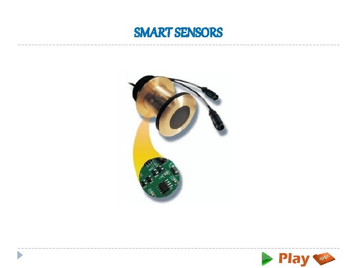
SMART SENSORS What is a smart sensor Smart


- Slides: 12

SMART SENSORS

What is a smart sensor? Ø Smart sensors are "sensors and instrument packages that are microprocessor driven and include features such as communication capability and onboard diagnostics that provide information to a monitoring system and/or operator to increase operational efficiency and reduce maintenance costs. "

General Architecture of Smart Sensor Ø Sensing element/transduction element, Ø Amplifier, Ø Sample and hold, Ø Analog multiplexer, Ø Analog to digital converter (ADC), Ø Offset and temperature compensation, Ø Digital to analog converter (DAC), Ø Memory, Ø Serial communication Ø Processor

Types of Smart Sensors Ø Optical Sensor Ø Infrared detector array Ø Accelerometer Ø Integrated multisensor

Optical Sensor Ø Optical sensor is one of the examples of smart sensor, which are used for measuring exposure in cameras, optical angle encoders and optical arrays. Similar examples are load cells silicon based pressure sensors.

Infrared detector array Integrated sensor is the infrared detector array developed at the solid laboratory of the University of Michigan. Ø The Infrared-sensing element was developed using polysilicon -Au thermocouples and thin film dielectric diaphragm to support thermocouples. Ø On-chip multiplexer was fabricated by using silicon gate MOS processing. Ø This detector operates over a temperature range of 0 to 100 degree centigrade with a 10 msec response time. Ø

Accelerometer Ø Accelerometer fabricated at the IBM Research laboratory at San Jose California, which consists of the sensing element and electronics on silicon. Ø The accelerometer itself is a metal-coated Si. O 2 cantilever beam that is fabricated on silicon chip where the capacitance between the beam and the substrate provides the output signal.

Integrated multisensor chip developed at the electronics research Laboratory University of California. Ø This chip contains MOS devices for signal conditioning with on chip sensor, a gas flow sensor, an infrared sensing array, a chemical reaction sensor, a cantilever beam, accelerometer, surface acoustic wave vapor sensor, a tactile sensor array and an infrared charge coupled device imager. Ø This chip was fabricated using conventional silicon planer processing, silicon micromachining and thin deposition techniques. Ø

Advantages Ø Minimum Interconnecting Cables Ø High Reliability Ø High Performance Ø Easy to Design, Use and Maintain Ø Scalable -Flexible System Ø Small Rugged Packaging Ø Minimum Cost

Applications Ø Bluetooth Smart Sensor Module Rear Panel. In-chamber and on-wafer sensors. Ø Monitoring of Temperature Using Smart Sensors Based on CAN Architecture. Ø Compatible sensors with microprocessors. Smart sensors vie for vision applications: smart sensors can provide the functionality needed for simple, low-cost machine-vision applications. Ø A Smart Sensor Architecture for Marine Sensor Networks

Conclusion Ø Smart Sensors has developed and proved a new miniaturized Smart Sensor Network Measurement System, which represents a paradigm shift from a centralized to a distributed processing measurement approach. Ø It significantly reduces the number and lengths of cables, the components size, and system weight. It provides greater flexibility in design, configuration and installation. Ø All of these advantages translate into cost savings throughout the life of a program.

Thank You www. playppt. com