EECS 150 Components and Design Techniques for Digital





![casex Example // Priority encoder module encode (A, valid, Y); input [7: 0] A; casex Example // Priority encoder module encode (A, valid, Y); input [7: 0] A;](https://slidetodoc.com/presentation_image_h/0da6a8610b4bf26dcd462e92d9514fd1/image-46.jpg)
- Slides: 49

EECS 150 - Components and Design Techniques for Digital Systems Lec 04 – Hardware Description Languages / Verilog 9/9 -04 David Culler Electrical Engineering and Computer Sciences University of California, Berkeley http: //www. eecs. berkeley. edu/~culler http: //www-inst. eecs. berkeley. edu/~cs 150 1

Review • Advancing technology changes the trade-offs and design techniques – 2 x transistors per chip every 18 months • ASIC, Programmable Logic, Microprocessor • Programmable logic invests chip real-estate to reduce design time & time to market • FPGA: – programmable interconnect, – configurable logic blocks » LUT + storage – Block RAM – IO Blocks 2

Outline • • • Netlists Design flow What is a HDL? Verilog Announcements Structural models Behavioral models Elements of the language Lots of examples 3

Remember: to design is to represent • How do we represent digital designs? • Components – Logic symbol, truth table – Storage symbol, timing diagram • Connections – Schematics Human readable or machine readable? ? ? 4

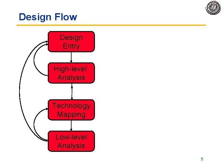
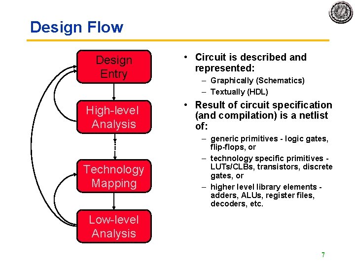
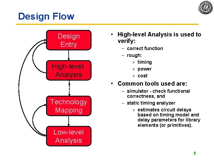
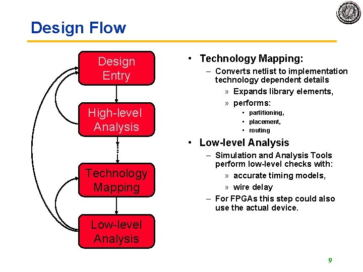
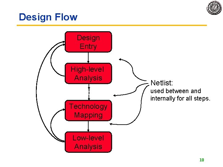
Design Flow Design Entry High-level Analysis Technology Mapping Low-level Analysis 5

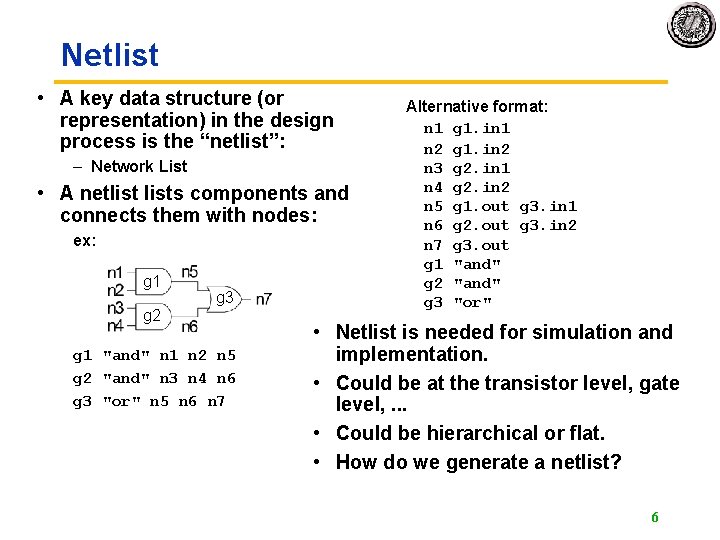
Netlist • A key data structure (or representation) in the design process is the “netlist”: – Network List • A netlists components and connects them with nodes: ex: g 1 g 3 g 2 g 1 "and" n 1 n 2 n 5 g 2 "and" n 3 n 4 n 6 g 3 "or" n 5 n 6 n 7 Alternative format: n 1 g 1. in 1 n 2 g 1. in 2 n 3 g 2. in 1 n 4 g 2. in 2 n 5 g 1. out g 3. in 1 n 6 g 2. out g 3. in 2 n 7 g 3. out g 1 "and" g 2 "and" g 3 "or" • Netlist is needed for simulation and implementation. • Could be at the transistor level, gate level, . . . • Could be hierarchical or flat. • How do we generate a netlist? 6

Design Flow Design Entry High-level Analysis Technology Mapping • Circuit is described and represented: – Graphically (Schematics) – Textually (HDL) • Result of circuit specification (and compilation) is a netlist of: – generic primitives - logic gates, flip-flops, or – technology specific primitives LUTs/CLBs, transistors, discrete gates, or – higher level library elements adders, ALUs, register files, decoders, etc. Low-level Analysis 7

Design Flow Design Entry High-level Analysis • High-level Analysis is used to verify: – correct function – rough: » timing » power » cost • Common tools used are: Technology Mapping – simulator - check functional correctness, and – static timing analyzer » estimates circuit delays based on timing model and delay parameters for library elements (or primitives). Low-level Analysis 8

Design Flow Design Entry High-level Analysis • Technology Mapping: – Converts netlist to implementation technology dependent details » Expands library elements, » performs: • partitioning, • placement, • routing • Low-level Analysis Technology Mapping – Simulation and Analysis Tools perform low-level checks with: » accurate timing models, » wire delay – For FPGAs this step could also use the actual device. Low-level Analysis 9

Design Flow Design Entry High-level Analysis Netlist: used between and internally for all steps. Technology Mapping Low-level Analysis 10

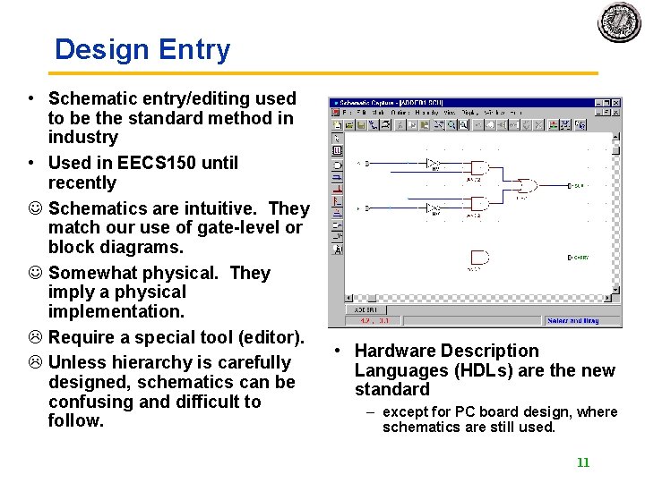
Design Entry • Schematic entry/editing used to be the standard method in industry • Used in EECS 150 until recently J Schematics are intuitive. They match our use of gate-level or block diagrams. J Somewhat physical. They imply a physical implementation. L Require a special tool (editor). L Unless hierarchy is carefully designed, schematics can be confusing and difficult to follow. • Hardware Description Languages (HDLs) are the new standard – except for PC board design, where schematics are still used. 11

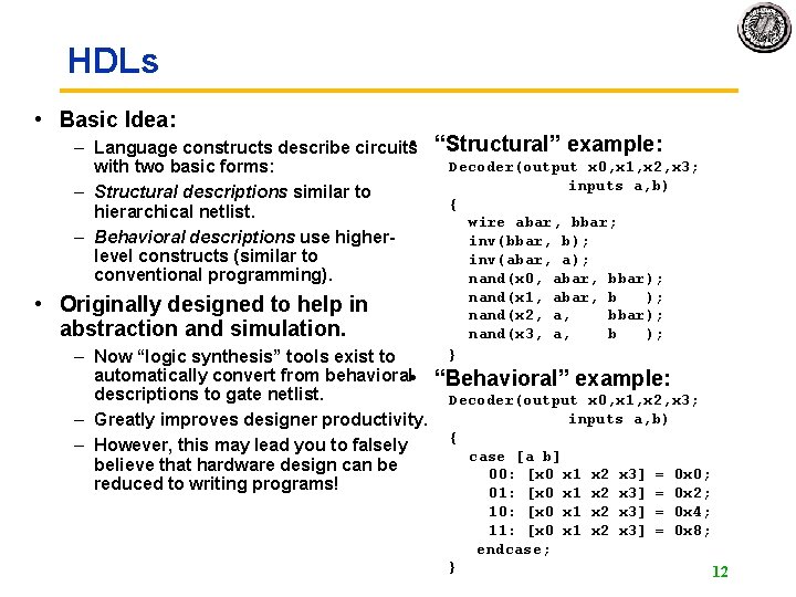
HDLs • Basic Idea: • – Language constructs describe circuits with two basic forms: – Structural descriptions similar to hierarchical netlist. – Behavioral descriptions use higherlevel constructs (similar to conventional programming). • Originally designed to help in abstraction and simulation. – Now “logic synthesis” tools exist to automatically convert from behavioral • descriptions to gate netlist. – Greatly improves designer productivity. – However, this may lead you to falsely believe that hardware design can be reduced to writing programs! “Structural” example: Decoder(output x 0, x 1, x 2, x 3; inputs a, b) { wire abar, bbar; inv(bbar, b); inv(abar, a); nand(x 0, abar, bbar); nand(x 1, abar, b ); nand(x 2, a, bbar); nand(x 3, a, b ); } “Behavioral” example: Decoder(output x 0, x 1, x 2, x 3; inputs a, b) { case [a b] 00: [x 0 x 1 x 2 x 3] = 0 x 0; 01: [x 0 x 1 x 2 x 3] = 0 x 2; 10: [x 0 x 1 x 2 x 3] = 0 x 4; 11: [x 0 x 1 x 2 x 3] = 0 x 8; endcase; } 12

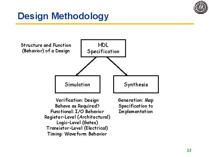
Design Methodology Structure and Function (Behavior) of a Design HDL Specification Simulation Synthesis Verification: Design Behave as Required? Functional: I/O Behavior Register-Level (Architectural) Logic-Level (Gates) Transistor-Level (Electrical) Timing: Waveform Behavior Generation: Map Specification to Implementation 13

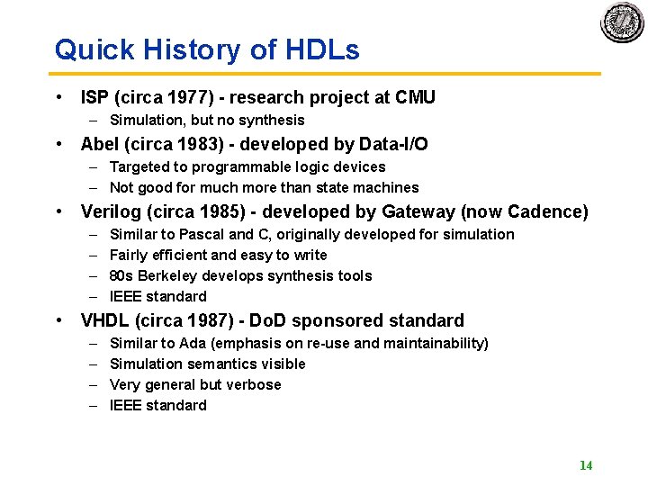
Quick History of HDLs • ISP (circa 1977) - research project at CMU – Simulation, but no synthesis • Abel (circa 1983) - developed by Data-I/O – Targeted to programmable logic devices – Not good for much more than state machines • Verilog (circa 1985) - developed by Gateway (now Cadence) – – Similar to Pascal and C, originally developed for simulation Fairly efficient and easy to write 80 s Berkeley develops synthesis tools IEEE standard • VHDL (circa 1987) - Do. D sponsored standard – – Similar to Ada (emphasis on re-use and maintainability) Simulation semantics visible Very general but verbose IEEE standard 14

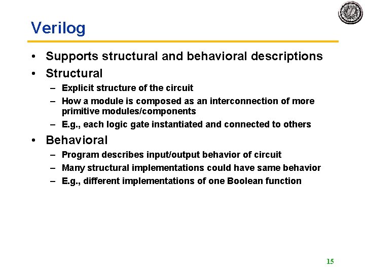
Verilog • Supports structural and behavioral descriptions • Structural – Explicit structure of the circuit – How a module is composed as an interconnection of more primitive modules/components – E. g. , each logic gate instantiated and connected to others • Behavioral – Program describes input/output behavior of circuit – Many structural implementations could have same behavior – E. g. , different implementations of one Boolean function 15

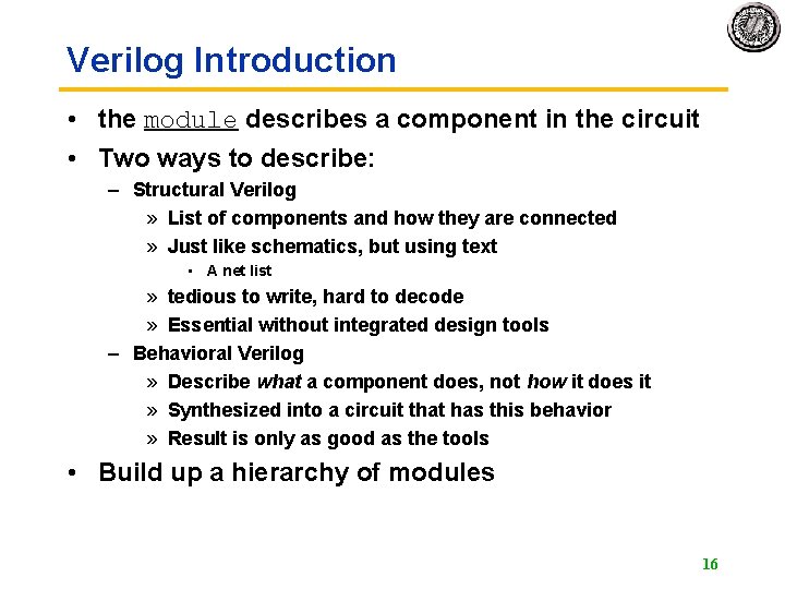
Verilog Introduction • the module describes a component in the circuit • Two ways to describe: – Structural Verilog » List of components and how they are connected » Just like schematics, but using text • A net list » tedious to write, hard to decode » Essential without integrated design tools – Behavioral Verilog » Describe what a component does, not how it does it » Synthesized into a circuit that has this behavior » Result is only as good as the tools • Build up a hierarchy of modules 16

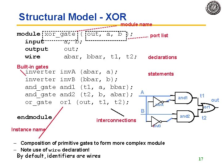
Structural Model - XOR module name module xor_gate ( out, a, b ); input a, b; output out; wire abar, bbar, t 1, t 2; Built-in gates inverter and_gate or_gate endmodule inv. A (abar, a); inv. B (bbar, b); and 1 (t 1, a, bbar); and 2 (t 2, b, abar); or 1 (out, t 1, t 2); port list declarations statements A and 1 t 1 inv. A or 1 B and 2 interconnections Instance name t 2 inv. B – Composition of primitive gates to form more complex module – Note use of wire declaration! By default, identifiers are wires 17 out

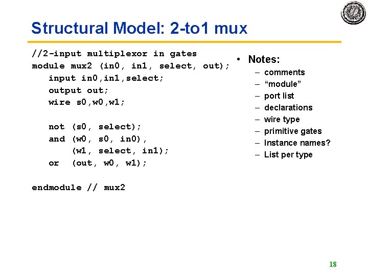
Structural Model: 2 -to 1 mux //2 -input multiplexor in gates • Notes: module mux 2 (in 0, in 1, select, out); – comments input in 0, in 1, select; – “module” output out; – port list wire s 0, w 1; not (s 0, select); and (w 0, s 0, in 0), (w 1, select, in 1); or (out, w 0, w 1); – – – declarations wire type primitive gates Instance names? List per type endmodule // mux 2 18

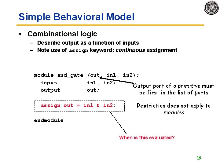
Simple Behavioral Model • Combinational logic – Describe output as a function of inputs – Note use of assign keyword: continuous assignment module and_gate (out, in 1, in 2); input in 1, in 2; Output port of a primitive must output out; be first in the list of ports assign out = in 1 & in 2; Restriction does not apply to modules endmodule When is this evaluated? 19

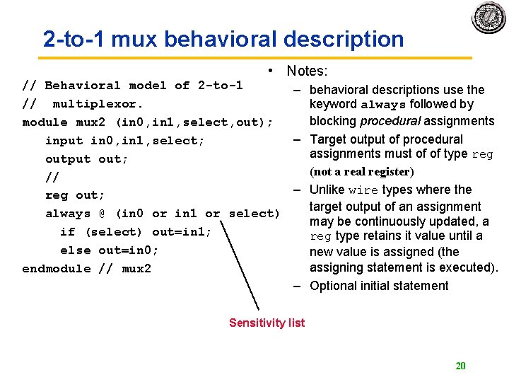
2 -to-1 mux behavioral description • Notes: // Behavioral model of 2 -to-1 – behavioral descriptions use the // multiplexor. keyword always followed by blocking procedural assignments module mux 2 (in 0, in 1, select, out); – Target output of procedural input in 0, in 1, select; assignments must of of type reg output out; (not a real register) // – Unlike wire types where the reg out; target output of an assignment always @ (in 0 or in 1 or select) may be continuously updated, a if (select) out=in 1; reg type retains it value until a else out=in 0; new value is assigned (the assigning statement is executed). endmodule // mux 2 – Optional initial statement Sensitivity list 20

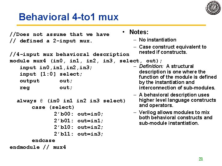
Behavioral 4 -to 1 mux //Does not assume that we have // defined a 2 -input mux. • Notes: – No instantiation – Case construct equivalent to nested if constructs. //4 -input mux behavioral description module mux 4 (in 0, in 1, in 2, in 3, select, out); – Definition: A structural input in 0, in 1, in 2, in 3; description is one where the input [1: 0] select; function of the module is defined output out; by the instantiation and reg out; interconnection of sub-modules. always @ (in 0 in 1 in 2 in 3 select) case (select) 2’b 00: out=in 0; 2’b 01: out=in 1; 2’b 10: out=in 2; 2’b 11: out=in 3; endcase endmodule // mux 4 – A behavioral description uses higher level language constructs and operators. – Verilog allows modules to mix both behavioral constructs and sub-module instantiation. 21

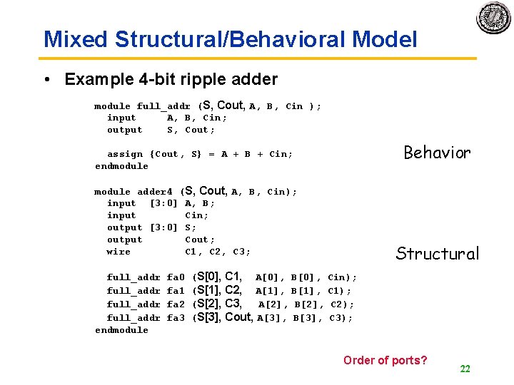
Mixed Structural/Behavioral Model • Example 4 -bit ripple adder module full_addr (S, Cout, A, B, Cin ); input A, B, Cin; output S, Cout; Behavior assign {Cout, S} = A + B + Cin; endmodule adder 4 (S, Cout, A, B, Cin); input [3: 0] A, B; input Cin; output [3: 0] S; output Cout; wire C 1, C 2, C 3; full_addr endmodule fa 0 fa 1 fa 2 fa 3 (S[0], (S[1], (S[2], (S[3], Structural C 1, A[0], B[0], Cin); C 2, A[1], B[1], C 1); C 3, A[2], B[2], C 2); Cout, A[3], B[3], C 3); Order of ports? 22

Announcements Office hour shift: Tues 3: 30 – 5, Thur 10 -11 Homework 1 due tomorrow Homework 2 out soon Feedback on lab lecture and project Reading: - these notes - verilog code you see in lab - verilog book on reserve - THE reference on the web page 23

Verilog Help • The lecture notes only cover the very basics of Verilog and mostly the conceptual issues. • Textbook has examples. • The Bhasker book is a good tutorial. On reserve in the Engineering library (starting Friday). • The complete language specification from the IEEE is available on the class website under “Refs/Links” 24

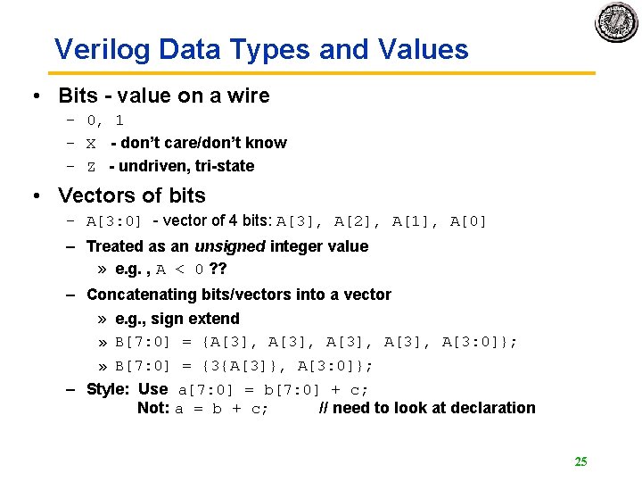
Verilog Data Types and Values • Bits - value on a wire – 0, 1 – X - don’t care/don’t know – Z - undriven, tri-state • Vectors of bits – A[3: 0] - vector of 4 bits: A[3], A[2], A[1], A[0] – Treated as an unsigned integer value » e. g. , A < 0 ? ? – Concatenating bits/vectors into a vector » e. g. , sign extend » B[7: 0] = {A[3], A[3: 0]}; » B[7: 0] = {3{A[3]}, A[3: 0]}; – Style: Use a[7: 0] = b[7: 0] + c; Not: a = b + c; // need to look at declaration 25

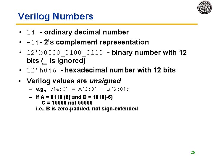
Verilog Numbers • 14 - ordinary decimal number • -14 - 2’s complement representation • 12’b 0000_0110 - binary number with 12 bits (_ is ignored) • 12’h 046 - hexadecimal number with 12 bits • Verilog values are unsigned – e. g. , C[4: 0] = A[3: 0] + B[3: 0]; – if A = 0110 (6) and B = 1010(-6) C = 10000 not 00000 i. e. , B is zero-padded, not sign-extended 26

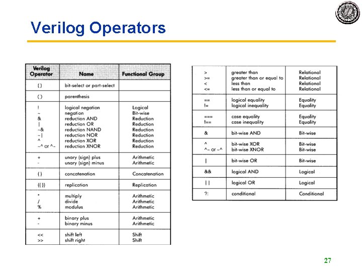
Verilog Operators 27

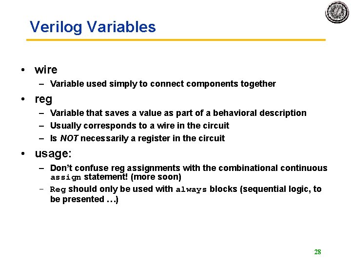
Verilog Variables • wire – Variable used simply to connect components together • reg – Variable that saves a value as part of a behavioral description – Usually corresponds to a wire in the circuit – Is NOT necessarily a register in the circuit • usage: – Don’t confuse reg assignments with the combinational continuous assign statement! (more soon) – Reg should only be used with always blocks (sequential logic, to be presented …) 28

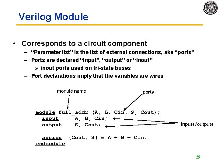
Verilog Module • Corresponds to a circuit component – “Parameter list” is the list of external connections, aka “ports” – Ports are declared “input”, “output” or “inout” » inout ports used on tri-state buses – Port declarations imply that the variables are wires module name ports module full_addr (A, B, Cin, S, Cout); input A, B, Cin; output S, Cout; inputs/outputs assign {Cout, S} = A + B + Cin; endmodule 29

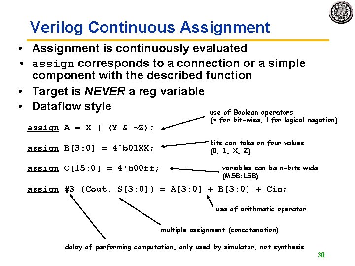
Verilog Continuous Assignment • Assignment is continuously evaluated • assign corresponds to a connection or a simple component with the described function • Target is NEVER a reg variable • Dataflow style use of Boolean operators assign A = X | (Y & ~Z); assign B[3: 0] = 4'b 01 XX; assign C[15: 0] = 4'h 00 ff; (~ for bit-wise, ! for logical negation) bits can take on four values (0, 1, X, Z) variables can be n-bits wide (MSB: LSB) assign #3 {Cout, S[3: 0]} = A[3: 0] + B[3: 0] + Cin; use of arithmetic operator multiple assignment (concatenation) delay of performing computation, only used by simulator, not synthesis 30

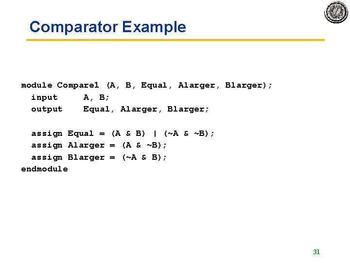
Comparator Example module Compare 1 (A, B, Equal, Alarger, Blarger); input A, B; output Equal, Alarger, Blarger; assign Equal = (A & B) | (~A & ~B); assign Alarger = (A & ~B); assign Blarger = (~A & B); endmodule 31

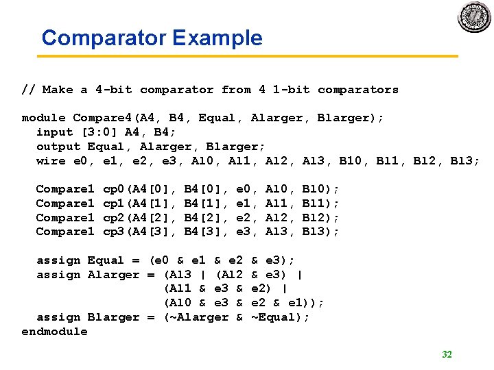
Comparator Example // Make a 4 -bit comparator from 4 1 -bit comparators module Compare 4(A 4, B 4, Equal, Alarger, Blarger); input [3: 0] A 4, B 4; output Equal, Alarger, Blarger; wire e 0, e 1, e 2, e 3, Al 0, Al 1, Al 2, Al 3, B 10, Bl 1, Bl 2, Bl 3; Compare 1 cp 0(A 4[0], cp 1(A 4[1], cp 2(A 4[2], cp 3(A 4[3], B 4[0], B 4[1], B 4[2], B 4[3], e 0, e 1, e 2, e 3, assign Equal = (e 0 & e 1 & e 2 assign Alarger = (Al 3 | (Al 2 (Al 1 & e 3 & (Al 0 & e 3 & assign Blarger = (~Alarger & endmodule Al 0, Al 1, Al 2, Al 3, Bl 0); Bl 1); Bl 2); Bl 3); & e 3); & e 3) | e 2 & e 1)); ~Equal); 32

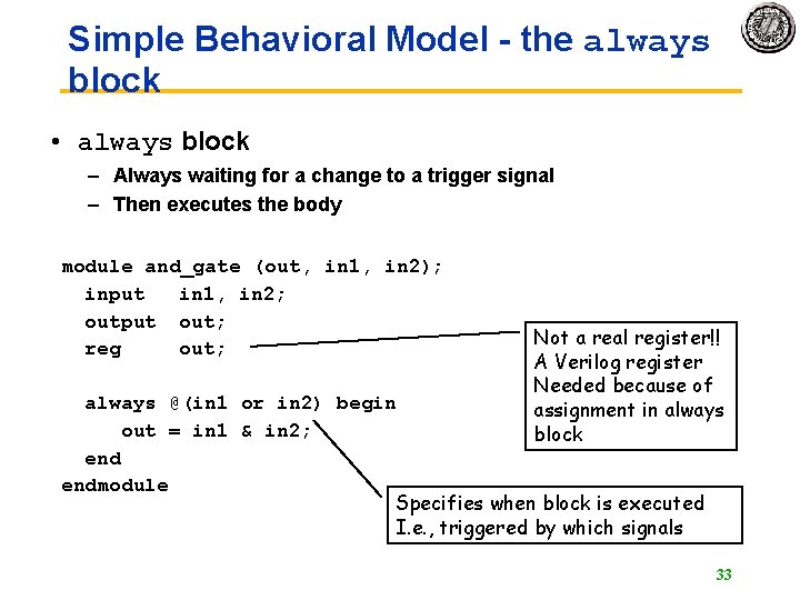
Simple Behavioral Model - the always block • always block – Always waiting for a change to a trigger signal – Then executes the body module and_gate (out, in 1, in 2); input in 1, in 2; output out; reg out; Not a real register!! A Verilog register Needed because of assignment in always block always @(in 1 or in 2) begin out = in 1 & in 2; endmodule Specifies when block is executed I. e. , triggered by which signals 33

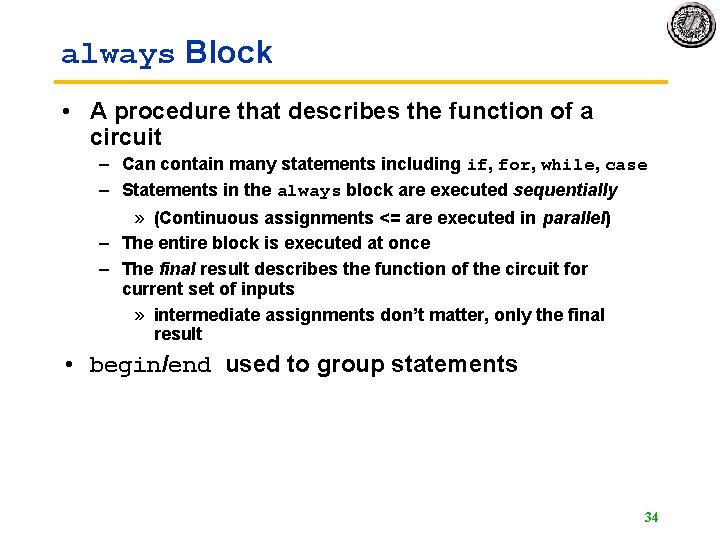
always Block • A procedure that describes the function of a circuit – Can contain many statements including if, for, while, case – Statements in the always block are executed sequentially » (Continuous assignments <= are executed in parallel) – The entire block is executed at once – The final result describes the function of the circuit for current set of inputs » intermediate assignments don’t matter, only the final result • begin/end used to group statements 34

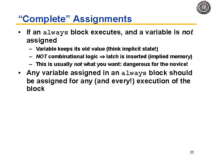
“Complete” Assignments • If an always block executes, and a variable is not assigned – Variable keeps its old value (think implicit state!) – NOT combinational logic latch is inserted (implied memory) – This is usually not what you want: dangerous for the novice! • Any variable assigned in an always block should be assigned for any (and every!) execution of the block 35

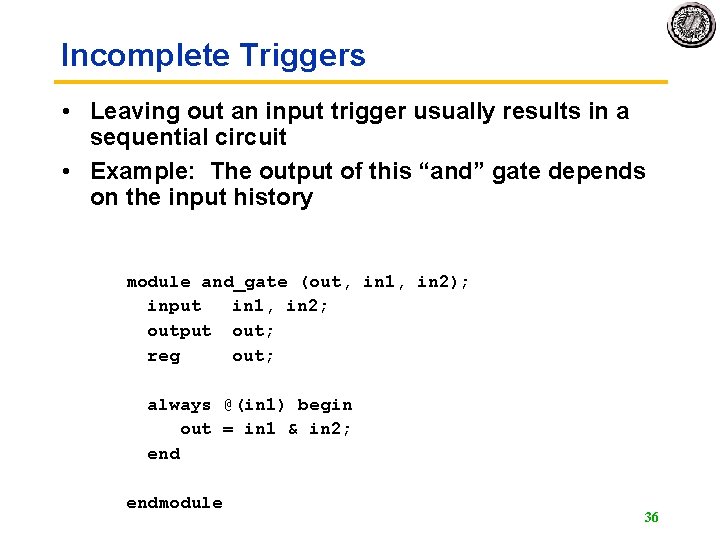
Incomplete Triggers • Leaving out an input trigger usually results in a sequential circuit • Example: The output of this “and” gate depends on the input history module and_gate (out, in 1, in 2); input in 1, in 2; output out; reg out; always @(in 1) begin out = in 1 & in 2; endmodule 36

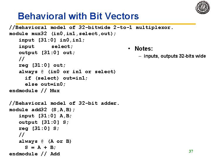
Behavioral with Bit Vectors //Behavioral model of 32 -bitwide 2 -to-1 multiplexor. module mux 32 (in 0, in 1, select, out); input [31: 0] in 0, in 1; input select; • Notes: output [31: 0] out; – inputs, outputs 32 -bits wide // reg [31: 0] out; always @ (in 0 or in 1 or select) if (select) out=in 1; else out=in 0; endmodule // Mux //Behavioral model of 32 -bit adder. module add 32 (S, A, B); input [31: 0] A, B; output [31: 0] S; reg [31: 0] S; // always @ (A or B) S = A + B; endmodule // Add 37

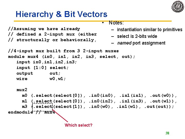
Hierarchy & Bit Vectors • Notes: //Assuming we have already // defined a 2 -input mux (either // structurally or behaviorally, – instantiation similar to primitives – select is 2 -bits wide – named port assignment //4 -input mux built from 3 2 -input muxes module mux 4 (in 0, in 1, in 2, in 3, select, out); input in 0, in 1, in 2, in 3; input [1: 0] select; output out; wire w 0, w 1; mux 2 m 0 (. select(select[0]), . in 0(in 0), . in 1(in 1), . out(w 0)), m 1 (. select(select[0]), . in 0(in 2), . in 1(in 3), . out(w 1)), m 3 (. select(select[1]), . in 0(w 0), . in 1(w 1), . out(out)); endmodule // mux 4 Which select? 38

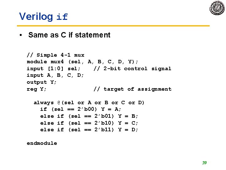
Verilog if • Same as C if statement // Simple 4 -1 mux module mux 4 (sel, A, B, C, D, Y); input [1: 0] sel; // 2 -bit control signal input A, B, C, D; output Y; reg Y; // target of assignment always @(sel or A or B or C or D) if (sel == 2’b 00) Y = A; else if (sel == 2’b 01) Y = B; else if (sel == 2’b 10) Y = C; else if (sel == 2’b 11) Y = D; endmodule 39

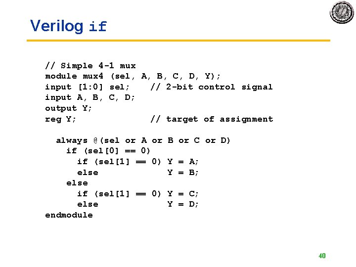
Verilog if // Simple 4 -1 mux module mux 4 (sel, A, B, C, D, Y); input [1: 0] sel; // 2 -bit control signal input A, B, C, D; output Y; reg Y; // target of assignment always @(sel or A or if (sel[0] == 0) if (sel[1] == 0) else endmodule B or C or D) Y = A; Y = B; Y = C; Y = D; 40

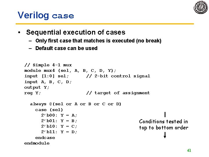
Verilog case • Sequential execution of cases – Only first case that matches is executed (no break) – Default case can be used // Simple 4 -1 mux module mux 4 (sel, A, B, C, D, Y); input [1: 0] sel; // 2 -bit control signal input A, B, C, D; output Y; reg Y; // target of assignment always @(sel case (sel) 2’b 00: Y 2’b 01: Y 2’b 10: Y 2’b 11: Y endcase endmodule or A or B or C or D) = = A; B; C; D; Conditions tested in top to bottom order 41

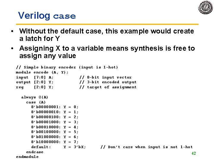
Verilog case • Without the default case, this example would create a latch for Y • Assigning X to a variable means synthesis is free to assign any value // Simple binary encoder module encode (A, Y); input [7: 0] A; output [2: 0] Y; reg [2: 0] Y; always @(A) case (A) 8’b 00000001: 8’b 00000010: 8’b 00000100: 8’b 00001000: 8’b 00010000: 8’b 00100000: 8’b 01000000: 8’b 10000000: default: endcase endmodule Y Y Y Y Y = = = = = (input is 1 -hot) // 8 -bit input vector // 3 -bit encoded output // target of assignment 0; 1; 2; 3; 4; 5; 6; 7; 3’b. X; // Don’t care when input is not 1 -hot 42

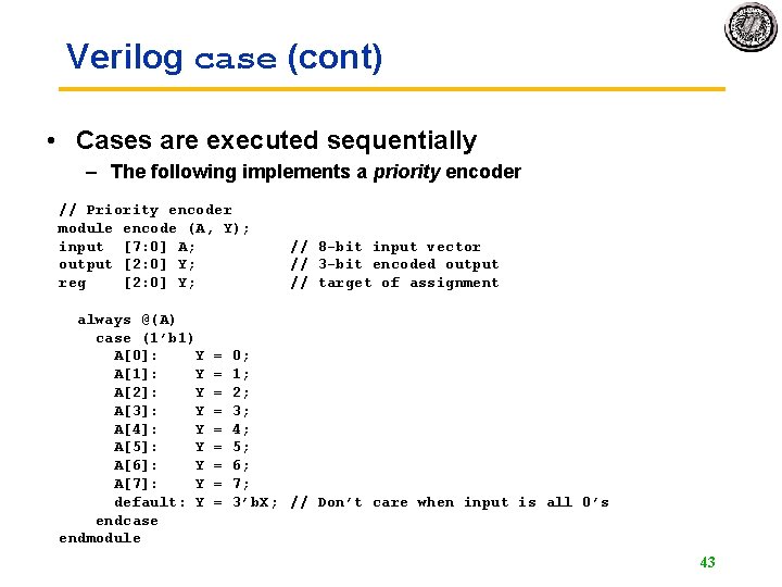
Verilog case (cont) • Cases are executed sequentially – The following implements a priority encoder // Priority encoder module encode (A, Y); input [7: 0] A; output [2: 0] Y; reg [2: 0] Y; always @(A) case (1’b 1) A[0]: Y A[1]: Y A[2]: Y A[3]: Y A[4]: Y A[5]: Y A[6]: Y A[7]: Y default: Y endcase endmodule = = = = = // 8 -bit input vector // 3 -bit encoded output // target of assignment 0; 1; 2; 3; 4; 5; 6; 7; 3’b. X; // Don’t care when input is all 0’s 43

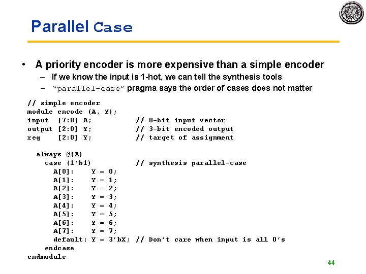
Parallel Case • A priority encoder is more expensive than a simple encoder – If we know the input is 1 -hot, we can tell the synthesis tools – “parallel-case” pragma says the order of cases does not matter // simple encoder module encode (A, Y); input [7: 0] A; output [2: 0] Y; reg [2: 0] Y; always @(A) case (1’b 1) A[0]: Y A[1]: Y A[2]: Y A[3]: Y A[4]: Y A[5]: Y A[6]: Y A[7]: Y default: Y endcase endmodule // 8 -bit input vector // 3 -bit encoded output // target of assignment // synthesis parallel-case = = = = = 0; 1; 2; 3; 4; 5; 6; 7; 3’b. X; // Don’t care when input is all 0’s 44

Verilog casex • Like case, but cases can include ‘X’ – X bits not used when evaluating the cases – In other words, you don’t care about those bits! 45
![casex Example Priority encoder module encode A valid Y input 7 0 A casex Example // Priority encoder module encode (A, valid, Y); input [7: 0] A;](https://slidetodoc.com/presentation_image_h/0da6a8610b4bf26dcd462e92d9514fd1/image-46.jpg)
casex Example // Priority encoder module encode (A, valid, Y); input [7: 0] A; // 8 -bit input vector output [2: 0] Y; // 3 -bit encoded output valid; // Asserted when an input is not all 0’s reg [2: 0] Y; // target of assignment reg valid; always @(A) begin valid = 1; casex (A) 8’b. XXXXXXX 1: Y = 8’b. XXXXXX 10: Y = 8’b. XXXXX 100: Y = 8’b. XXXX 1000: Y = 8’b. XXX 10000: Y = 8’b. XX 100000: Y = 8’b. X 1000000: Y = 8’b 10000000: Y = default: begin valid = 0; Y = 3’b. X; // endcase endmodule 0; 1; 2; 3; 4; 5; 6; 7; Don’t care when input is all 0’s 46

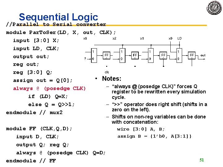
Sequential Logic //Parallel to Serial converter module Par. To. Ser(LD, X, out, CLK); input [3: 0] X; input LD, CLK; output out; reg [3: 0] Q; • Notes: assign out = Q[0]; – “always @ (posedge CLK)” forces Q always @ (posedge CLK) register to be rewritten every simulation if (LD) Q=X; cycle. – “>>” operator does right shift (shifts in a else Q = Q>>1; zero on the left). endmodule // mux 2 module FF (CLK, Q, D); input D, CLK; output Q; reg Q; always @ (posedge CLK) Q=D; endmodule // FF – Shifts on non-reg variables can be done with concatenation: wire [3: 0] A, B; assign B = {1’b 0, A[3: 1]} 51

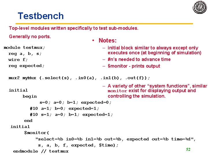
Testbench Top-level modules written specifically to test sub-modules. Generally no ports. module testmux; reg a, b, s; wire f; reg expected; • Notes: – initial block similar to always except only executes once (at beginning of simulation) – #n’s needed to advance time – $monitor - prints output mux 2 my. Mux (. select(s), . in 0(a), . in 1(b), . out(f)); – A variety of other “system functions”, similar initial monitor exist for displaying output and begin controlling the simulation. s=0; a=0; b=1; expected=0; #10 a=1; b=0; expected=1; #10 s=1; a=0; b=1; expected=1; end initial $monitor( "select=%b in 0=%b in 1=%b out=%b, expected out=%b time=%d", s, a, b, f, expected, $time); 52 endmodule // testmux

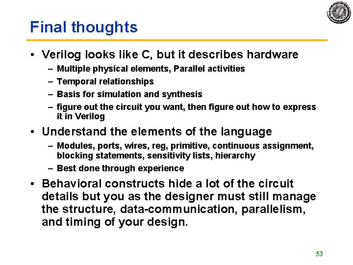
Final thoughts • Verilog looks like C, but it describes hardware – – Multiple physical elements, Parallel activities Temporal relationships Basis for simulation and synthesis figure out the circuit you want, then figure out how to express it in Verilog • Understand the elements of the language – Modules, ports, wires, reg, primitive, continuous assignment, blocking statements, sensitivity lists, hierarchy – Best done through experience • Behavioral constructs hide a lot of the circuit details but you as the designer must still manage the structure, data-communication, parallelism, and timing of your design. 53