EECS 150 Components and Design Techniques for Digital




- Slides: 46

EECS 150 - Components and Design Techniques for Digital Systems Lec 22 – Sequential Logic - Advanced David Culler Electrical Engineering and Computer Sciences University of California, Berkeley http: //www. eecs. berkeley. edu/~culler http: //inst. eecs. berkeley. edu/~cs 150

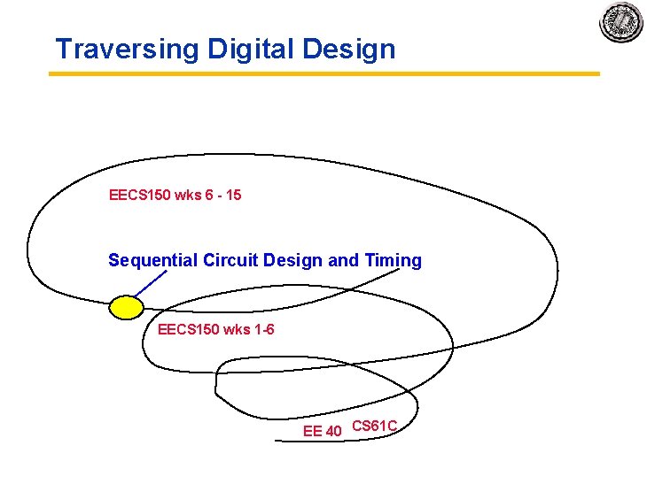
Traversing Digital Design EECS 150 wks 6 - 15 Sequential Circuit Design and Timing EECS 150 wks 1 -6 EE 40 CS 61 C

RTL & ISA

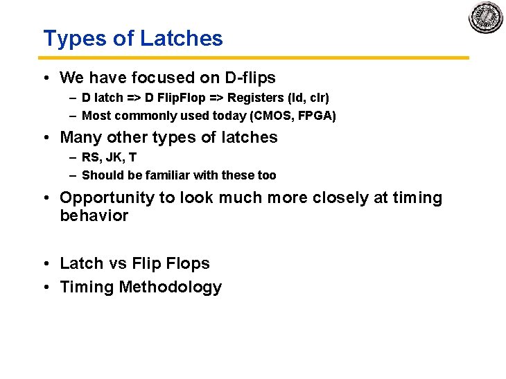
Types of Latches • We have focused on D-flips – D latch => D Flip. Flop => Registers (ld, clr) – Most commonly used today (CMOS, FPGA) • Many other types of latches – RS, JK, T – Should be familiar with these too • Opportunity to look much more closely at timing behavior • Latch vs Flip Flops • Timing Methodology

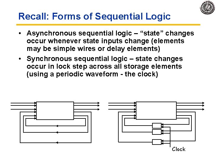
Recall: Forms of Sequential Logic • Asynchronous sequential logic – “state” changes occur whenever state inputs change (elements may be simple wires or delay elements) • Synchronous sequential logic – state changes occur in lock step across all storage elements (using a periodic waveform - the clock) Clock

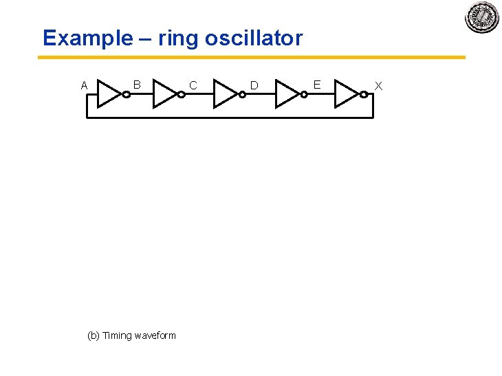
Example – ring oscillator A B (b) Timing waveform C D E X

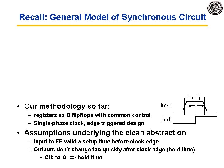
Recall: General Model of Synchronous Circuit Tsu Th • Our methodology so far: – registers as D flipflops with common control – Single-phase clock, edge triggered design input clock • Assumptions underlying the clean abstraction – Input to FF valid a setup time before clock edge – Outputs don’t change too quickly after clock edge (hold time) » Clk-to-Q => hold time

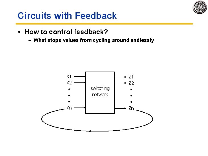
Circuits with Feedback • How to control feedback? – What stops values from cycling around endlessly X 1 X 2 • • • Xn switching network Z 1 Z 2 • • • Zn

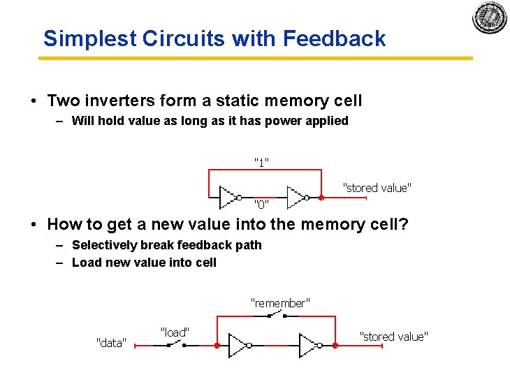
Simplest Circuits with Feedback • Two inverters form a static memory cell – Will hold value as long as it has power applied "1" "stored value" "0" • How to get a new value into the memory cell? – Selectively break feedback path – Load new value into cell "remember" "data" "load" "stored value"

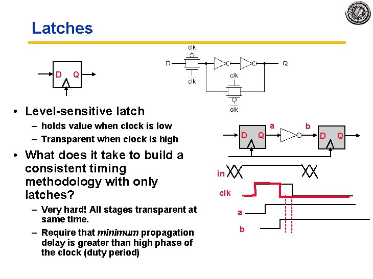
Latches D Q • Level-sensitive latch – holds value when clock is low – Transparent when clock is high • What does it take to build a consistent timing methodology with only latches? – Very hard! All stages transparent at same time. – Require that minimum propagation delay is greater than high phase of the clock (duty period) a D in clk a b Q b D Q

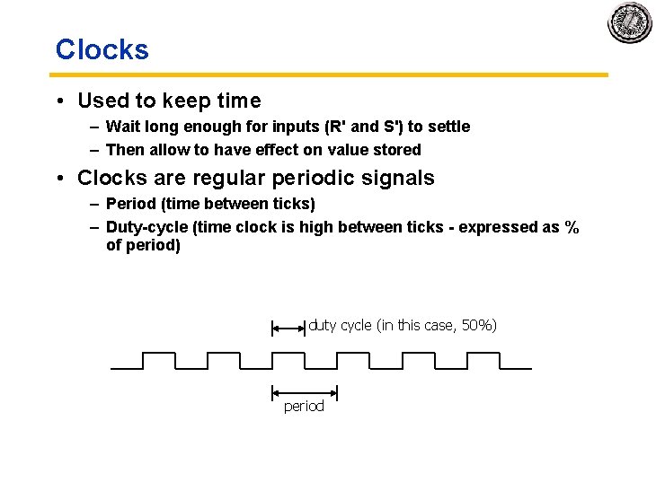
Clocks • Used to keep time – Wait long enough for inputs (R' and S') to settle – Then allow to have effect on value stored • Clocks are regular periodic signals – Period (time between ticks) – Duty-cycle (time clock is high between ticks - expressed as % of period) duty cycle (in this case, 50%) period

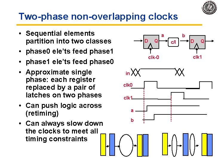
Two-phase non-overlapping clocks • Sequential elements partition into two classes • phase 0 ele’ts feed phase 1 • phase 1 ele’ts feed phase 0 • Approximate single phase: each register replaced by a pair of latches on two phases • Can push logic across (retiming) • Can always slow down the clocks to meet all timing constraints a D Q clk-0 in clk 0 clk 1 a b b c/l D Q clk 1

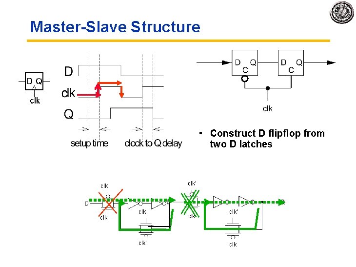
Master-Slave Structure • Construct D flipflop from two D latches clk’ clk

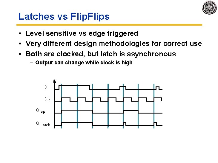
Latches vs Flips • Level sensitive vs edge triggered • Very different design methodologies for correct use • Both are clocked, but latch is asynchronous – Output can change while clock is high D Clk Q Q FF Latch

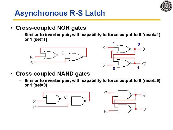
Asynchronous R-S Latch • Cross-coupled NOR gates – Similar to inverter pair, with capability to force output to 0 (reset=1) or 1 (set=1) R 1 0 Q Q R S S • Cross-coupled NAND gates 0 1 Q' – Similar to inverter pair, with capability to force output to 0 (reset=0) or 1 (set=0) S' R' Q Q'

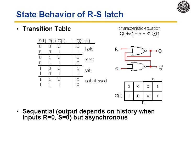
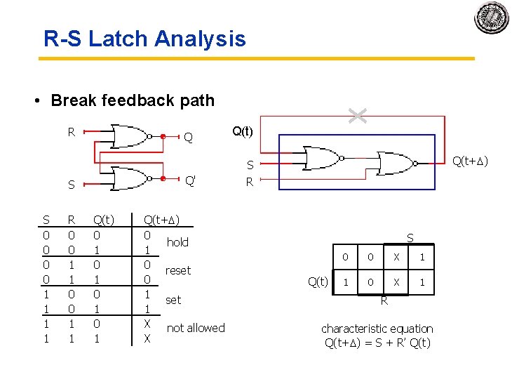
State Behavior of R-S latch • Transition Table S(t) 0 0 1 1 R(t) 0 0 1 1 Q(t) 0 1 0 1 characteristic equation Q(t+ ) = S + R’ Q(t) Q(t+ ) 0 hold 1 0 reset 0 1 set 1 X not allowed X R Q S Q' S Q(t) 0 0 X 1 1 0 X 1 R • Sequential (output depends on history when inputs R=0, S=0) but asynchronous

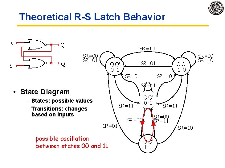
Theoretical R-S Latch Behavior R S Q Q' SR=10 SR=01 Q Q' 0 1 SR=01 Q Q' 1 0 SR=11 • State Diagram – States: possible values – Transitions: changes based on inputs SR=11 SR=01 possible oscillation between states 00 and 11 Q Q' 0 0 SR=11 SR=00 SR=10 Q Q' 1 1 SR=00 SR=10

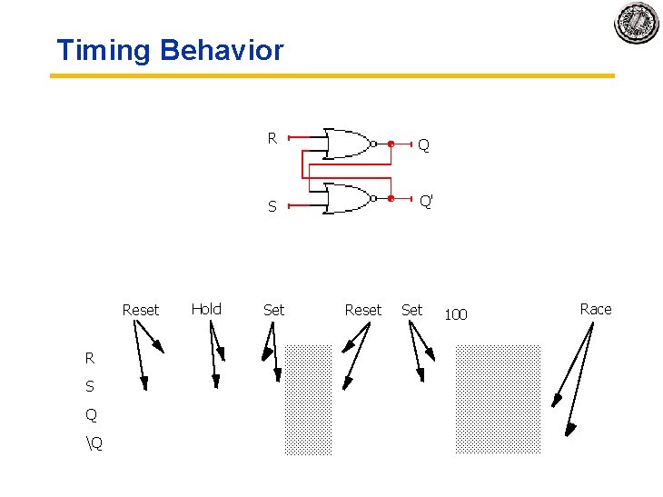
Timing Behavior Reset R S Q Q Hold R Q S Q' Set Reset Set 100 Race

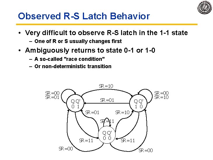
Observed R-S Latch Behavior • Very difficult to observe R-S latch in the 1 -1 state – One of R or S usually changes first • Ambiguously returns to state 0 -1 or 1 -0 – A so-called "race condition" – Or non-deterministic transition SR=10 SR=01 Q Q' 0 1 SR=01 Q Q' 1 0 SR=11 SR=00 Q Q' 0 0 SR=11 SR=00 SR=10

R-S Latch Analysis • Break feedback path R Q Q(t) Q(t+ ) S Q' S S 0 0 1 1 R 0 0 1 1 Q(t) 0 1 0 1 Q(t+ ) 0 hold 1 0 reset 0 1 set 1 X not allowed X R S Q(t) 0 0 X 1 1 0 X 1 R characteristic equation Q(t+ ) = S + R’ Q(t)

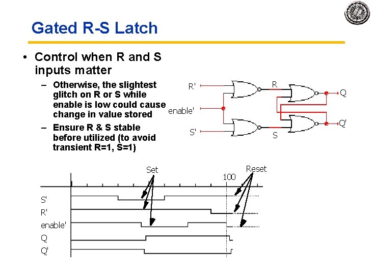
Gated R-S Latch • Control when R and S inputs matter – Otherwise, the slightest R' glitch on R or S while enable is low could cause enable' change in value stored – Ensure R & S stable S' before utilized (to avoid transient R=1, S=1) Set S' R' enable' Q Q' R Q Q' S 100 Reset

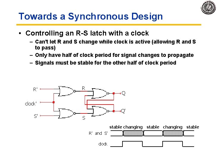
Towards a Synchronous Design • Controlling an R-S latch with a clock – Can't let R and S change while clock is active (allowing R and S to pass) – Only have half of clock period for signal changes to propagate – Signals must be stable for the other half of clock period R' R Q clock' S' Q' S stable changing stable R' and S' clock

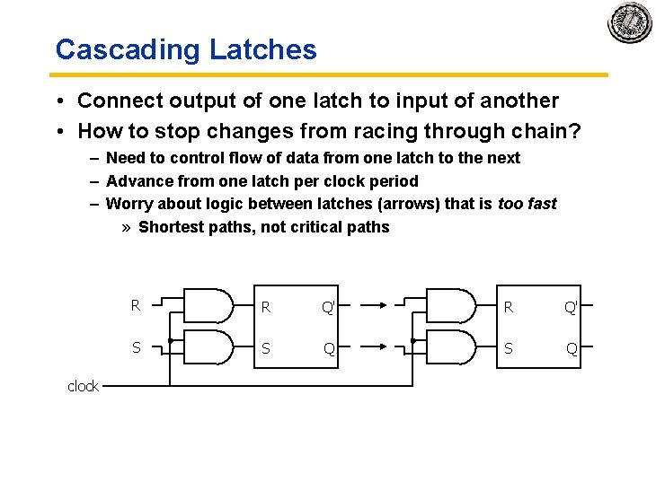
Cascading Latches • Connect output of one latch to input of another • How to stop changes from racing through chain? – Need to control flow of data from one latch to the next – Advance from one latch per clock period – Worry about logic between latches (arrows) that is too fast » Shortest paths, not critical paths clock R R Q' S S Q

Announcements • • • Guest Lecture, Nov 29, Dr. Robert Iannucci, CTO Nokia Sarah Lecture on Testing Methodology Thurs. HW out tonight, due before Break Lab lecture covers “final point” Wireless CP this week Next week TAs will do extended office hours M-W rather than formal Final Check off week 14 No Class Dec 6. Final report Friday Dec. 7. Sign up for 10 min slots – 5 min presentation, 5 min Q&A – Arrive 20 mins before scheduled slot to set up

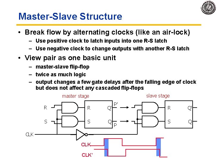
Master-Slave Structure • Break flow by alternating clocks (like an air-lock) – Use positive clock to latch inputs into one R-S latch – Use negative clock to change outputs with another R-S latch • View pair as one basic unit – master-slave flip-flop – twice as much logic – output changes a few gate delays after the falling edge of clock but does not affect any cascaded flip-flops slave stage master stage R R Q' S S Q CLK CLK’ P' P R Q' S Q

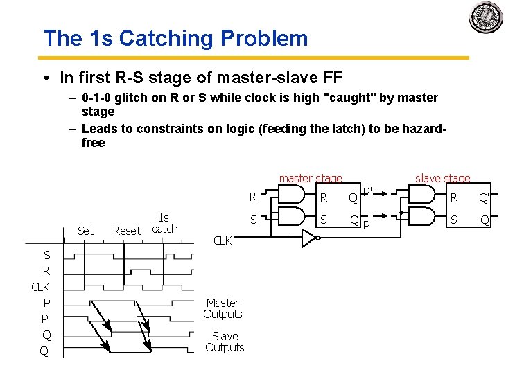
The 1 s Catching Problem • In first R-S stage of master-slave FF – 0 -1 -0 glitch on R or S while clock is high "caught" by master stage – Leads to constraints on logic (feeding the latch) to be hazardfree slave stage master stage Set S R CLK P P' Q Q' Reset 1 s catch CLK Master Outputs Slave Outputs R R Q' S S Q P' P R Q' S Q

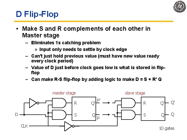
D Flip-Flop • Make S and R complements of each other in Master stage – Eliminates 1 s catching problem » Input only needs to settle by clock edge – Can't just hold previous value (must have new value ready every clock period) – Value of D just before clock goes low is what is stored in flipflop – Can make R-S flip-flop by adding logic to make D = S + R' Q slave stage master stage D CLK R Q' S Q P' P R Q' Q' S Q Q 10 gates

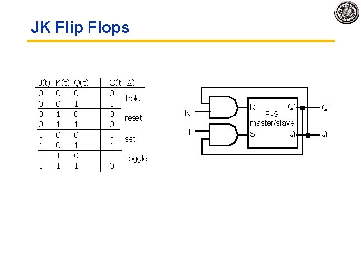
JK Flip Flops J(t) 0 0 1 1 K(t) 0 0 1 1 Q(t) 0 1 0 1 Q(t+ ) 0 hold 1 0 reset 0 1 set 1 1 toggle 0 K J R Q’ R-S master/slave S Q Q’ Q

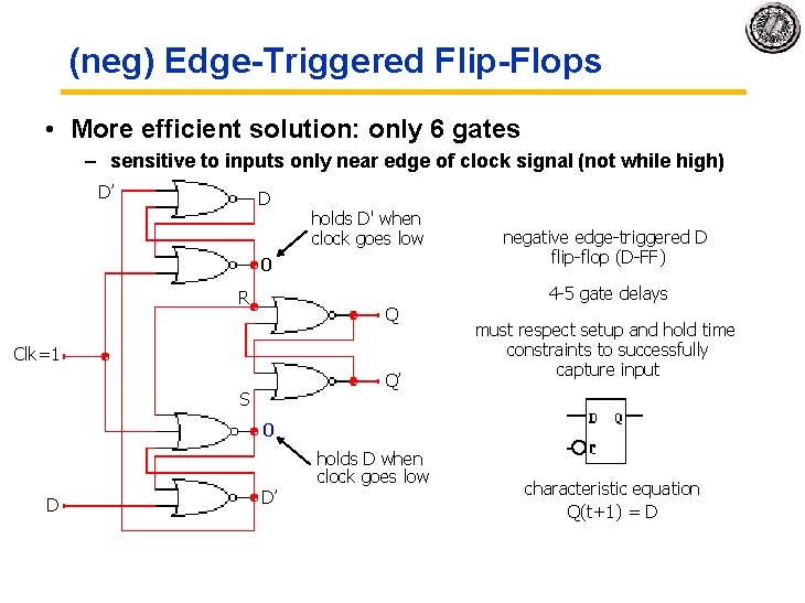
(neg) Edge-Triggered Flip-Flops • More efficient solution: only 6 gates – sensitive to inputs only near edge of clock signal (not while high) D’ D holds D' when clock goes low 0 R Q Clk=1 Q’ S negative edge-triggered D flip-flop (D-FF) 4 -5 gate delays must respect setup and hold time constraints to successfully capture input 0 holds D when clock goes low D D’ characteristic equation Q(t+1) = D

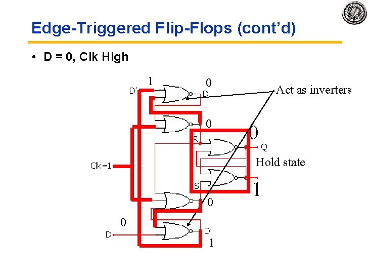
Edge-Triggered Flip-Flops (cont’d) • D = 0, Clk High D’ 1 0 D’ 0 R 0 Q Hold state Clk=1 S D 0 0 D Act as inverters D D’ 1 1

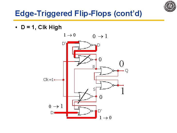
Edge-Triggered Flip-Flops (cont’d) • D = 1, Clk High 11 ® 0 0® 1 D’ D D’ 0 R 0 Clk=1 S D 0 0 ® 01 D D’ 11 ® 0 1 Q

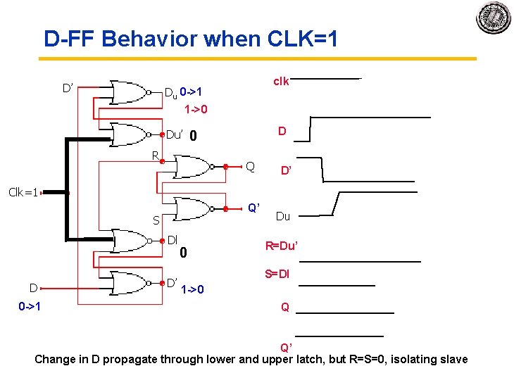
D-FF Behavior when CLK=1 D’ clk Du 0 ->1 1 ->0 Du’ D 0 R Q D’ Clk=1 Q’ S Dl D 0 ->1 D’ 0 Du R=Du’ S=Dl 1 ->0 Q Q’ Change in D propagate through lower and upper latch, but R=S=0, isolating slave

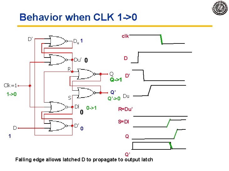
Behavior when CLK 1 ->0 D’ clk Du 1 Du’ R Q Q->1 Clk=1 1 ->0 1 D’ Q’ Du Q’->0 S Dl D D 0 D’ 0 0 ->1 R=Du’ S=Dl 0 Q Q’ Falling edge allows latched D to propagate to output latch

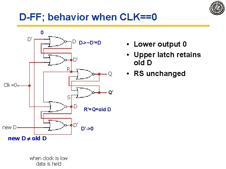
D-FF; behavior when CLK==0 0 D’ D D->~D’=D D’ R Q Clk=0 Q’ S D D’ new D old D when clock is low data is held R’=Q=old D D’->0 • Lower output 0 • Upper latch retains old D • RS unchanged

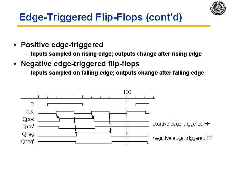
Edge-Triggered Flip-Flops (cont’d) • Positive edge-triggered – Inputs sampled on rising edge; outputs change after rising edge • Negative edge-triggered flip-flops – Inputs sampled on falling edge; outputs change after falling edge 100 D CLK Qpos' Qneg' positive edge-triggered FF negative edge-triggered FF

Timing Methodologies • Rules for interconnecting components and clocks – Guarantee properation of system when strictly followed • Approach depends on building blocks used for memory elements – Focus on systems with edge-triggered flip-flops » Found in programmable logic devices – Many custom integrated circuits focus on level-sensitive latches • Basic rules for correct timing: – (1) Correct inputs, with respect to time, are provided to the flip-flops – (2) No flip-flop changes state more than once per clocking event

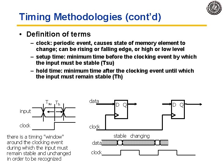
Timing Methodologies (cont’d) • Definition of terms – clock: periodic event, causes state of memory element to change; can be rising or falling edge, or high or low level – setup time: minimum time before the clocking event by which the input must be stable (Tsu) – hold time: minimum time after the clocking event until which the input must remain stable (Th) Tsu Th data D Q input clock there is a timing "window" around the clocking event during which the input must remain stable and unchanged in order to be recognized clock stable changing data clock D Q

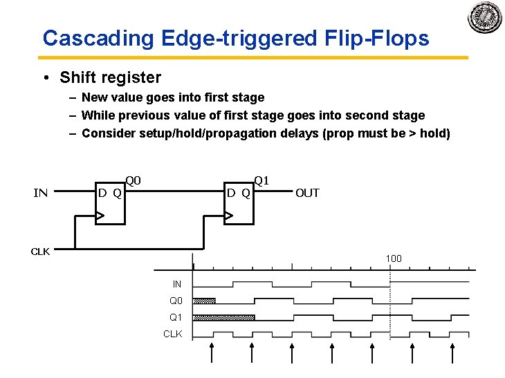
Cascading Edge-triggered Flip-Flops • Shift register – New value goes into first stage – While previous value of first stage goes into second stage – Consider setup/hold/propagation delays (prop must be > hold) IN D Q Q 0 D Q CLK Q 1 OUT 100 IN Q 0 Q 1 CLK

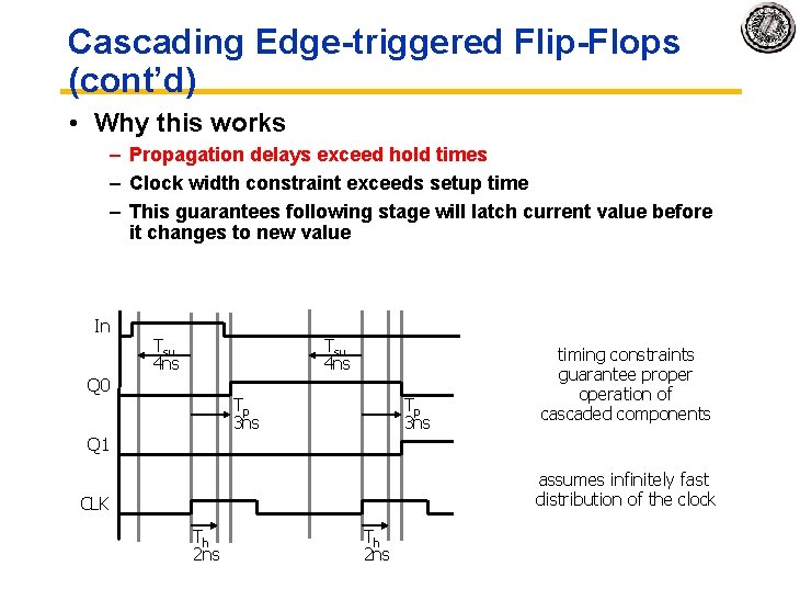
Cascading Edge-triggered Flip-Flops (cont’d) • Why this works – Propagation delays exceed hold times – Clock width constraint exceeds setup time – This guarantees following stage will latch current value before it changes to new value In Tsu 4 ns Q 0 Tp 3 ns timing constraints guarantee properation of cascaded components Q 1 assumes infinitely fast distribution of the clock CLK Th 2 ns

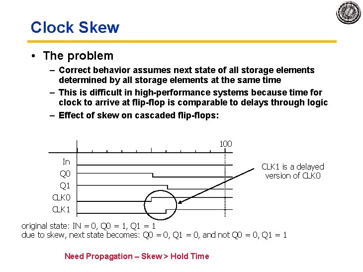
Clock Skew • The problem – Correct behavior assumes next state of all storage elements determined by all storage elements at the same time – This is difficult in high-performance systems because time for clock to arrive at flip-flop is comparable to delays through logic – Effect of skew on cascaded flip-flops: 100 In Q 0 CLK 1 is a delayed version of CLK 0 Q 1 CLK 0 CLK 1 original state: IN = 0, Q 0 = 1, Q 1 = 1 due to skew, next state becomes: Q 0 = 0, Q 1 = 0, and not Q 0 = 0, Q 1 = 1 Need Propagation – Skew > Hold Time

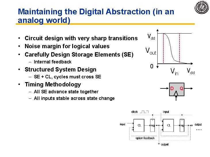
Maintaining the Digital Abstraction (in an analog world) • Circuit design with very sharp transitions • Noise margin for logical values • Carefully Design Storage Elements (SE) – Internal feedback • Structured System Design – SE + CL, cycles must cross SE • Timing Methodology – All SE advance state together – All inputs stable across state change Vdd Vout 0 Vin D Vdd Q

Where does this breakdown? • Interfacing to the physical world • Can’t tell it “not to change near the clock edge” Digital Abstraction

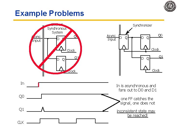
Example Problems Clocked Synchronous System Async Input D Q Synchronizer Q 0 Async Input D Q Clock D Q Q 1 Clock In Q 0 Q 1 CLK Q 0 D Q Q 1 D Q Clock In is asynchronous and fans out to D 0 and D 1 one FF catches the signal, one does not inconsistent state may be reached!

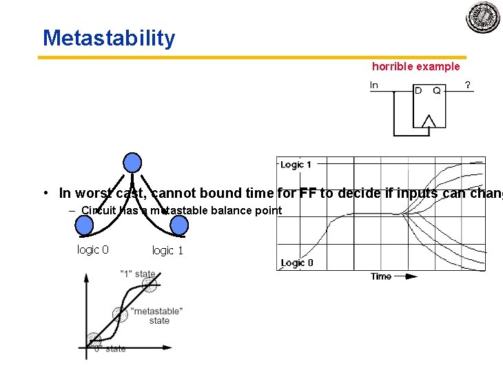
Metastability horrible example • In worst cast, cannot bound time for FF to decide if inputs can chang – Circuit has a metastable balance point logic 0 logic 1

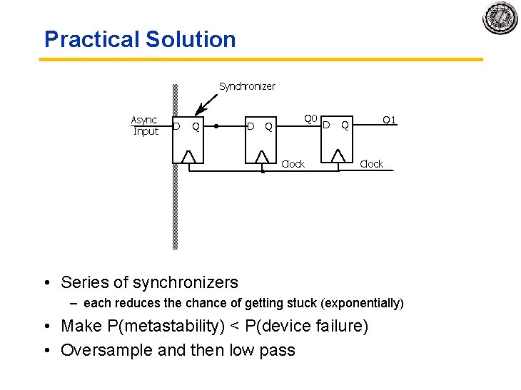
Practical Solution Synchronizer Async Input D Q Q 0 Clock D Q 1 Q Clock • Series of synchronizers – each reduces the chance of getting stuck (exponentially) • Make P(metastability) < P(device failure) • Oversample and then low pass

Metastability throughout the ages Buridan, Jean (1300 -58), French Scholastic philosopher, who held a theory of determinism, contending that the will must choose the greater good. Born in Bethune, he was educated at the University of Paris, where he studied with the English Scholastic philosopher William of Ocham. After his studies were completed, he was appointed professor of philosophy, and later rector, at the same university. Buridan is traditionally but probably incorrectly associated with a philosophical dilemma of moral choice called "Buridan's ass. " In the problem an ass starves to death between two alluring bundles of hay because it does not have the will to decide which one to eat. Didn’t take EECS 150