EECS 150 Components and Design Techniques for Digital
- Slides: 43

EECS 150 - Components and Design Techniques for Digital Systems Lec 13 – Storage: Regs, SRAM, ROM David Culler Electrical Engineering and Computer Sciences University of California, Berkeley http: //www. eecs. berkeley. edu/~culler http: //inst. eecs. berkeley. edu/~cs 150 10 -9 -2007 EECS 150 -Fa 07 Lec 13 -RAM 1

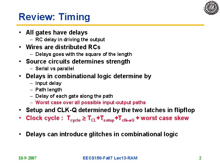
Review: Timing • All gates have delays – RC delay in driving the output • Wires are distributed RCs – Delays goes with the square of the length • Source circuits determines strength – Serial vs parallel • Delays in combinational logic determine by – – Input delay Path length Delay of each gate along the path Worst case over all possible input-output paths • Setup and CLK-Q determined by the two latches in flipflop • Clock cycle : Tcycle TCL+Tsetup+Tclk Q + worst case skew • Delays can introduce glitches in combinational logic 10 -9 -2007 EECS 150 -Fa 07 Lec 13 -RAM 2

Outline • • • Memory concepts Register Files SRAM Access Multiported Memories – FIFOS • ROM, EPROM, FLASH • Relationship to Comb. Logic 10 -9 -2007 EECS 150 -Fa 07 Lec 13 -RAM 3

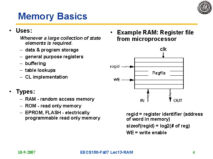
Memory Basics • Uses: Whenever a large collection of state elements is required. – data & program storage – general purpose registers – buffering – table lookups – CL implementation • Example RAM: Register file from microprocessor clk • Types: – RAM - random access memory – ROM - read only memory – EPROM, FLASH - electrically programmable read only memory 10 -9 -2007 regid = register identifier (address of word in memory) sizeof(regid) = log 2(# of reg) WE = write enable EECS 150 -Fa 07 Lec 13 -RAM 4

Examples in your project • • • Local device configuration Registry of other devices Video object store Video object pixel maps FIFOs connecting peripherals to the core Audio storage 10 -9 -2007 EECS 150 -Fa 07 Lec 13 -RAM 5

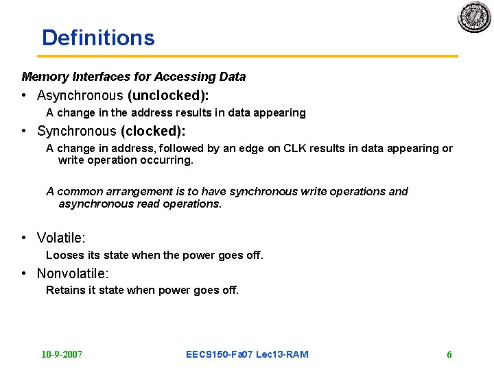
Definitions Memory Interfaces for Accessing Data • Asynchronous (unclocked): A change in the address results in data appearing • Synchronous (clocked): A change in address, followed by an edge on CLK results in data appearing or write operation occurring. A common arrangement is to have synchronous write operations and asynchronous read operations. • Volatile: Looses its state when the power goes off. • Nonvolatile: Retains it state when power goes off. 10 -9 -2007 EECS 150 -Fa 07 Lec 13 -RAM 6

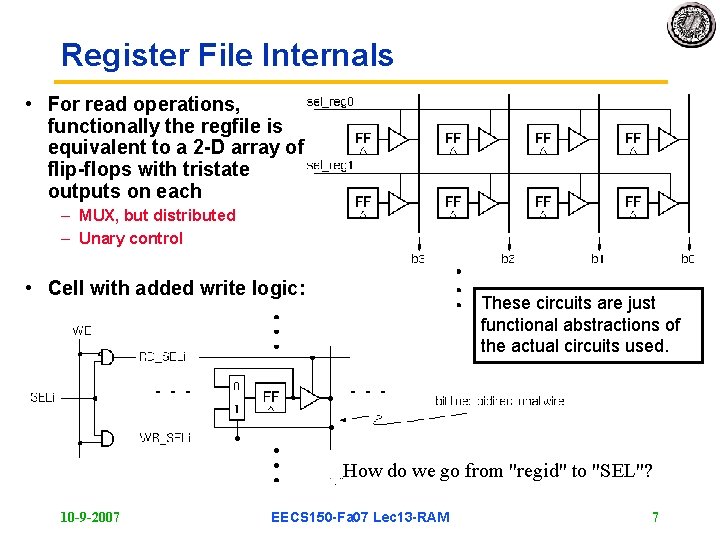
Register File Internals • For read operations, functionally the regfile is equivalent to a 2 -D array of flip-flops with tristate outputs on each – MUX, but distributed – Unary control • Cell with added write logic: These circuits are just functional abstractions of the actual circuits used. How do we go from "regid" to "SEL"? 10 -9 -2007 EECS 150 -Fa 07 Lec 13 -RAM 7

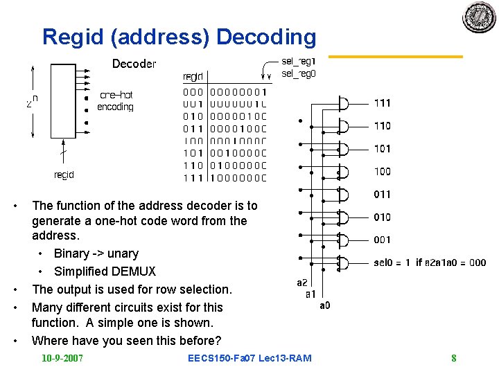
Regid (address) Decoding • • The function of the address decoder is to generate a one-hot code word from the address. • Binary -> unary • Simplified DEMUX The output is used for row selection. Many different circuits exist for this function. A simple one is shown. Where have you seen this before? 10 -9 -2007 EECS 150 -Fa 07 Lec 13 -RAM 8

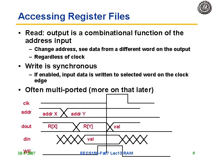
Accessing Register Files • Read: output is a combinational function of the address input – Change address, see data from a different word on the output – Regardless of clock • Write is synchronous – If enabled, input data is written to selected word on the clock edge • Often multi-ported (more on that later) clk addr X dout R[X] din WE 10 -9 -2007 addr Y R[Y] val EECS 150 -Fa 07 Lec 13 -RAM 9

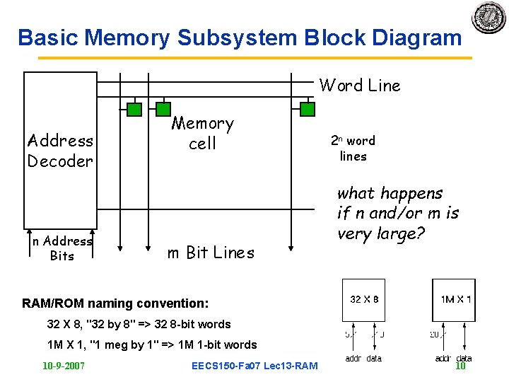
Basic Memory Subsystem Block Diagram Word Line Address Decoder n Address Bits Memory cell m Bit Lines 2 n word lines what happens if n and/or m is very large? RAM/ROM naming convention: 32 X 8, "32 by 8" => 32 8 -bit words 1 M X 1, "1 meg by 1" => 1 M 1 -bit words 10 -9 -2007 EECS 150 -Fa 07 Lec 13 -RAM 10

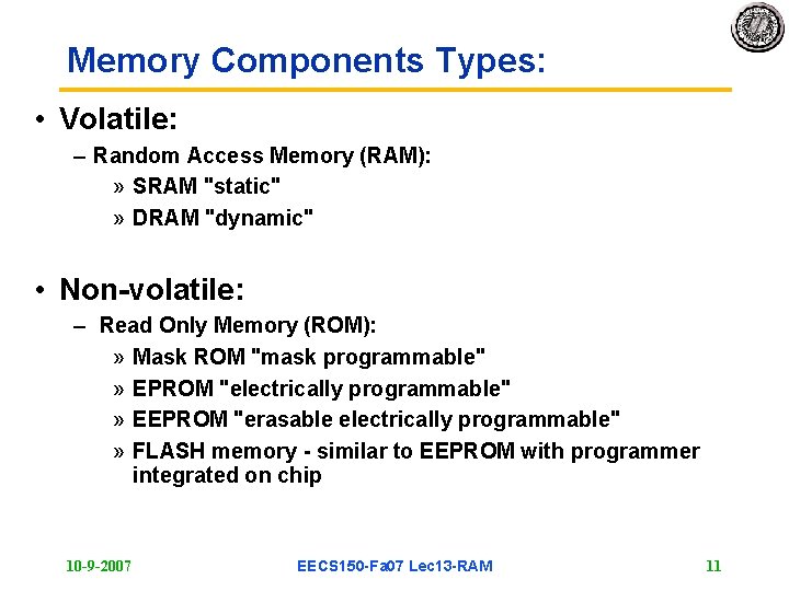
Memory Components Types: • Volatile: – Random Access Memory (RAM): » SRAM "static" » DRAM "dynamic" • Non-volatile: – Read Only Memory (ROM): » Mask ROM "mask programmable" » EPROM "electrically programmable" » EEPROM "erasable electrically programmable" » FLASH memory - similar to EEPROM with programmer integrated on chip 10 -9 -2007 EECS 150 -Fa 07 Lec 13 -RAM 11

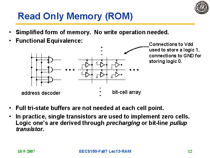
Read Only Memory (ROM) • Simplified form of memory. No write operation needed. • Functional Equivalence: Connections to Vdd used to store a logic 1, connections to GND for storing logic 0. address decoder bit-cell array • Full tri-state buffers are not needed at each cell point. • In practice, single transistors are used to implement zero cells. Logic one’s are derived through precharging or bit-line pullup transistor. 10 -9 -2007 EECS 150 -Fa 07 Lec 13 -RAM 12

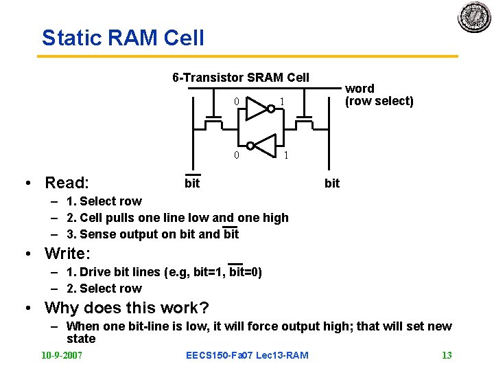
Static RAM Cell 6 -Transistor SRAM Cell 0 0 • Read: word (row select) 1 1 bit – 1. Select row – 2. Cell pulls one line low and one high – 3. Sense output on bit and bit • Write: – 1. Drive bit lines (e. g, bit=1, bit=0) – 2. Select row • Why does this work? – When one bit-line is low, it will force output high; that will set new state 10 -9 -2007 EECS 150 -Fa 07 Lec 13 -RAM 13

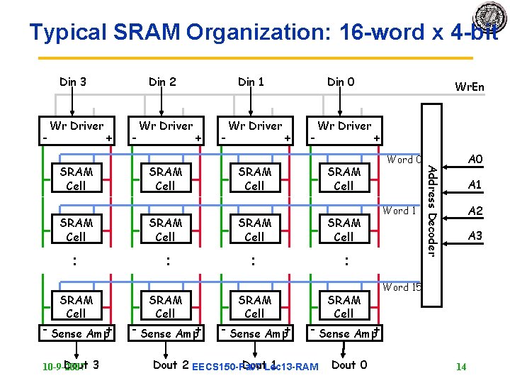
Typical SRAM Organization: 16 -word x 4 -bit Din 3 - Wr Driver Din 2 + + SRAM Cell - Wr Driver Din 0 + - Wr Driver SRAM Cell Wr. En + SRAM Cell SRAM Cell : : SRAM Cell - Sense Amp+ Dout 3 10 -9 -2007 Dout 2 EECS 150 -Fa 07 Dout. Lec 13 -RAM 1 Dout 0 Word 1 A 0 Address Decoder SRAM Cell - Wr Driver Din 1 A 2 A 3 Word 15 14

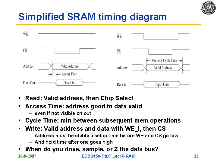
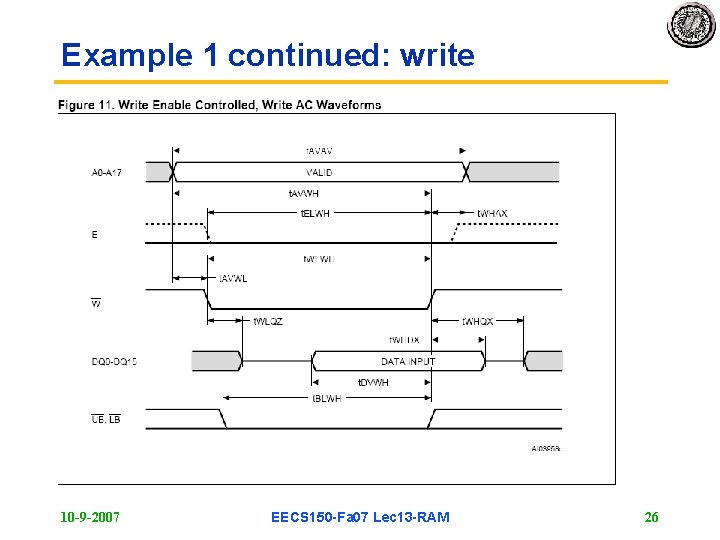
Simplified SRAM timing diagram • Read: Valid address, then Chip Select • Access Time: address good to data valid – even if not visible on out • Cycle Time: min between subsequent mem operations • Write: Valid address and data with WE_l, then CS – Address must be stable a setup time before WE and CS go low – And hold time after one goes high • When do you drive, sample, or Z the data bus? 10 -9 -2007 EECS 150 -Fa 07 Lec 13 -RAM 15

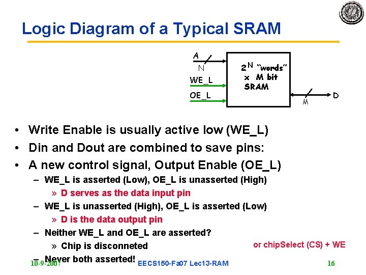
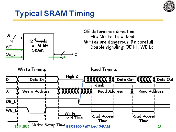
Logic Diagram of a Typical SRAM A N WE_L OE_L 2 N “words” x M bit SRAM M D • Write Enable is usually active low (WE_L) • Din and Dout are combined to save pins: • A new control signal, Output Enable (OE_L) – WE_L is asserted (Low), OE_L is unasserted (High) » D serves as the data input pin – WE_L is unasserted (High), OE_L is asserted (Low) » D is the data output pin – Neither WE_L and OE_L are asserted? or chip. Select (CS) + WE » Chip is disconneted – Never both asserted! EECS 150 -Fa 07 Lec 13 -RAM 16 10 -9 -2007

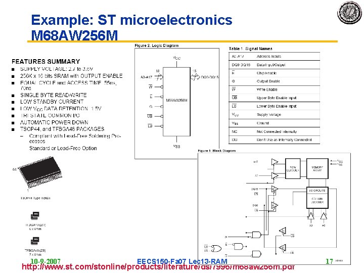
Example: ST microelectronics M 68 AW 256 M 10 -9 -2007 EECS 150 -Fa 07 Lec 13 -RAM http: //www. st. com/stonline/products/literature/ds/7996/m 68 aw 256 m. pdf 17

Administration and Announcements • Thanks for feedback on survey – Slow down – course and lecture – More examples – lecture and lab lecture – Mid term too long • Lab lecture => Pre Lab => Design review => Execute => Check off – You need to pay attention to lab lecture on what to do next while executing current lab. – Do the prelab before lab. The beginning of lab is turn in design review document of current and check off of previous. • Update on lab check offs – 4 days of slip that you can use as needed (but cannot extend into weekend) – Can accepts black box on lab to catch up » Recoup 50% if implement your own within 2 weeks • All homeworks graded. On-line grades available for labs, HWs, and Mid • Solution for current HW will be posted on Friday! 10 -9 -2007 EECS 150 -Fa 07 Lec 13 -RAM 18

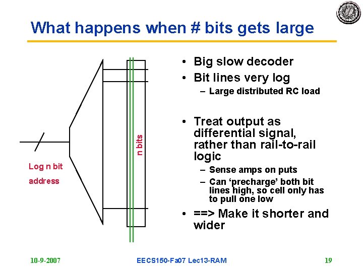
What happens when # bits gets large • Big slow decoder • Bit lines very log n bits – Large distributed RC load Log n bit address • Treat output as differential signal, rather than rail-to-rail logic – Sense amps on puts – Can ‘precharge’ both bit lines high, so cell only has to pull one low • ==> Make it shorter and wider 10 -9 -2007 EECS 150 -Fa 07 Lec 13 -RAM 19

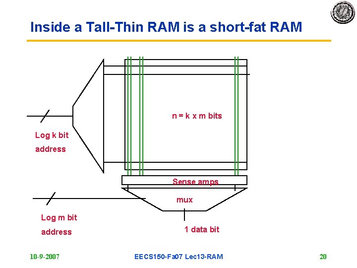
Inside a Tall-Thin RAM is a short-fat RAM n = k x m bits Log k bit address Sense amps mux Log m bit address 10 -9 -2007 1 data bit EECS 150 -Fa 07 Lec 13 -RAM 20

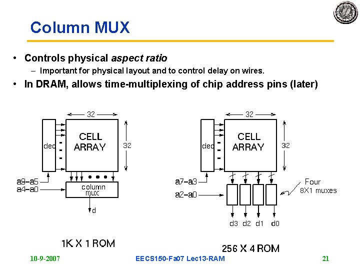
Column MUX • Controls physical aspect ratio – Important for physical layout and to control delay on wires. • In DRAM, allows time-multiplexing of chip address pins (later) 10 -9 -2007 EECS 150 -Fa 07 Lec 13 -RAM 21

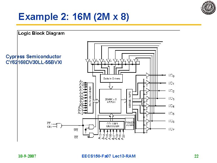
Example 2: 16 M (2 M x 8) Cypress Semiconductor CY 62168 DV 30 LL-55 BVXI 10 -9 -2007 EECS 150 -Fa 07 Lec 13 -RAM 22

Typical SRAM Timing A N WE_L OE determines direction Hi = Write, Lo = Read Writes are dangerous! Be careful! Double signaling: OE Hi, WE Lo 2 N words x M bit SRAM M D Write Timing: D Data In Read Timing: High Z Data Out Junk A Write Address Read Address OE_L Write Hold Time Read Access Time 10 -9 -2007 Write Setup Time EECS 150 -Fa 07 Lec 13 -RAM Read Access Time 23

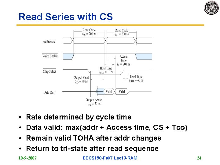
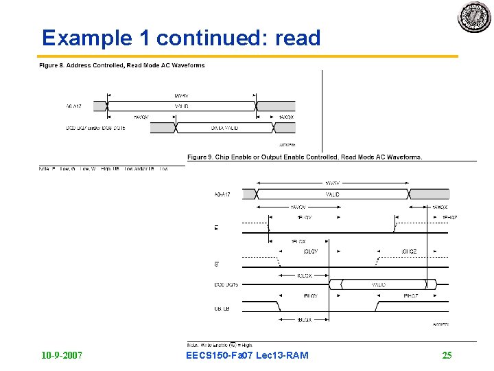
Read Series with CS • • Rate determined by cycle time Data valid: max(addr + Access time, CS + Tco) Remain valid TOHA after addr changes Return to tri-state after read sequence 10 -9 -2007 EECS 150 -Fa 07 Lec 13 -RAM 24

Example 1 continued: read 10 -9 -2007 EECS 150 -Fa 07 Lec 13 -RAM 25

Example 1 continued: write 10 -9 -2007 EECS 150 -Fa 07 Lec 13 -RAM 26

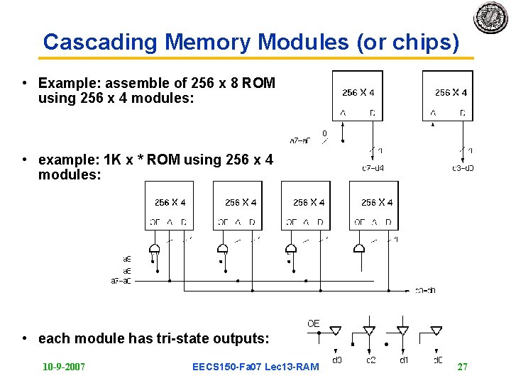
Cascading Memory Modules (or chips) • Example: assemble of 256 x 8 ROM using 256 x 4 modules: • example: 1 K x * ROM using 256 x 4 modules: • each module has tri-state outputs: 10 -9 -2007 EECS 150 -Fa 07 Lec 13 -RAM 27

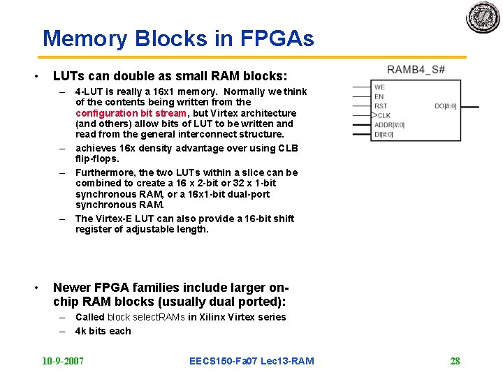
Memory Blocks in FPGAs • LUTs can double as small RAM blocks: – 4 -LUT is really a 16 x 1 memory. Normally we think of the contents being written from the configuration bit stream, but Virtex architecture (and others) allow bits of LUT to be written and read from the general interconnect structure. – achieves 16 x density advantage over using CLB flip-flops. – Furthermore, the two LUTs within a slice can be combined to create a 16 x 2 -bit or 32 x 1 -bit synchronous RAM, or a 16 x 1 -bit dual-port synchronous RAM. – The Virtex-E LUT can also provide a 16 -bit shift register of adjustable length. • Newer FPGA families include larger onchip RAM blocks (usually dual ported): – Called block select. RAMs in Xilinx Virtex series – 4 k bits each 10 -9 -2007 EECS 150 -Fa 07 Lec 13 -RAM 28

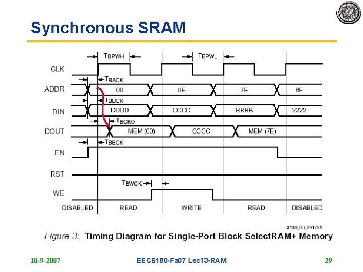
Synchronous SRAM 10 -9 -2007 EECS 150 -Fa 07 Lec 13 -RAM 29

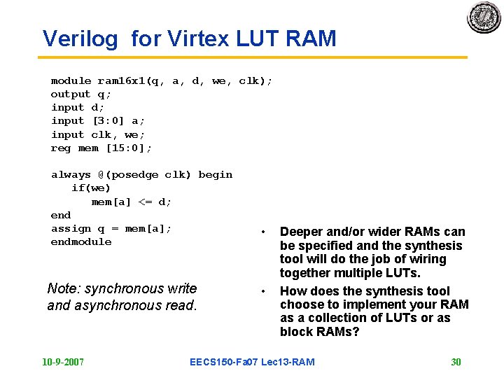
Verilog for Virtex LUT RAM module ram 16 x 1(q, a, d, we, clk); output q; input d; input [3: 0] a; input clk, we; reg mem [15: 0]; always @(posedge clk) begin if(we) mem[a] <= d; end assign q = mem[a]; endmodule Note: synchronous write and asynchronous read. 10 -9 -2007 • • Deeper and/or wider RAMs can be specified and the synthesis tool will do the job of wiring together multiple LUTs. How does the synthesis tool choose to implement your RAM as a collection of LUTs or as block RAMs? EECS 150 -Fa 07 Lec 13 -RAM 30

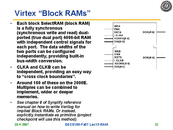
Virtex “Block RAMs” • • Each block Select. RAM (block RAM) is a fully synchronous (synchronous write and read) dualported (true dual port) 4096 -bit RAM with independent control signals for each port. The data widths of the two ports can be configured independently, providing built-in bus-width conversion. CLKA and CLKB can be independent, providing an easy way to “cross clock boundaries”. Around 160 of these on the 2000 E. Multiples can be combined to implement, wider or deeper memories. See chapter 8 of Synplify reference manual on how to write Verilog for implied Block RAMs. Or instead, explicitly instantiate as primitive (project checkpoint will use this method). 10 -9 -2007 EECS 150 -Fa 07 Lec 13 -RAM 31

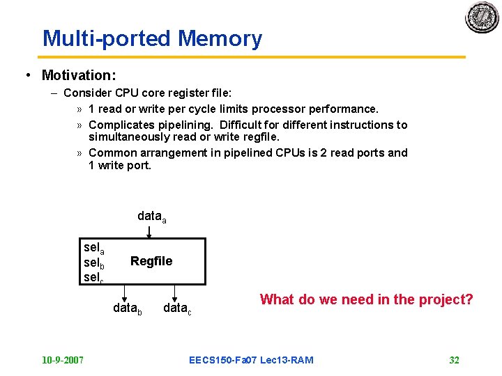
Multi-ported Memory • Motivation: – Consider CPU core register file: » 1 read or write per cycle limits processor performance. » Complicates pipelining. Difficult for different instructions to simultaneously read or write regfile. » Common arrangement in pipelined CPUs is 2 read ports and 1 write port. dataa selb selc Regfile datab 10 -9 -2007 datac What do we need in the project? EECS 150 -Fa 07 Lec 13 -RAM 32

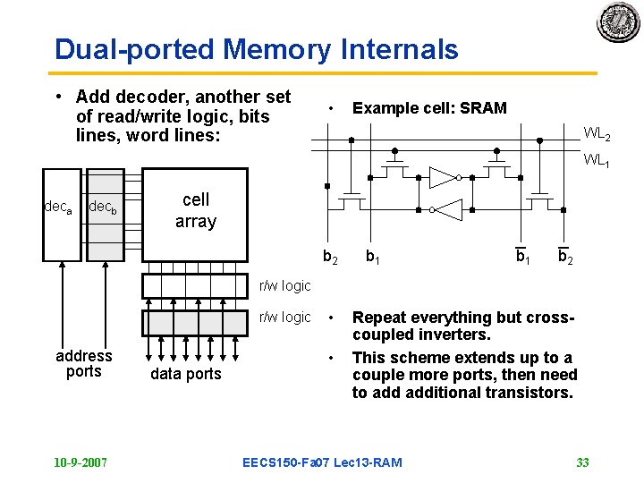
Dual-ported Memory Internals • Add decoder, another set of read/write logic, bits lines, word lines: • Example cell: SRAM WL 2 WL 1 deca decb cell array b 2 b 1 b 2 r/w logic address ports 10 -9 -2007 data ports • • Repeat everything but crosscoupled inverters. This scheme extends up to a couple more ports, then need to additional transistors. EECS 150 -Fa 07 Lec 13 -RAM 33

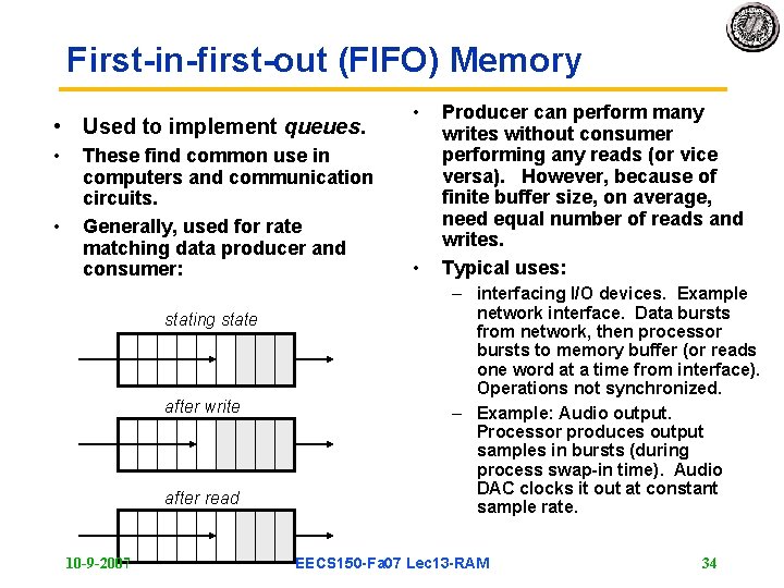
First-in-first-out (FIFO) Memory • Used to implement queues. • • These find common use in computers and communication circuits. Generally, used for rate matching data producer and consumer: stating state after write after read 10 -9 -2007 • • Producer can perform many writes without consumer performing any reads (or vice versa). However, because of finite buffer size, on average, need equal number of reads and writes. Typical uses: – interfacing I/O devices. Example network interface. Data bursts from network, then processor bursts to memory buffer (or reads one word at a time from interface). Operations not synchronized. – Example: Audio output. Processor produces output samples in bursts (during process swap-in time). Audio DAC clocks it out at constant sample rate. EECS 150 -Fa 07 Lec 13 -RAM 34

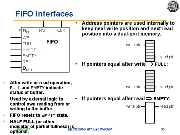
FIFO Interfaces DIN RST WE FULL HALF FULL EMPTY RE DOUT • • CLK FIFO • Address pointers are used internally to keep next write position and next read position into a dual-port memory. write ptr read ptr • If pointers equal after write FULL: After write or read operation, write ptr FULL and EMPTY indicate status of buffer. • If pointers equal after read Used by external logic to control own reading from or write ptr writing to the buffer. FIFO resets to EMPTY state. HALF FULL (or other indicator of partial fullness) is 10 -9 -2007 EECS 150 -Fa 07 Lec 13 -RAM optional. read ptr EMPTY: read ptr 35

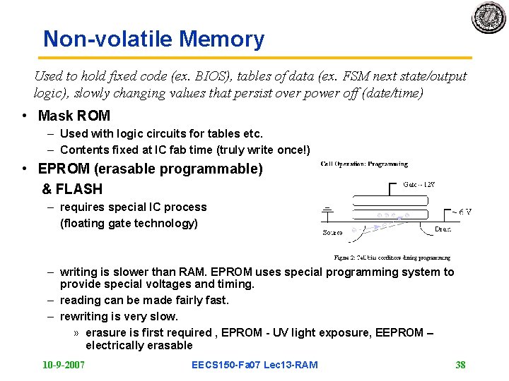
Non-volatile Memory Used to hold fixed code (ex. BIOS), tables of data (ex. FSM next state/output logic), slowly changing values that persist over power off (date/time) • Mask ROM – Used with logic circuits for tables etc. – Contents fixed at IC fab time (truly write once!) • EPROM (erasable programmable) & FLASH – requires special IC process (floating gate technology) – writing is slower than RAM. EPROM uses special programming system to provide special voltages and timing. – reading can be made fairly fast. – rewriting is very slow. » erasure is first required , EPROM - UV light exposure, EEPROM – electrically erasable 10 -9 -2007 EECS 150 -Fa 07 Lec 13 -RAM 38

FLASH Memory • Electrically erasable • In system programmability and erasability (no special system or voltages needed) • On-chip circuitry (FSM) and voltage generators to control erasure and programming (writing) • Erasure happens in variable sized "sectors" in a flash (16 K - 64 K Bytes) See: http: //developer. intel. com/design/flash/ for product descriptions, etc. • Compact flash cards are based on this type of memory. – NAND flash – Configuration memory, microcontrollers usually NOR flash 10 -9 -2007 EECS 150 -Fa 07 Lec 13 -RAM 39

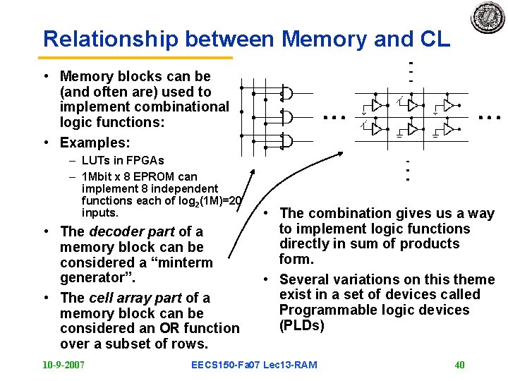
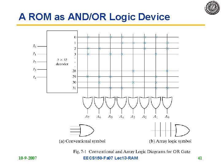
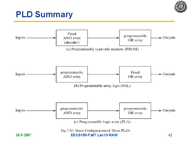
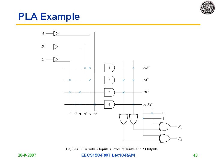
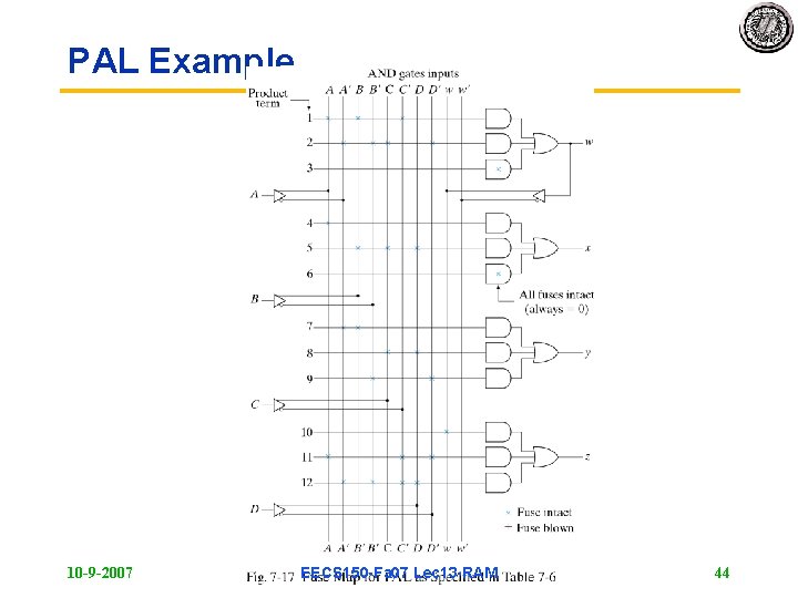
Relationship between Memory and CL • Memory blocks can be (and often are) used to implement combinational logic functions: • Examples: – LUTs in FPGAs – 1 Mbit x 8 EPROM can implement 8 independent functions each of log 2(1 M)=20 inputs. • The decoder part of a memory block can be considered a “minterm generator”. • The cell array part of a memory block can be considered an OR function over a subset of rows. 10 -9 -2007 • The combination gives us a way to implement logic functions directly in sum of products form. • Several variations on this theme exist in a set of devices called Programmable logic devices (PLDs) EECS 150 -Fa 07 Lec 13 -RAM 40

A ROM as AND/OR Logic Device 10 -9 -2007 EECS 150 -Fa 07 Lec 13 -RAM 41

PLD Summary 10 -9 -2007 EECS 150 -Fa 07 Lec 13 -RAM 42

PLA Example 10 -9 -2007 EECS 150 -Fa 07 Lec 13 -RAM 43

PAL Example 10 -9 -2007 EECS 150 -Fa 07 Lec 13 -RAM 44

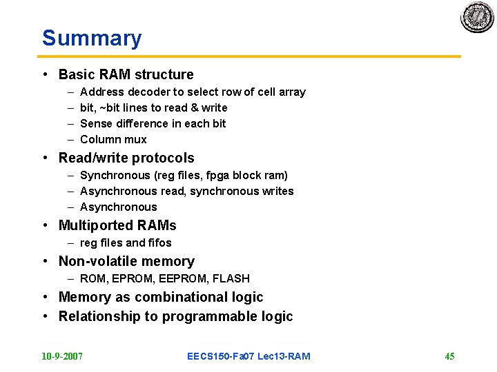
Summary • Basic RAM structure – – Address decoder to select row of cell array bit, ~bit lines to read & write Sense difference in each bit Column mux • Read/write protocols – Synchronous (reg files, fpga block ram) – Asynchronous read, synchronous writes – Asynchronous • Multiported RAMs – reg files and fifos • Non-volatile memory – ROM, EPROM, EEPROM, FLASH • Memory as combinational logic • Relationship to programmable logic 10 -9 -2007 EECS 150 -Fa 07 Lec 13 -RAM 45