CSE 140 Components and Design Techniques for Digital
- Slides: 50

CSE 140: Components and Design Techniques for Digital Systems Lecture 7: Sequential Networks CK Cheng Dept. of Computer Science and Engineering University of California, San Diego 1

What is a sequential circuit? “A circuit whose output depends on current inputs and past outputs” “A circuit with memory” Memory => Time 2

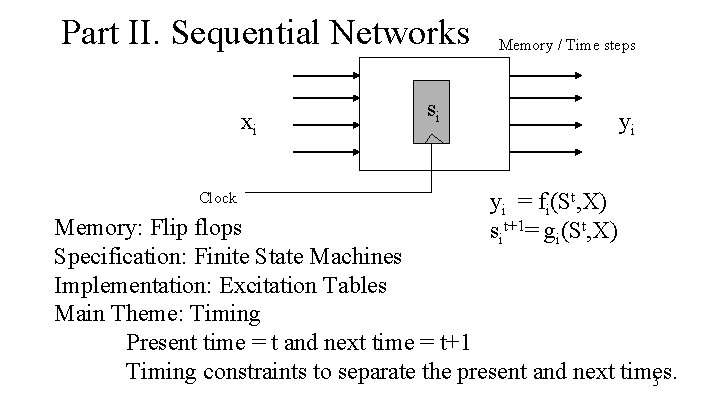
Part II. Sequential Networks xi Clock Memory / Time steps si yi yi = fi(St, X) sit+1= gi(St, X) Memory: Flip flops Specification: Finite State Machines Implementation: Excitation Tables Main Theme: Timing Present time = t and next time = t+1 Timing constraints to separate the present and next times. 3

Sequential Networks • Memory Components – Hierarchy of Memory – Basic Mechanism of Memory – Types of Flip-Flops • Implementation – Finite State Machine 4

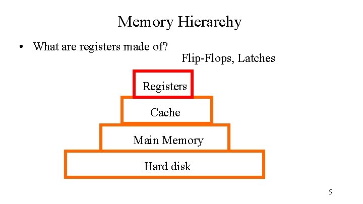
Memory Hierarchy • What are registers made of? Flip-Flops, Latches Registers Cache Main Memory Hard disk 5

The usage of a sequential machine i. Clicker Question: A. Digital systems are implemented using sequential machines. B. Only a small subset of digital systems can be implemented using sequential machines. C. Sequential machines are too simple for complicated digital systems. 6

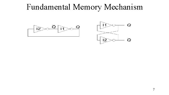
Fundamental Memory Mechanism 7

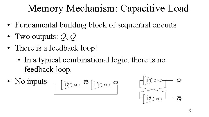
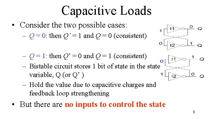
Memory Mechanism: Capacitive Load • Fundamental building block of sequential circuits • Two outputs: Q, Q • There is a feedback loop! • In a typical combinational logic, there is no feedback loop. • No inputs 8

Capacitive Loads • Consider the two possible cases: – Q = 0: then Q’ = 1 and Q = 0 (consistent) – Q = 1: then Q’ = 0 and Q = 1 (consistent) – Bistable circuit stores 1 bit of state in the state variable, Q (or Q’ ) – Hold the value due to capacitive charges and feedback loop strengthening • But there are no inputs to control the state 9

i. Clicker Q. Given a memory component made out of a loop of inverters, the number of inverters in the loop has to be A. Even B. Odd 10

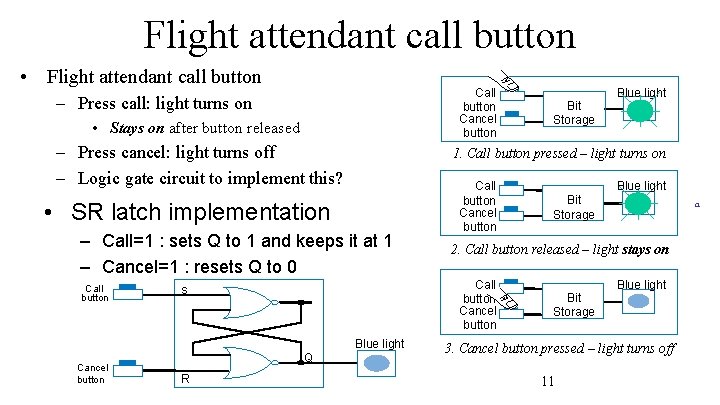
Flight attendant call button • Flight attendant call button Cancel button – Press call: light turns on • Stays on after button released – Press cancel: light turns off – Logic gate circuit to implement this? – Call=1 : sets Q to 1 and keeps it at 1 – Cancel=1 : resets Q to 0 Blue light Cancel button R Call button Cancel button Blue light Bit Storage a 2. Call button released – light stays on Call button Cancel button S Q Blue light 1. Call button pressed – light turns on • SR latch implementation Call button Bit Storage Blue light 3. Cancel button pressed – light turns off 11

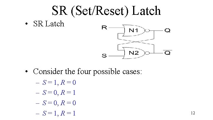
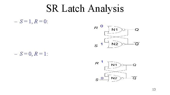
SR (Set/Reset) Latch • SR Latch • Consider the four possible cases: – – S = 1, R = 0 S = 0, R = 1 S = 0, R = 0 S = 1, R = 1 12

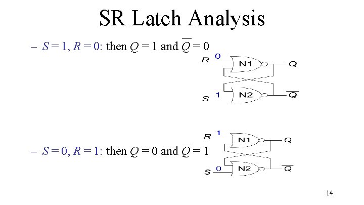
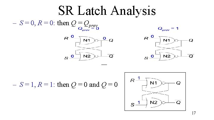
SR Latch Analysis – S = 1, R = 0: – S = 0, R = 1: 13

SR Latch Analysis – S = 1, R = 0: then Q = 1 and Q = 0 – S = 0, R = 1: then Q = 0 and Q = 1 14

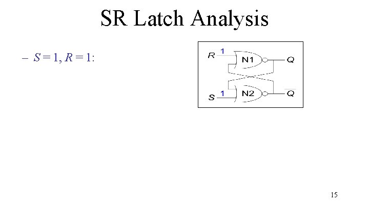
SR Latch Analysis – S = 1, R = 1: 15

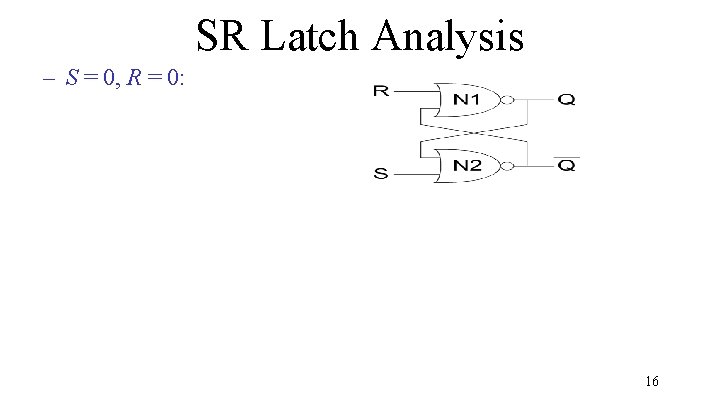
SR Latch Analysis – S = 0, R = 0: 16

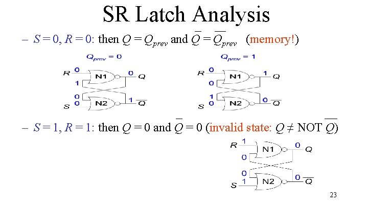
SR Latch Analysis – S = 0, R = 0: then Q = Qprev – S = 1, R = 1: then Q = 0 and Q = 0 17

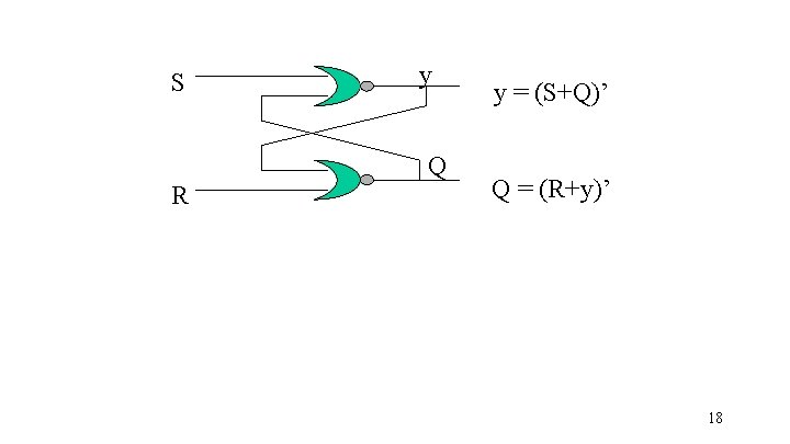
S y Q R y = (S+Q)’ Q = (R+y)’ 18

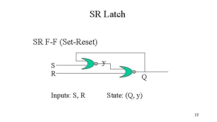
SR Latch SR F-F (Set-Reset) S R Inputs: S, R y Q State: (Q, y) 19

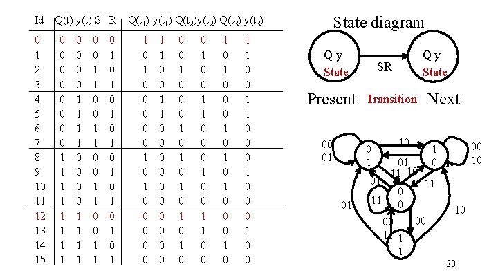
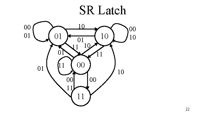
Id 0 1 2 3 4 5 6 7 8 9 10 11 12 13 14 15 State diagram Q(t) y(t) S R Q(t 1) y(t 1) Q(t 2)y(t 2) Q(t 3) y(t 3) 0 0 0 0 1 1 1 1 0 0 1 1 0 1 0 1 1 0 1 0 0 0 0 0 1 1 0 0 0 0 1 0 0 0 1 0 1 0 1 0 0 1 1 0 0 1 0 1 0 1 0 0 0 1 1 0 0 0 1 0 0 Qy State Present 00 01 SR Next Transition 0 1 01 01 Qy State 11 10 01 11 10 0 0 00 11 1 1 00 10 1 0 11 00 10 20

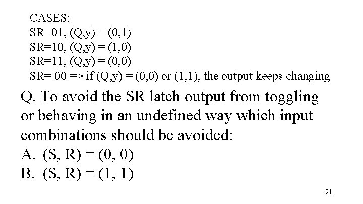
CASES: SR=01, (Q, y) = (0, 1) SR=10, (Q, y) = (1, 0) SR=11, (Q, y) = (0, 0) SR= 00 => if (Q, y) = (0, 0) or (1, 1), the output keeps changing Q. To avoid the SR latch output from toggling or behaving in an undefined way which input combinations should be avoided: A. (S, R) = (0, 0) B. (S, R) = (1, 1) 21

SR Latch 10 00 01 01 01 11 10 10 11 00 10 10 00 00 11 11 22

SR Latch Analysis – S = 0, R = 0: then Q = Qprev and Q = Qprev (memory!) – S = 1, R = 1: then Q = 0 and Q = 0 (invalid state: Q ≠ NOT Q) 23

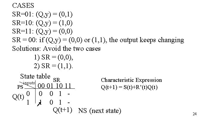
CASES SR=01: (Q, y) = (0, 1) SR=10: (Q, y) = (1, 0) SR=11: (Q, y) = (0, 0) SR = 00: if (Q, y) = (0, 0) or (1, 1), the output keeps changing Solutions: Avoid the two cases 1) SR = (0, 0), 2) SR = (1, 1). State table SR Characteristic Expression inputs 00 01 10 11 PS Q(t+1) = S(t)+R’(t)Q(t) 0 0 0 1 1 1 0 1 Q(t+1) NS (next state) 24

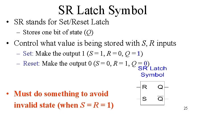
SR Latch Symbol • SR stands for Set/Reset Latch – Stores one bit of state (Q) • Control what value is being stored with S, R inputs – Set: Make the output 1 (S = 1, R = 0, Q = 1) – Reset: Make the output 0 (S = 0, R = 1, Q = 0) • Must do something to avoid invalid state (when S = R = 1) 25

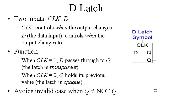
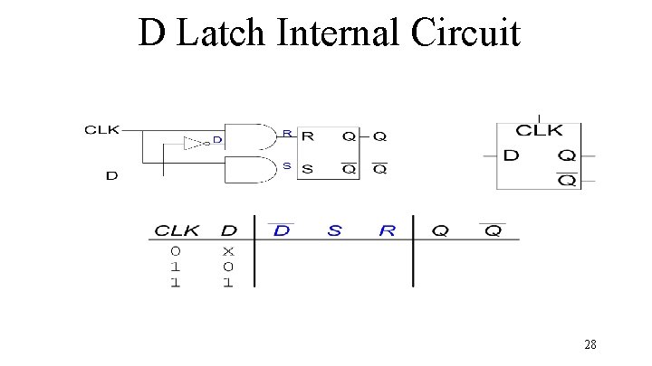
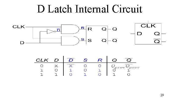
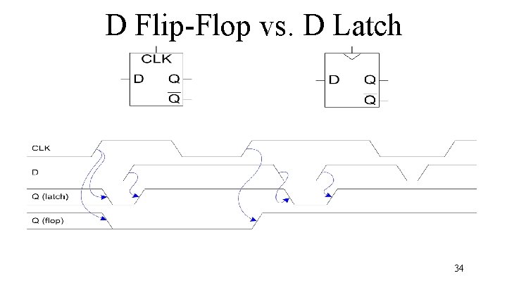
D Latch • Two inputs: CLK, D – CLK: controls when the output changes – D (the data input): controls what the output changes to • Function – When CLK = 1, D passes through to Q (the latch is transparent) – When CLK = 0, Q holds its previous value (the latch is opaque) • Avoids invalid case when Q ≠ NOT Q 26

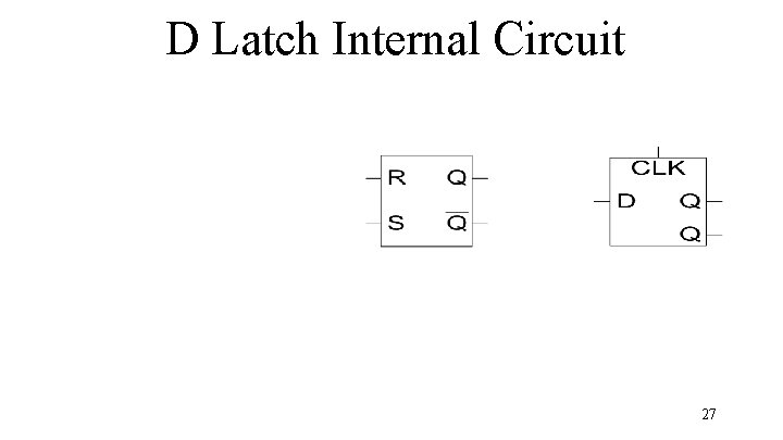
D Latch Internal Circuit 27

D Latch Internal Circuit 28

D Latch Internal Circuit 29

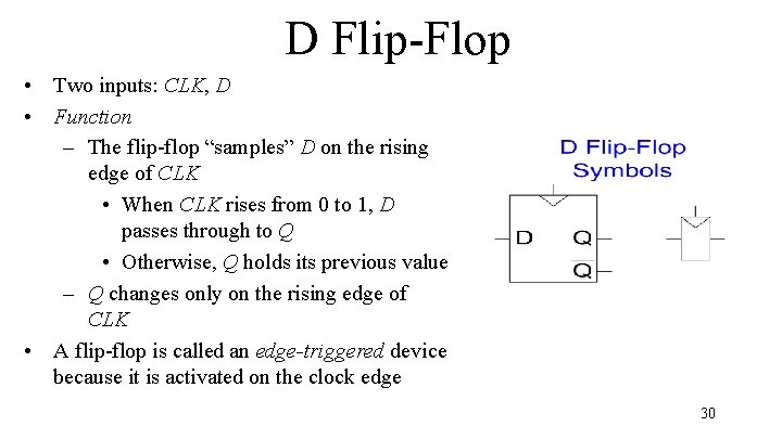
D Flip-Flop • Two inputs: CLK, D • Function – The flip-flop “samples” D on the rising edge of CLK • When CLK rises from 0 to 1, D passes through to Q • Otherwise, Q holds its previous value – Q changes only on the rising edge of CLK • A flip-flop is called an edge-triggered device because it is activated on the clock edge 30

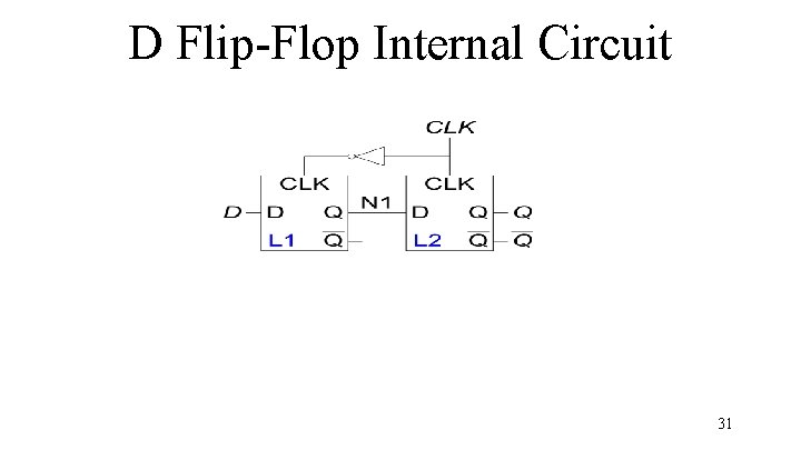
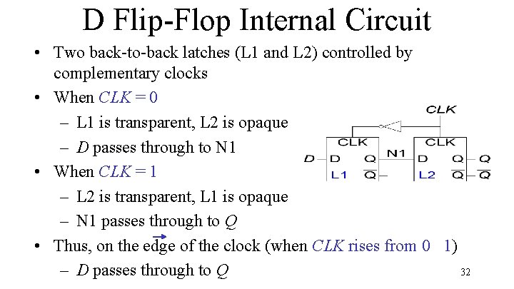
D Flip-Flop Internal Circuit 31

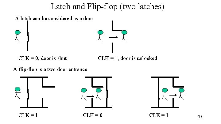
D Flip-Flop Internal Circuit • Two back-to-back latches (L 1 and L 2) controlled by complementary clocks • When CLK = 0 – L 1 is transparent, L 2 is opaque – D passes through to N 1 • When CLK = 1 – L 2 is transparent, L 1 is opaque – N 1 passes through to Q • Thus, on the edge of the clock (when CLK rises from 0 1) 32 – D passes through to Q

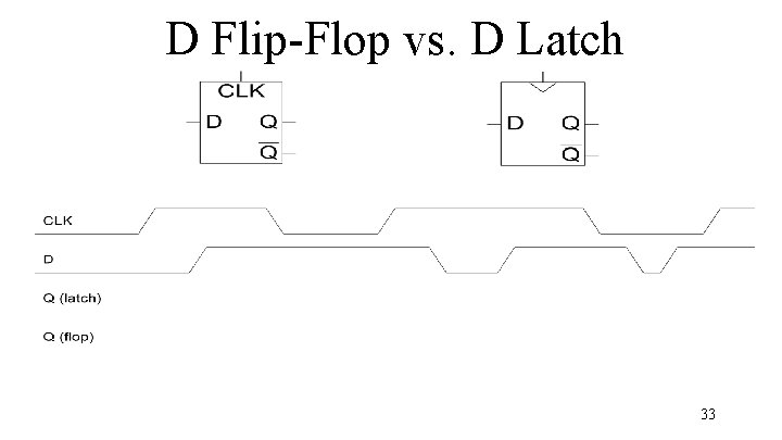
D Flip-Flop vs. D Latch 33

D Flip-Flop vs. D Latch 34

Latch and Flip-flop (two latches) A latch can be considered as a door CLK = 0, door is shut CLK = 1, door is unlocked A flip-flop is a two door entrance CLK = 1 CLK = 0 CLK = 1 35

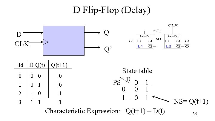
D Flip-Flop (Delay) Q D CLK Q’ Id D Q(t) Q(t+1) 0 0 1 2 3 0 1 1 State table PS D 0 1 0 1 Characteristic Expression: Q(t+1) = D(t) NS= Q(t+1) 36

i. Clicker Can D flip-flip serve as a memory component? A. Yes B. No 37

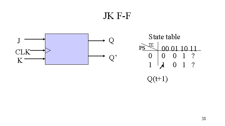
JK F-F J Q CLK K Q’ State table PS JK 0 1 00 01 10 11 0 0 1 ? 1 0 1 ? Q(t+1) 38

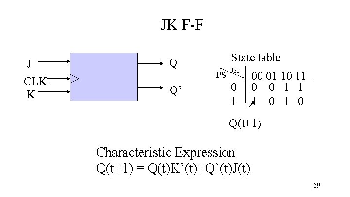
JK F-F J Q CLK K Q’ State table PS JK 0 1 00 01 10 11 0 0 1 1 1 0 Q(t+1) Characteristic Expression Q(t+1) = Q(t)K’(t)+Q’(t)J(t) 39

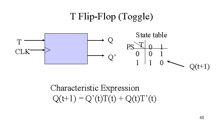
T Flip-Flop (Toggle) T CLK Q Q’ State table PS T 0 1 0 0 1 1 1 0 Q(t+1) Characteristic Expression Q(t+1) = Q’(t)T(t) + Q(t)T’(t) 40

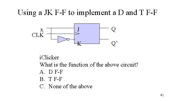
Using a JK F-F to implement a D and T F-F x CLK J Q K Q’ i. Clicker What is the function of the above circuit? A. D F-F B. T F-F C. None of the above 41

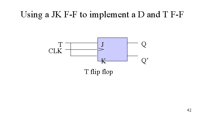
Using a JK F-F to implement a D and T F-F T CLK J Q K Q’ T flip flop 42

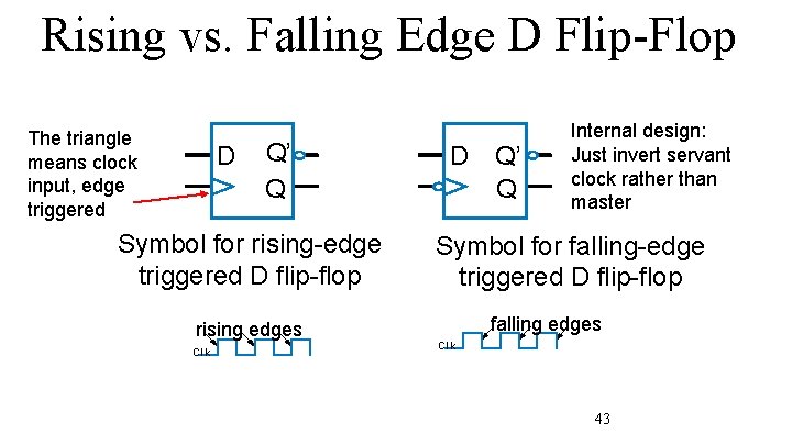
Rising vs. Falling Edge D Flip-Flop The triangle means clock input, edge triggered D Q’ Q Symbol for rising-edge triggered D flip-flop rising edges Clk D Q’ Q Internal design: Just invert servant clock rather than master Symbol for falling-edge triggered D flip-flop falling edges Clk 43

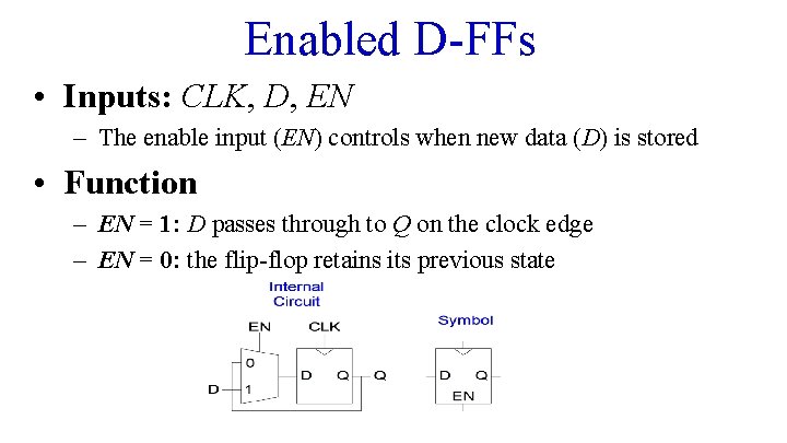
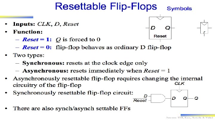
Enabled D-FFs • Inputs: CLK, D, EN – The enable input (EN) controls when new data (D) is stored • Function – EN = 1: D passes through to Q on the clock edge – EN = 0: the flip-flop retains its previous state

45

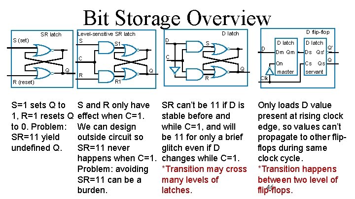
Bit Storage Overview S (set) D R (reset) S=1 sets Q to 1, R=1 resets Q to 0. Problem: SR=11 yield undefined Q. R S D C C Q D flip-flop D latch Level-sensitive SR latch S S 1 SR latch Q Q R 1 S and R only have effect when C=1. We can design outside circuit so SR=11 never happens when C=1. Problem: avoiding SR=11 can be a burden. R SR can’t be 11 if D is stable before and while C=1, and will be 11 for only a brief glitch even if D changes while C=1. *Transition may cross many levels of latches. D latch Dm Qm Ds Qs’ Cm master Cs Qs servant Q’ Q Clk Only loads D value present at rising clock edge, so values can’t propagate to other flipflops during same clock cycle. *Transition happens between two level of 46 flip-flops.

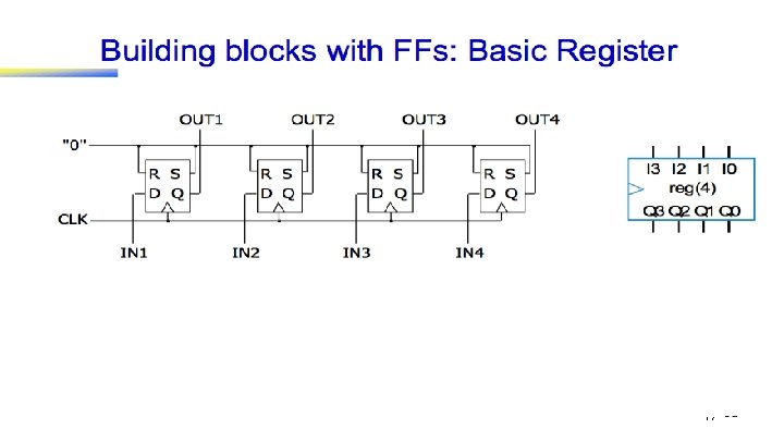
47

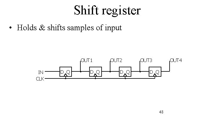
Shift register • Holds & shifts samples of input OUT 1 IN CLK D Q OUT 2 D Q OUT 3 OUT 4 D Q 48

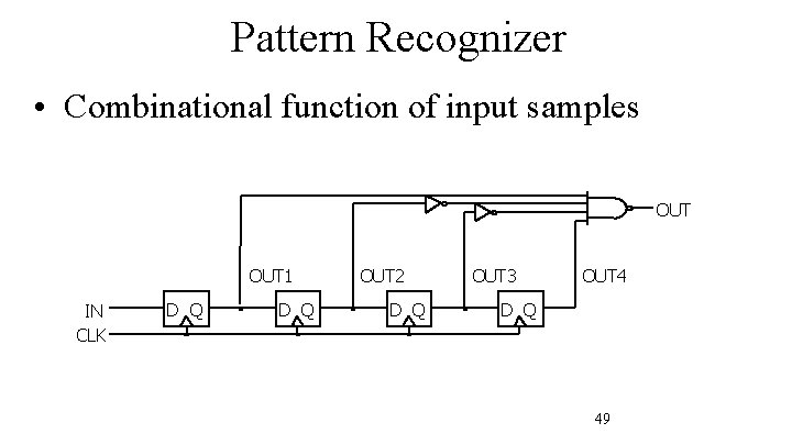
Pattern Recognizer • Combinational function of input samples OUT 1 IN CLK D Q OUT 2 D Q OUT 3 OUT 4 D Q 49

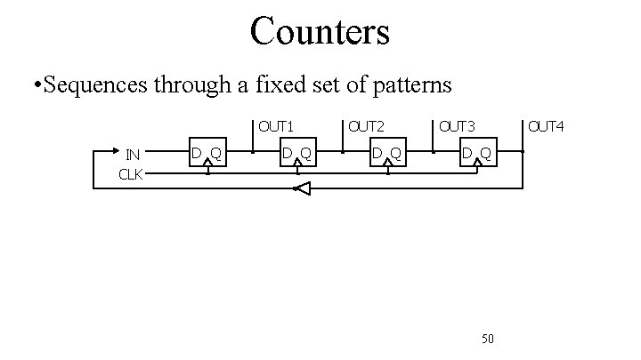
Counters • Sequences through a fixed set of patterns OUT 1 IN CLK D Q OUT 2 D Q OUT 3 OUT 4 D Q 50