CSE 140 Lecture 14 System Designs CK Cheng
![Implementation: Example Add. Module(X, Y, Z, start, done) { Input X[15: 0], Y[15: 0] Implementation: Example Add. Module(X, Y, Z, start, done) { Input X[15: 0], Y[15: 0]](https://slidetodoc.com/presentation_image/ade4382411fe236ec7bd7ecba74767c7/image-18.jpg)
- Slides: 18

CSE 140 Lecture 14 System Designs CK Cheng CSE Dept. UC San Diego 1

System Designs • Introduction • Components • Spec • Implementation 2

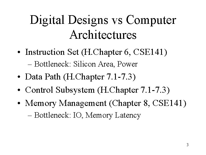
Digital Designs vs Computer Architectures • Instruction Set (H. Chapter 6, CSE 141) – Bottleneck: Silicon Area, Power • Data Path (H. Chapter 7. 1 -7. 3) • Control Subsystem (H. Chapter 7. 1 -7. 3) • Memory Management (Chapter 8, CSE 141) – Bottleneck: IO, Memory Latency 3

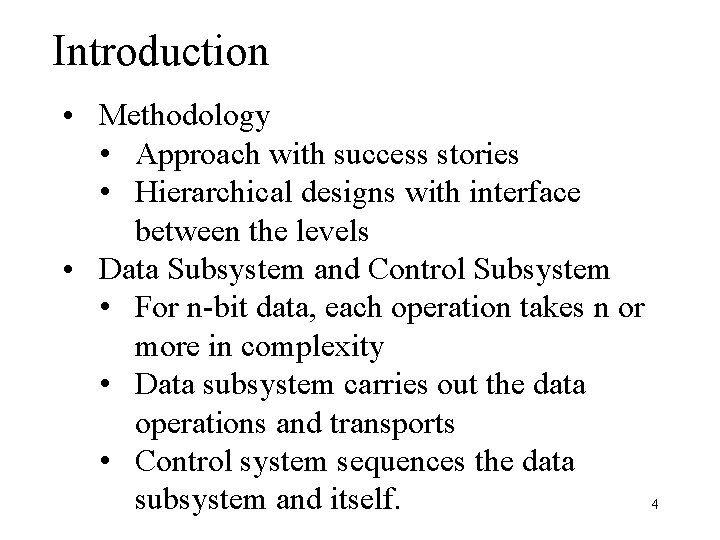
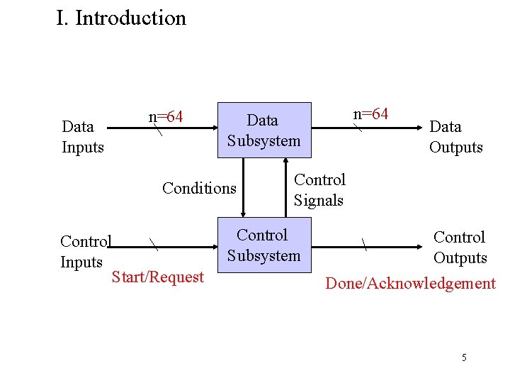
Introduction • Methodology • Approach with success stories • Hierarchical designs with interface between the levels • Data Subsystem and Control Subsystem • For n-bit data, each operation takes n or more in complexity • Data subsystem carries out the data operations and transports • Control system sequences the data 4 subsystem and itself.

I. Introduction Data Inputs n=64 Conditions Control Inputs Start/Request n=64 Data Subsystem Data Outputs Control Signals Control Subsystem Control Outputs Done/Acknowledgement 5

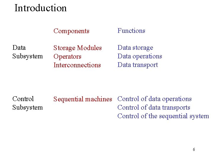
Introduction Components Functions Data Subsystem Storage Modules Operators Interconnections Data storage Data operations Data transport Control Subsystem Sequential machines Control of data operations Control of data transports Control of the sequential system 6

Data Subsystem Components • Storage • Operator • Interconnect 7

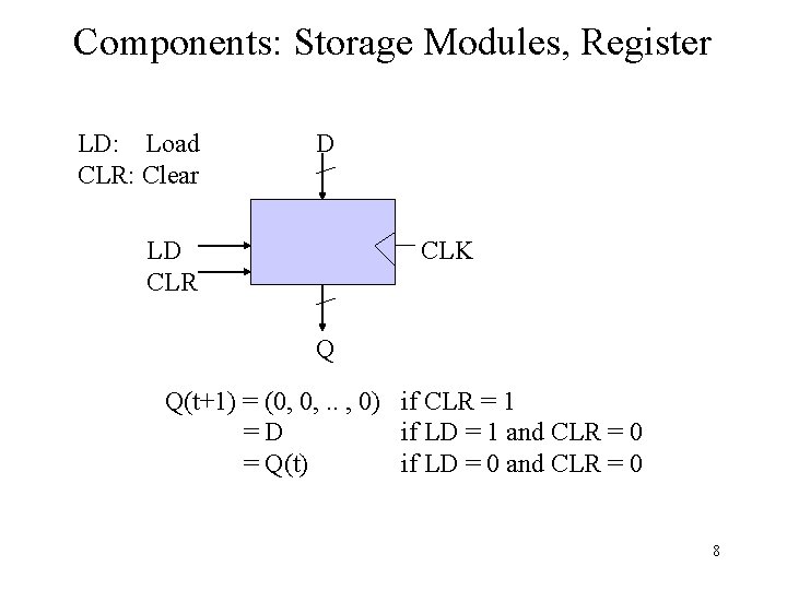
Components: Storage Modules, Register LD: Load CLR: Clear D CLK LD CLR Q Q(t+1) = (0, 0, . . , 0) if CLR = 1 =D if LD = 1 and CLR = 0 = Q(t) if LD = 0 and CLR = 0 8

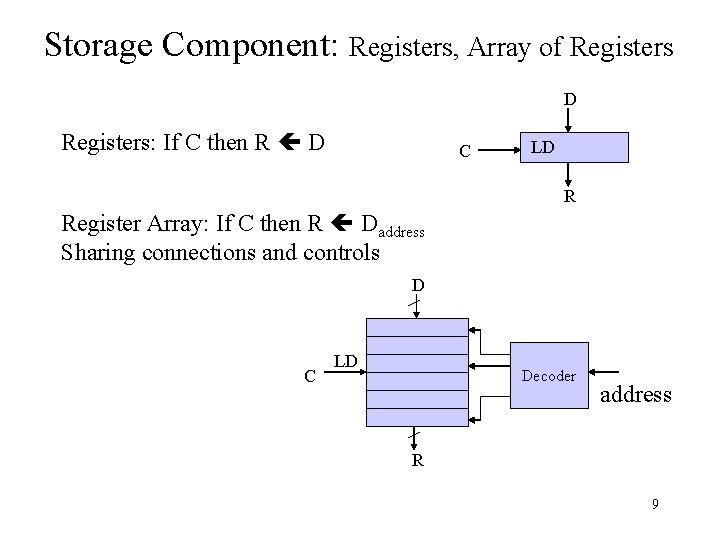
Storage Component: Registers, Array of Registers D Registers: If C then R D C LD R Register Array: If C then R Daddress Sharing connections and controls D C LD Decoder address R 9

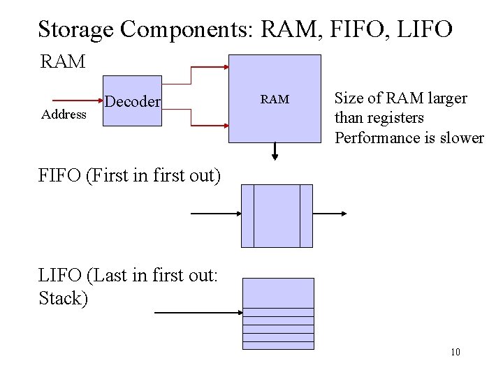
Storage Components: RAM, FIFO, LIFO RAM Address Decoder RAM Size of RAM larger than registers Performance is slower FIFO (First in first out) LIFO (Last in first out: Stack) 10

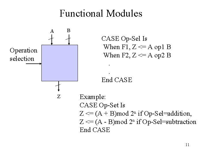
Functional Modules B A CASE Op-Sel Is When F 1, Z <= A op 1 B When F 2, Z <= A op 2 B. . End CASE Operation selection Z Example: CASE Op-Set Is Z <= (A + B)mod 2 n if Op-Sel=addition, Z <= (A - B)mod 2 n if Op-Sel=subtraction End CASE 11

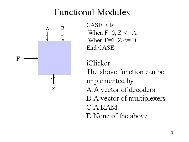
Functional Modules B A F Z CASE F Is When F=0, Z <= A When F=1, Z <= B End CASE i. Clicker: The above function can be implemented by A. A vector of decoders B. A vector of multiplexers C. A RAM D. None of the above 12

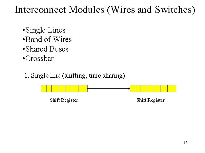
Interconnect Modules (Wires and Switches) • Single Lines • Band of Wires • Shared Buses • Crossbar 1. Single line (shifting, time sharing) Shift Register 13

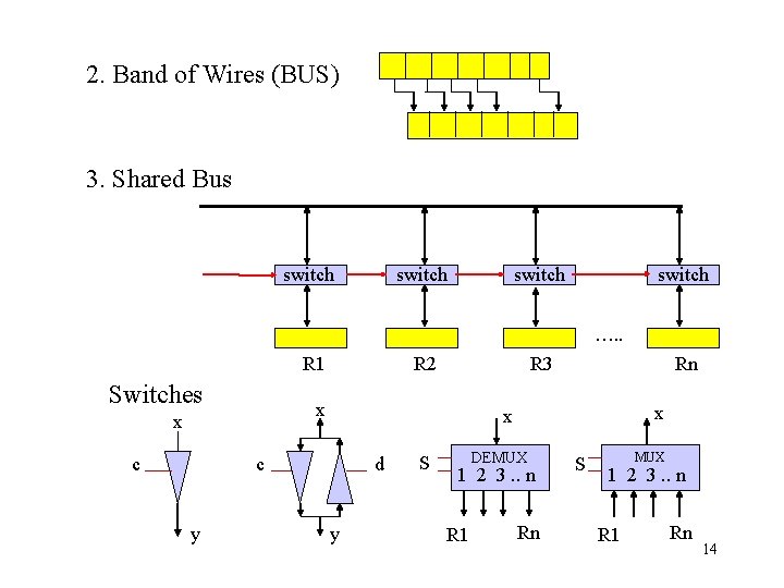
2. Band of Wires (BUS) 3. Shared Bus switch …. . R 1 Switches Rn x x c y R 3 x x c R 2 d y S DEMUX 1 2 3. . n R 1 Rn S MUX 1 2 3. . n R 1 Rn 14

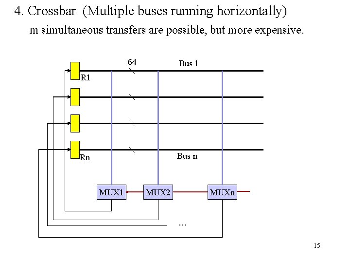
4. Crossbar (Multiple buses running horizontally) m simultaneous transfers are possible, but more expensive. 64 Bus 1 R 1 Bus n Rn MUX 1 MUX 2 MUXn … 15

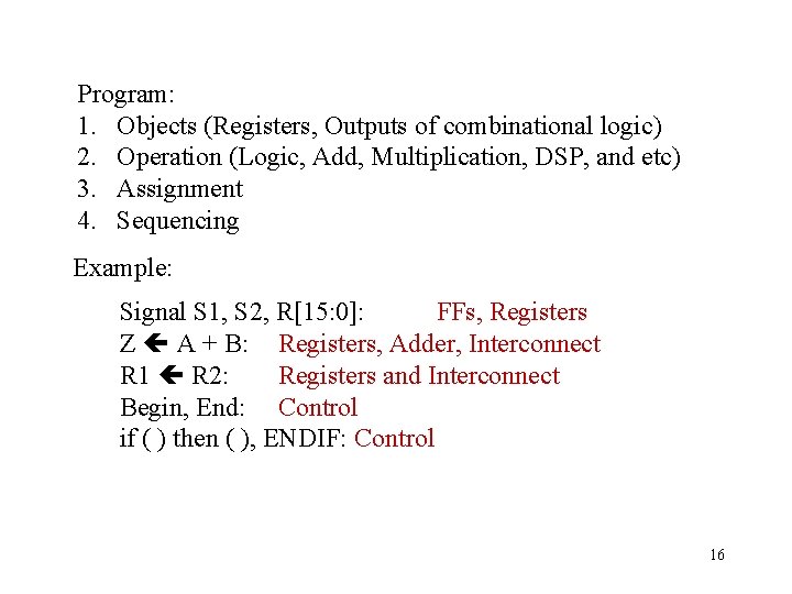
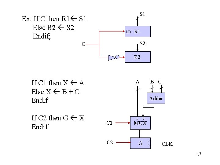
Program: 1. Objects (Registers, Outputs of combinational logic) 2. Operation (Logic, Add, Multiplication, DSP, and etc) 3. Assignment 4. Sequencing Example: Signal S 1, S 2, R[15: 0]: FFs, Registers Z A + B: Registers, Adder, Interconnect R 1 R 2: Registers and Interconnect Begin, End: Control if ( ) then ( ), ENDIF: Control 16

S 1 Ex. If C then R 1 S 1 Else R 2 S 2 Endif; LD R 1 S 2 C R 2 A If C 1 then X A Else X B + C Endif If C 2 then G X Endif B C Adder 1 0 C 1 MUX C 2 G CLK 17
![Implementation Example Add ModuleX Y Z start done Input X15 0 Y15 0 Implementation: Example Add. Module(X, Y, Z, start, done) { Input X[15: 0], Y[15: 0]](https://slidetodoc.com/presentation_image/ade4382411fe236ec7bd7ecba74767c7/image-18.jpg)
Implementation: Example Add. Module(X, Y, Z, start, done) { Input X[15: 0], Y[15: 0] type bit-vector, start type boolean; Local-Object A[15: 0], B[15: 0] type bit-vector; Output Z[15: 0] type bit-vector, done type boolean; S 0: If start’ goto S 0 || done 1; S 1: A X || B Y || done 0; S 2: Z Add(A, B) || goto S 0; } Exercise: Go through the handshaking, data subsystem and control subsystem designs. 18