Understanding and Overcoming Challenges of DRAM Refresh Onur

![An Example: RAIDR [Liu+, ISCA 2012] 1. Profiling: Profile the retention time of all An Example: RAIDR [Liu+, ISCA 2012] 1. Profiling: Profile the retention time of all](https://slidetodoc.com/presentation_image_h/3461c0226393c6d3c758b306433c3321/image-28.jpg)
![Our Goal [Liu+, ISCA 2013] n Analyze the retention time behavior of DRAM cells Our Goal [Liu+, ISCA 2013] n Analyze the retention time behavior of DRAM cells](https://slidetodoc.com/presentation_image_h/3461c0226393c6d3c758b306433c3321/image-38.jpg)



![Summary and Conclusions [ISCA’ 13] n n DRAM refresh is a critical challenge in Summary and Conclusions [ISCA’ 13] n n DRAM refresh is a critical challenge in](https://slidetodoc.com/presentation_image_h/3461c0226393c6d3c758b306433c3321/image-86.jpg)
![Comparison Points • All-bank refresh [DDR 3, LPDDR 3, …] • Per-bank refresh [LPDDR Comparison Points • All-bank refresh [DDR 3, LPDDR 3, …] • Per-bank refresh [LPDDR](https://slidetodoc.com/presentation_image_h/3461c0226393c6d3c758b306433c3321/image-95.jpg)
- Slides: 99

Understanding and Overcoming Challenges of DRAM Refresh Onur Mutlu onur@cmu. edu June 30, 2014 Extreme Scale Scientific Computing Workshop

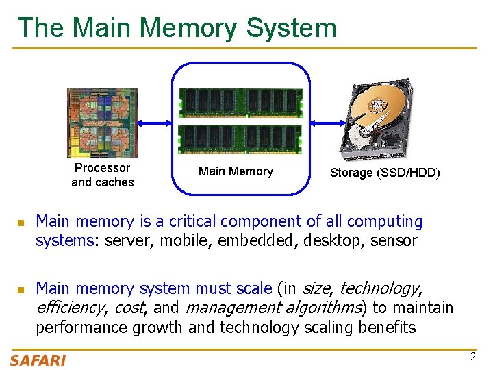
The Main Memory System Processor and caches n n Main Memory Storage (SSD/HDD) Main memory is a critical component of all computing systems: server, mobile, embedded, desktop, sensor Main memory system must scale (in size, technology, efficiency, cost, and management algorithms) to maintain performance growth and technology scaling benefits 2

State of the Main Memory System n Recent technology, architecture, and application trends q q n n n lead to new requirements exacerbate old requirements DRAM and memory controllers, as we know them today, are (will be) unlikely to satisfy all requirements Some emerging non-volatile memory technologies (e. g. , PCM) enable new opportunities: memory+storage merging We need to rethink the main memory system q q to fix DRAM issues and enable emerging technologies to satisfy all requirements 3

Agenda n n n Major Trends Affecting Main Memory The DRAM Scaling Problem Refresh as a Limiter of DRAM Scaling Solution Directions and Challenges Summary 4

Major Trends Affecting Main Memory (I) n Need for main memory capacity, bandwidth, Qo. S increasing n Main memory energy/power is a key system design concern n DRAM technology scaling is ending 5

Major Trends Affecting Main Memory (II) n Need for main memory capacity, bandwidth, Qo. S increasing q q q Multi-core: increasing number of cores/agents Data-intensive applications: increasing demand/hunger for data Consolidation: cloud computing, GPUs, mobile, heterogeneity n Main memory energy/power is a key system design concern n DRAM technology scaling is ending 6

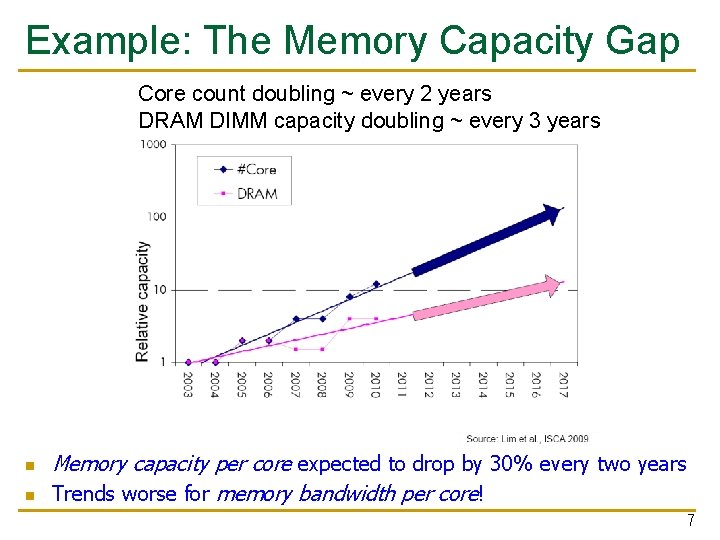
Example: The Memory Capacity Gap Core count doubling ~ every 2 years DRAM DIMM capacity doubling ~ every 3 years n n Memory capacity per core expected to drop by 30% every two years Trends worse for memory bandwidth per core! 7

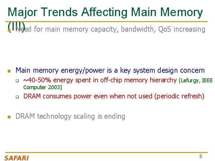
Major Trends Affecting Main Memory (III) n Need for main memory capacity, bandwidth, Qo. S increasing n Main memory energy/power is a key system design concern q ~40 -50% energy spent in off-chip memory hierarchy [Lefurgy, IEEE Computer 2003] q n DRAM consumes power even when not used (periodic refresh) DRAM technology scaling is ending 8

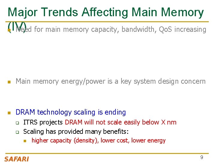
Major Trends Affecting Main Memory (IV) n Need for main memory capacity, bandwidth, Qo. S increasing n Main memory energy/power is a key system design concern n DRAM technology scaling is ending q q ITRS projects DRAM will not scale easily below X nm Scaling has provided many benefits: n higher capacity (density), lower cost, lower energy 9

Agenda n n n Major Trends Affecting Main Memory The DRAM Scaling Problem Refresh as a Limiter of DRAM Scaling Challenges and Solution Directions Summary 10

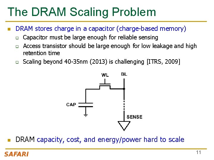
The DRAM Scaling Problem n DRAM stores charge in a capacitor (charge-based memory) q q q n Capacitor must be large enough for reliable sensing Access transistor should be large enough for low leakage and high retention time Scaling beyond 40 -35 nm (2013) is challenging [ITRS, 2009] DRAM capacity, cost, and energy/power hard to scale 11

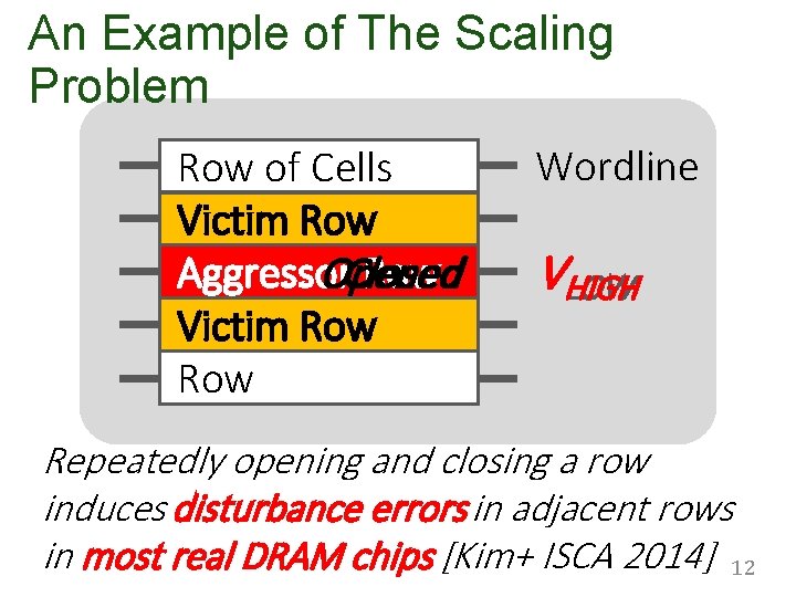
An Example of The Scaling Problem Row of Cells Row Victim Row Opened Aggressor Row Closed Row Victim Row Wordline VHIGH LOW Repeatedly opening and closing a row induces disturbance errors in adjacent rows in most real DRAM chips [Kim+ ISCA 2014] 12

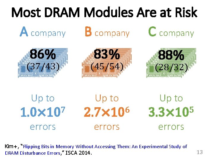
Most DRAM Modules Are at Risk A company B company C company 86% 83% (37/43) (45/54) (28/32) Up to 7 1. 0× 10 6 2. 7× 10 5 3. 3× 10 errors 88% Kim+, “Flipping Bits in Memory Without Accessing Them: An Experimental Study of DRAM Disturbance Errors, ” ISCA 2014. 13

Agenda n n n Major Trends Affecting Main Memory The DRAM Scaling Problem Refresh as a Limiter of DRAM Scaling Some Solution Directions and Challenges Summary 14

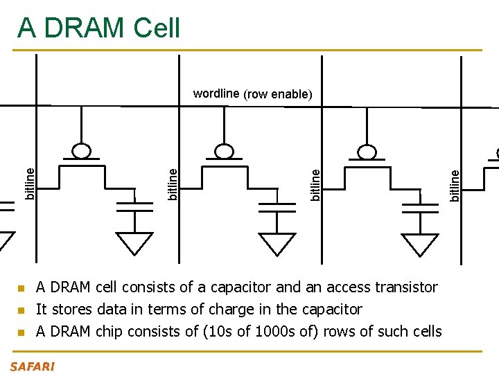
A DRAM Cell n n n A DRAM cell consists of a capacitor and an access transistor It stores data in terms of charge in the capacitor A DRAM chip consists of (10 s of 1000 s of) rows of such cells bitline wordline (row enable)

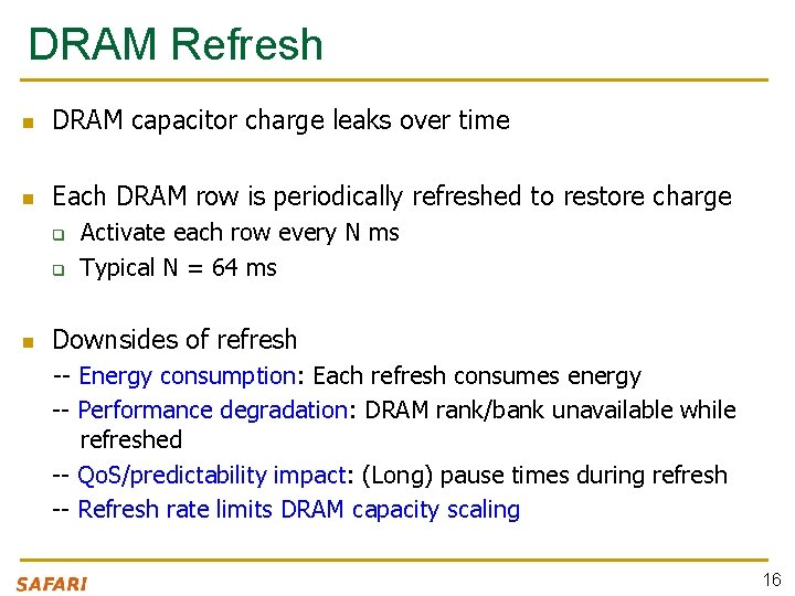
DRAM Refresh n DRAM capacitor charge leaks over time n Each DRAM row is periodically refreshed to restore charge q q n Activate each row every N ms Typical N = 64 ms Downsides of refresh -- Energy consumption: Each refresh consumes energy -- Performance degradation: DRAM rank/bank unavailable while refreshed -- Qo. S/predictability impact: (Long) pause times during refresh -- Refresh rate limits DRAM capacity scaling 16

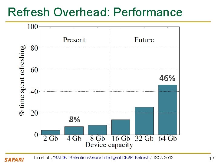
Refresh Overhead: Performance 46% 8% Liu et al. , “RAIDR: Retention-Aware Intelligent DRAM Refresh, ” ISCA 2012. 17

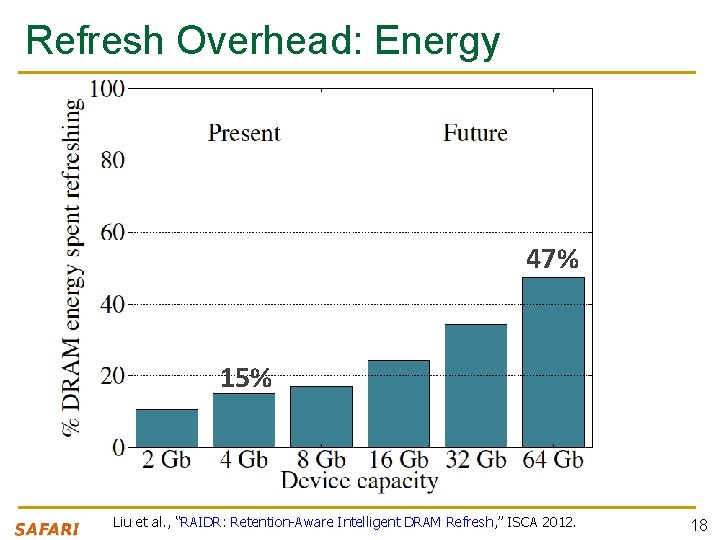
Refresh Overhead: Energy 47% 15% Liu et al. , “RAIDR: Retention-Aware Intelligent DRAM Refresh, ” ISCA 2012. 18

Agenda n n n Major Trends Affecting Main Memory The DRAM Scaling Problem Refresh as a Limiter of DRAM Scaling Some Solution Directions and Challenges Summary 19

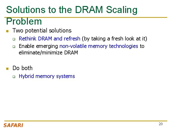
Solutions to the DRAM Scaling Problem n Two potential solutions q q n Rethink DRAM and refresh (by taking a fresh look at it) Enable emerging non-volatile memory technologies to eliminate/minimize DRAM Do both q Hybrid memory systems 20

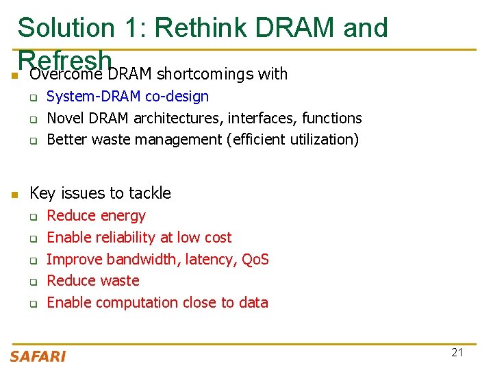
Solution 1: Rethink DRAM and Refresh n Overcome DRAM shortcomings with q q q n System-DRAM co-design Novel DRAM architectures, interfaces, functions Better waste management (efficient utilization) Key issues to tackle q q q Reduce energy Enable reliability at low cost Improve bandwidth, latency, Qo. S Reduce waste Enable computation close to data 21

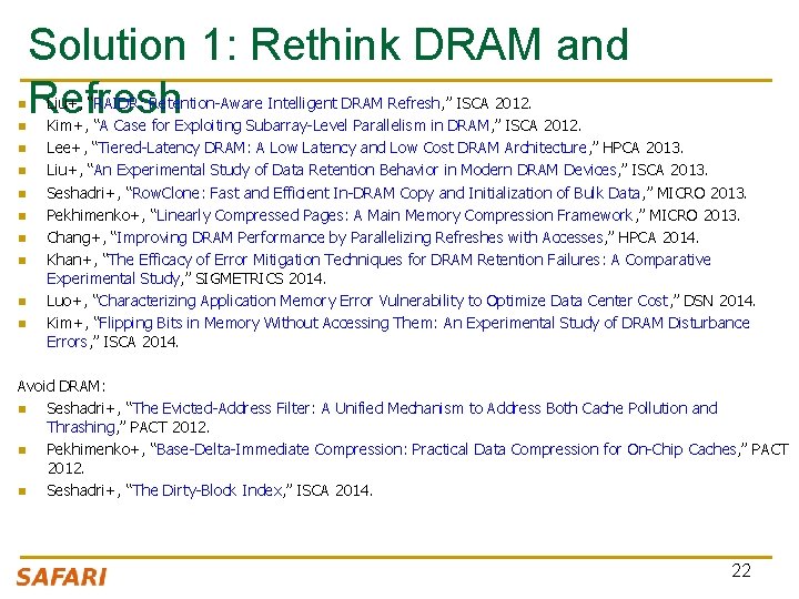
n n n n n Solution 1: Rethink DRAM and Refresh Liu+, “RAIDR: Retention-Aware Intelligent DRAM Refresh, ” ISCA 2012. Kim+, “A Case for Exploiting Subarray-Level Parallelism in DRAM, ” ISCA 2012. Lee+, “Tiered-Latency DRAM: A Low Latency and Low Cost DRAM Architecture, ” HPCA 2013. Liu+, “An Experimental Study of Data Retention Behavior in Modern DRAM Devices, ” ISCA 2013. Seshadri+, “Row. Clone: Fast and Efficient In-DRAM Copy and Initialization of Bulk Data, ” MICRO 2013. Pekhimenko+, “Linearly Compressed Pages: A Main Memory Compression Framework, ” MICRO 2013. Chang+, “Improving DRAM Performance by Parallelizing Refreshes with Accesses, ” HPCA 2014. Khan+, “The Efficacy of Error Mitigation Techniques for DRAM Retention Failures: A Comparative Experimental Study, ” SIGMETRICS 2014. Luo+, “Characterizing Application Memory Error Vulnerability to Optimize Data Center Cost, ” DSN 2014. Kim+, “Flipping Bits in Memory Without Accessing Them: An Experimental Study of DRAM Disturbance Errors, ” ISCA 2014. Avoid DRAM: n Seshadri+, “The Evicted-Address Filter: A Unified Mechanism to Address Both Cache Pollution and Thrashing, ” PACT 2012. n Pekhimenko+, “Base-Delta-Immediate Compression: Practical Data Compression for On-Chip Caches, ” PACT 2012. n Seshadri+, “The Dirty-Block Index, ” ISCA 2014. 22

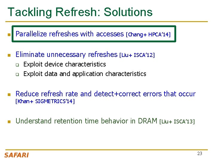
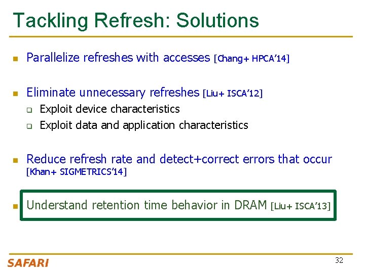
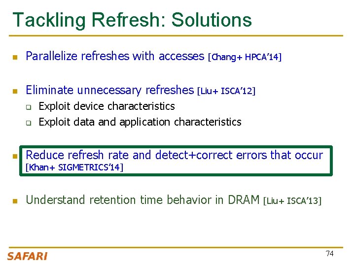
Tackling Refresh: Solutions n Parallelize refreshes with accesses n Eliminate unnecessary refreshes q q n [Chang+ HPCA’ 14] [Liu+ ISCA’ 12] Exploit device characteristics Exploit data and application characteristics Reduce refresh rate and detect+correct errors that occur [Khan+ SIGMETRICS’ 14] n Understand retention time behavior in DRAM [Liu+ ISCA’ 13] 23

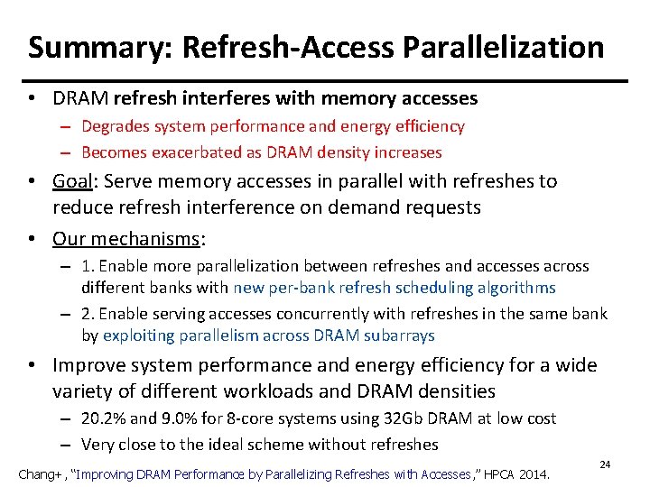
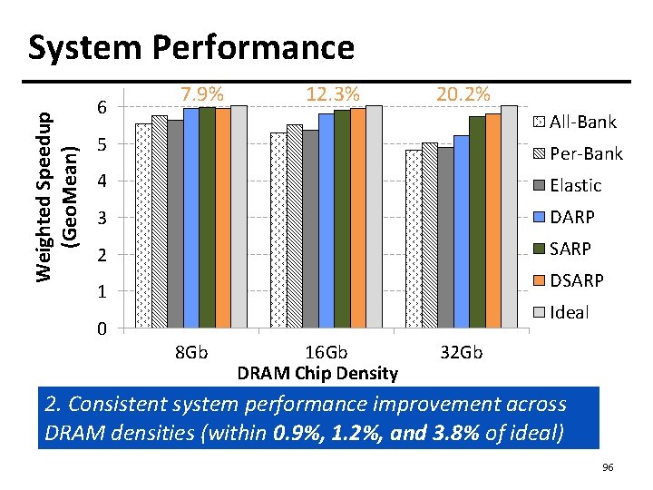
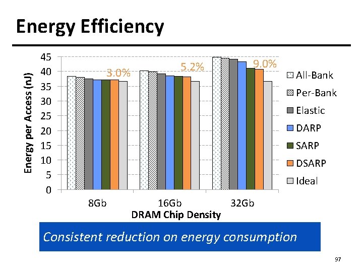
Summary: Refresh-Access Parallelization • DRAM refresh interferes with memory accesses – Degrades system performance and energy efficiency – Becomes exacerbated as DRAM density increases • Goal: Serve memory accesses in parallel with refreshes to reduce refresh interference on demand requests • Our mechanisms: – 1. Enable more parallelization between refreshes and accesses across different banks with new per-bank refresh scheduling algorithms – 2. Enable serving accesses concurrently with refreshes in the same bank by exploiting parallelism across DRAM subarrays • Improve system performance and energy efficiency for a wide variety of different workloads and DRAM densities – 20. 2% and 9. 0% for 8 -core systems using 32 Gb DRAM at low cost – Very close to the ideal scheme without refreshes Chang+, “Improving DRAM Performance by Parallelizing Refreshes with Accesses, ” HPCA 2014. 24

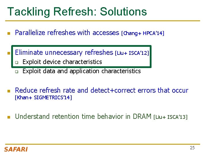
Tackling Refresh: Solutions n Parallelize refreshes with accesses n Eliminate unnecessary refreshes q q n [Chang+ HPCA’ 14] [Liu+ ISCA’ 12] Exploit device characteristics Exploit data and application characteristics Reduce refresh rate and detect+correct errors that occur [Khan+ SIGMETRICS’ 14] n Understand retention time behavior in DRAM [Liu+ ISCA’ 13] 25

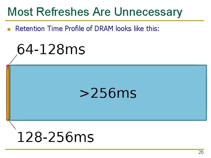
Most Refreshes Are Unnecessary n Retention Time Profile of DRAM looks like this: 26

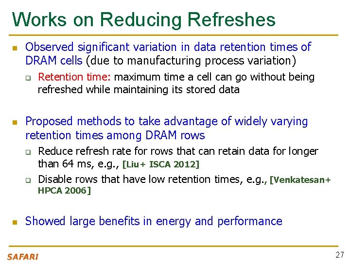
Works on Reducing Refreshes n Observed significant variation in data retention times of DRAM cells (due to manufacturing process variation) q n Retention time: maximum time a cell can go without being refreshed while maintaining its stored data Proposed methods to take advantage of widely varying retention times among DRAM rows q q Reduce refresh rate for rows that can retain data for longer than 64 ms, e. g. , [Liu+ ISCA 2012] Disable rows that have low retention times, e. g. , [Venkatesan+ HPCA 2006] n Showed large benefits in energy and performance 27
![An Example RAIDR Liu ISCA 2012 1 Profiling Profile the retention time of all An Example: RAIDR [Liu+, ISCA 2012] 1. Profiling: Profile the retention time of all](https://slidetodoc.com/presentation_image_h/3461c0226393c6d3c758b306433c3321/image-28.jpg)
An Example: RAIDR [Liu+, ISCA 2012] 1. Profiling: Profile the retention time of all DRAM rows 2. Binning: Store rows into bins by retention time use Bloom Filters for efficient and scalable storage 1. 25 KB storage in controller for 32 GB DRAM memory 3. Refreshing: Memory controller refreshes rows in different bins at different Can ratesreduce refreshes by ~75% probe Bloom Filters to determine rate of a row reduces energy consumption and refresh improves performance Liu et al. , “RAIDR: Retention-Aware Intelligent DRAM Refresh, ” ISCA 2012. 28

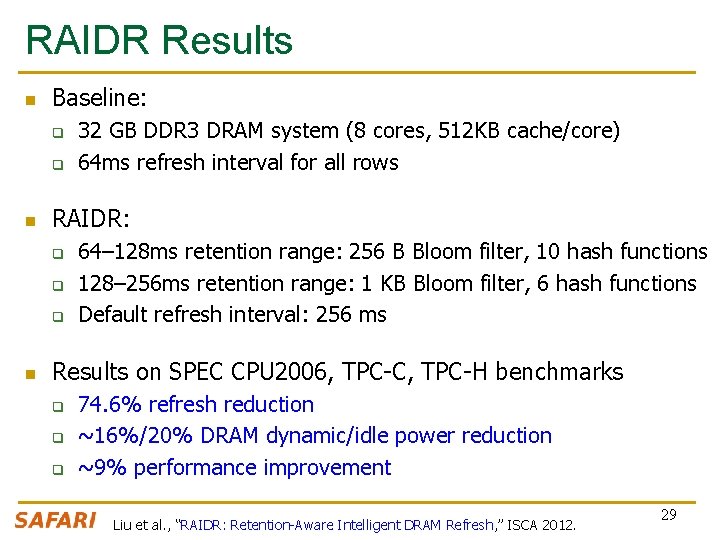
RAIDR Results n Baseline: q q n RAIDR: q q q n 32 GB DDR 3 DRAM system (8 cores, 512 KB cache/core) 64 ms refresh interval for all rows 64– 128 ms retention range: 256 B Bloom filter, 10 hash functions 128– 256 ms retention range: 1 KB Bloom filter, 6 hash functions Default refresh interval: 256 ms Results on SPEC CPU 2006, TPC-C, TPC-H benchmarks q q q 74. 6% refresh reduction ~16%/20% DRAM dynamic/idle power reduction ~9% performance improvement Liu et al. , “RAIDR: Retention-Aware Intelligent DRAM Refresh, ” ISCA 2012. 29

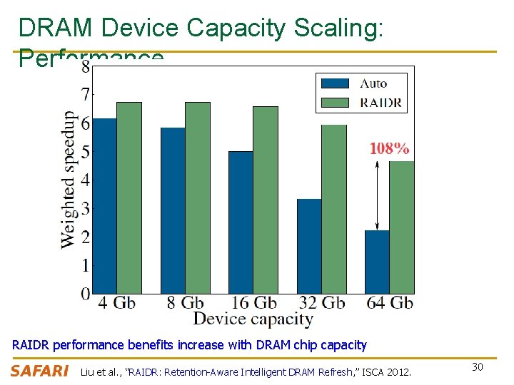
DRAM Device Capacity Scaling: Performance RAIDR performance benefits increase with DRAM chip capacity Liu et al. , “RAIDR: Retention-Aware Intelligent DRAM Refresh, ” ISCA 2012. 30

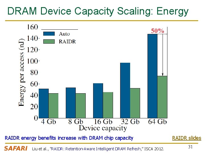
DRAM Device Capacity Scaling: Energy RAIDR energy benefits increase with DRAM chip capacity Liu et al. , “RAIDR: Retention-Aware Intelligent DRAM Refresh, ” ISCA 2012. RAIDR slides 31

Tackling Refresh: Solutions n Parallelize refreshes with accesses n Eliminate unnecessary refreshes q q n [Chang+ HPCA’ 14] [Liu+ ISCA’ 12] Exploit device characteristics Exploit data and application characteristics Reduce refresh rate and detect+correct errors that occur [Khan+ SIGMETRICS’ 14] n Understand retention time behavior in DRAM [Liu+ ISCA’ 13] 32

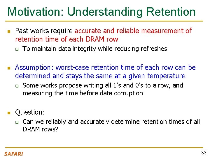
Motivation: Understanding Retention n Past works require accurate and reliable measurement of retention time of each DRAM row q n Assumption: worst-case retention time of each row can be determined and stays the same at a given temperature q n To maintain data integrity while reducing refreshes Some works propose writing all 1’s and 0’s to a row, and measuring the time before data corruption Question: q Can we reliably and accurately determine retention times of all DRAM rows? 33

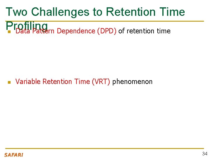
Two Challenges to Retention Time Profiling n Data Pattern Dependence (DPD) of retention time n Variable Retention Time (VRT) phenomenon 34

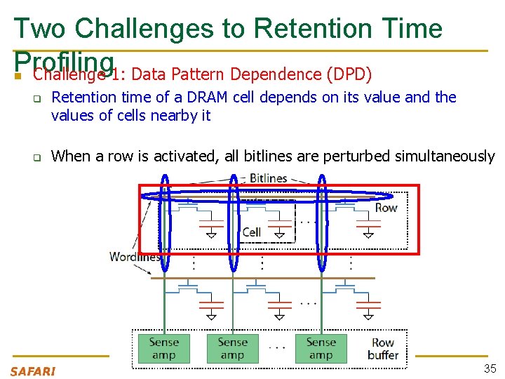
Two Challenges to Retention Time Profiling n Challenge 1: Data Pattern Dependence (DPD) q q Retention time of a DRAM cell depends on its value and the values of cells nearby it When a row is activated, all bitlines are perturbed simultaneously 35

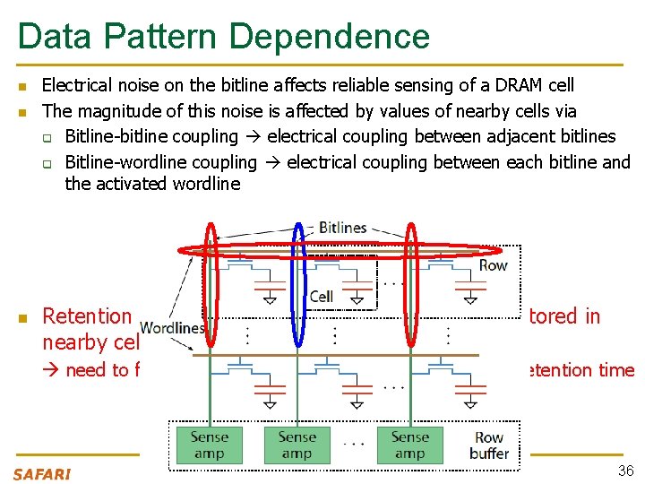
Data Pattern Dependence n n n Electrical noise on the bitline affects reliable sensing of a DRAM cell The magnitude of this noise is affected by values of nearby cells via q Bitline-bitline coupling electrical coupling between adjacent bitlines q Bitline-wordline coupling electrical coupling between each bitline and the activated wordline Retention time of a cell depends on data patterns stored in nearby cells need to find the worst data pattern to find worst-case retention time 36

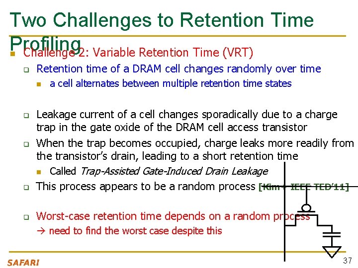
Two Challenges to Retention Time Profiling n Challenge 2: Variable Retention Time (VRT) q Retention time of a DRAM cell changes randomly over time n a cell alternates between multiple retention time states q Leakage current of a cell changes sporadically due to a charge trap in the gate oxide of the DRAM cell access transistor When the trap becomes occupied, charge leaks more readily from the transistor’s drain, leading to a short retention time n Called Trap-Assisted Gate-Induced Drain Leakage This process appears to be a random process [Kim+ IEEE TED’ 11] q Worst-case retention time depends on a random process q q need to find the worst case despite this 37
![Our Goal Liu ISCA 2013 n Analyze the retention time behavior of DRAM cells Our Goal [Liu+, ISCA 2013] n Analyze the retention time behavior of DRAM cells](https://slidetodoc.com/presentation_image_h/3461c0226393c6d3c758b306433c3321/image-38.jpg)
Our Goal [Liu+, ISCA 2013] n Analyze the retention time behavior of DRAM cells in modern commodity DRAM devices q n to aid the collection of accurate profile information Provide a comprehensive empirical investigation of two key challenges to retention time profiling q q Data Pattern Dependence (DPD) Variable Retention Time (VRT) Liu+, “An Experimental Study of Data Retention Behavior in Modern DRAM Devices, ” ISCA 2013. 38

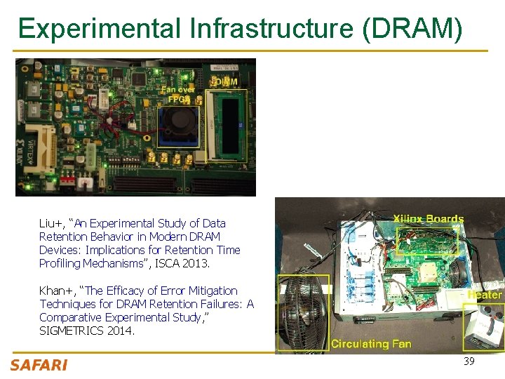
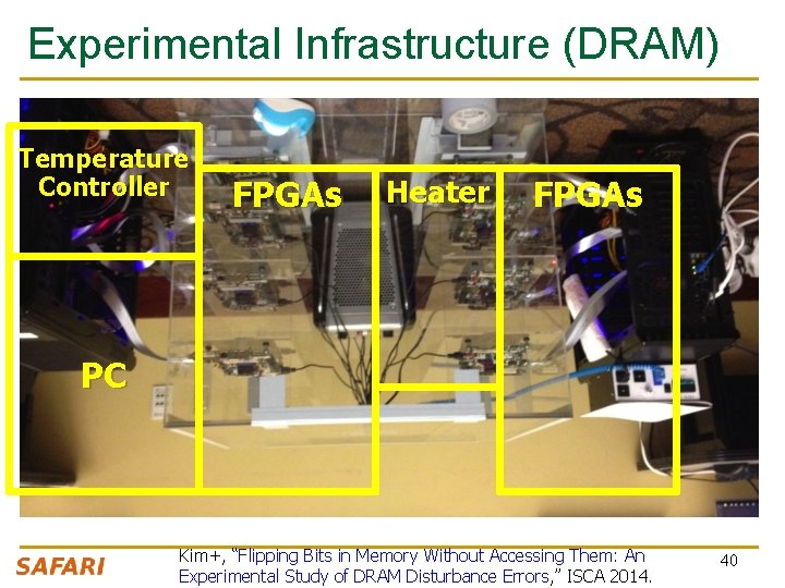
Experimental Infrastructure (DRAM) Liu+, “An Experimental Study of Data Retention Behavior in Modern DRAM Devices: Implications for Retention Time Profiling Mechanisms”, ISCA 2013. Khan+, “The Efficacy of Error Mitigation Techniques for DRAM Retention Failures: A Comparative Experimental Study, ” SIGMETRICS 2014. 39

Experimental Infrastructure (DRAM) Temperature Controller FPGAs Heater FPGAs PC Kim+, “Flipping Bits in Memory Without Accessing Them: An Experimental Study of DRAM Disturbance Errors, ” ISCA 2014. 40

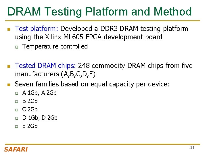
DRAM Testing Platform and Method n Test platform: Developed a DDR 3 DRAM testing platform using the Xilinx ML 605 FPGA development board q n n Temperature controlled Tested DRAM chips: 248 commodity DRAM chips from five manufacturers (A, B, C, D, E) Seven families based on equal capacity per device: q q q A 1 Gb, A 2 Gb B 2 Gb C 2 Gb D 1 Gb, D 2 Gb E 2 Gb 41

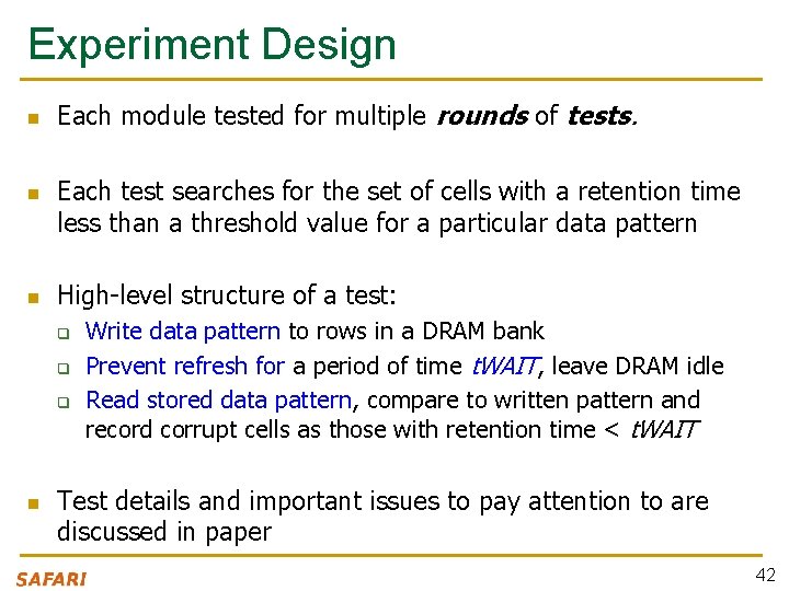
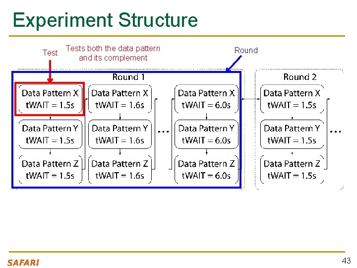
Experiment Design n Each module tested for multiple rounds of tests. Each test searches for the set of cells with a retention time less than a threshold value for a particular data pattern High-level structure of a test: q q q n Write data pattern to rows in a DRAM bank Prevent refresh for a period of time t. WAIT, leave DRAM idle Read stored data pattern, compare to written pattern and record corrupt cells as those with retention time < t. WAIT Test details and important issues to pay attention to are discussed in paper 42

Experiment Structure Tests both the data pattern and its complement Round 43

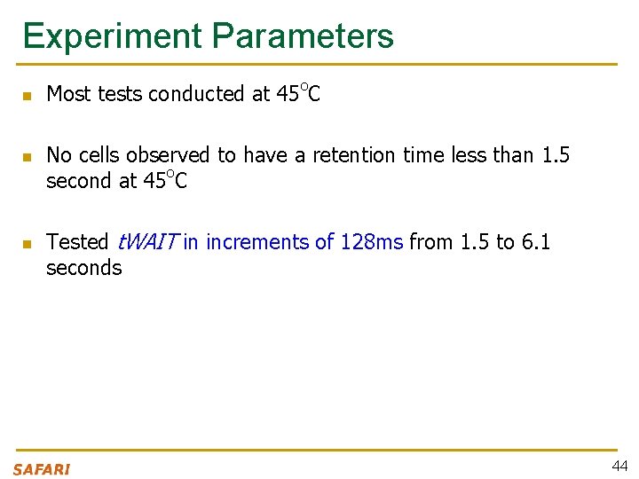
Experiment Parameters n n n Most tests conducted at 45 o. C No cells observed to have a retention time less than 1. 5 second at 45 o. C Tested t. WAIT in increments of 128 ms from 1. 5 to 6. 1 seconds 44

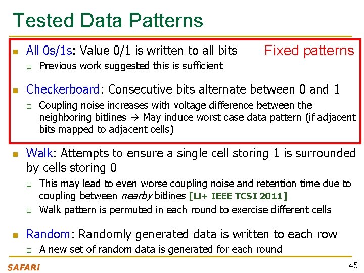
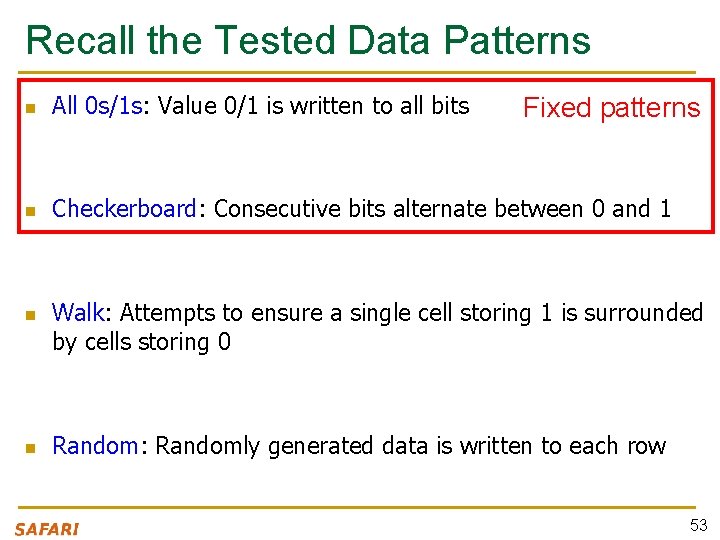
Tested Data Patterns n All 0 s/1 s: Value 0/1 is written to all bits q n Coupling noise increases with voltage difference between the neighboring bitlines May induce worst case data pattern (if adjacent bits mapped to adjacent cells) Walk: Attempts to ensure a single cell storing 1 is surrounded by cells storing 0 q q n Previous work suggested this is sufficient Checkerboard: Consecutive bits alternate between 0 and 1 q n Fixed patterns This may lead to even worse coupling noise and retention time due to coupling between nearby bitlines [Li+ IEEE TCSI 2011] Walk pattern is permuted in each round to exercise different cells Random: Randomly generated data is written to each row q A new set of random data is generated for each round 45

DRAM Retention Time: Results n Foundational Results q q n n n Temperature Dependence Retention Time Distribution Data Pattern Dependence: Analysis and Implications Variable Retention Time: Analysis and Implications Conclusions 46

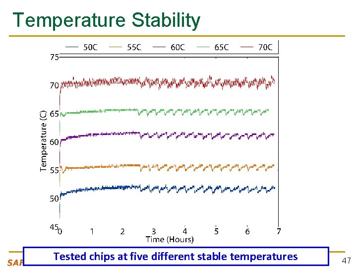
Temperature Stability Tested chips at five different stable temperatures 47

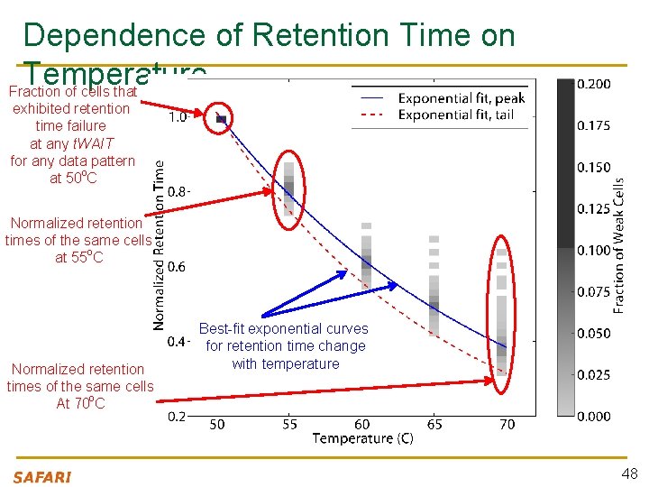
Dependence of Retention Time on Temperature Fraction of cells that exhibited retention time failure at any t. WAIT for any data pattern at 50 o. C Normalized retention times of the same cells at 55 o. C Normalized retention times of the same cells At 70 o. C Best-fit exponential curves for retention time change with temperature 48

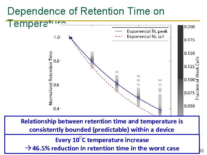
Dependence of Retention Time on Temperature Relationship between retention time and temperature is consistently bounded (predictable) within a device Every 10 o. C temperature increase 46. 5% reduction in retention time in the worst case 49

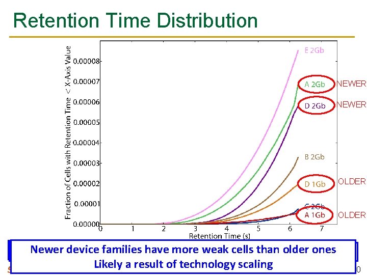
Retention Time Distribution NEWER OLDER Newer device have more weak cells than olderatones Minimum tested retention time ~1. 5 s atretention 45 C ~126 ms 85 C Very few cells exhibit the lowest times Shape of families the curve consistent with previous works Likely a result of technology scaling 50

DRAM Retention Time: Results n Foundational Results q q n n n Temperature Dependence Retention Time Distribution Data Pattern Dependence: Analysis and Implications Variable Retention Time: Analysis and Implications Conclusions 51

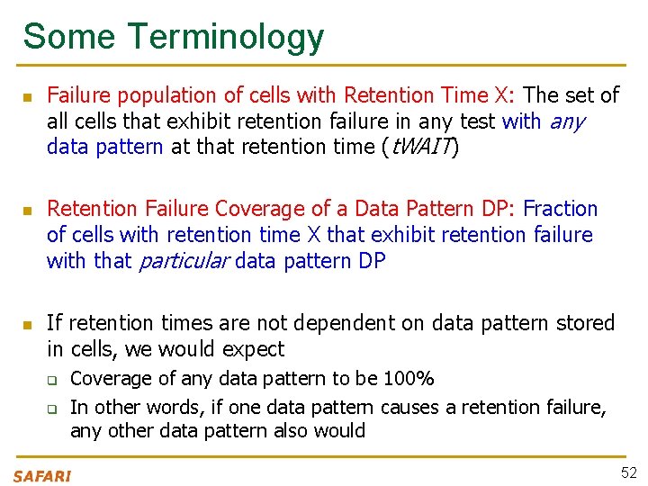
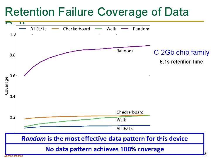
Some Terminology n n n Failure population of cells with Retention Time X: The set of all cells that exhibit retention failure in any test with any data pattern at that retention time (t. WAIT) Retention Failure Coverage of a Data Pattern DP: Fraction of cells with retention time X that exhibit retention failure with that particular data pattern DP If retention times are not dependent on data pattern stored in cells, we would expect q q Coverage of any data pattern to be 100% In other words, if one data pattern causes a retention failure, any other data pattern also would 52

Recall the Tested Data Patterns n All 0 s/1 s: Value 0/1 is written to all bits n Checkerboard: Consecutive bits alternate between 0 and 1 n n Fixed patterns Walk: Attempts to ensure a single cell storing 1 is surrounded by cells storing 0 Random: Randomly generated data is written to each row 53

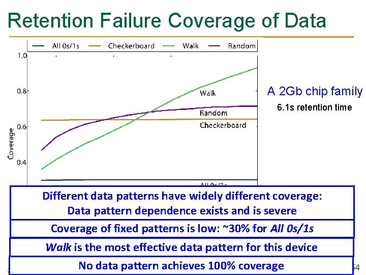
Retention Failure Coverage of Data Patterns A 2 Gb chip family 6. 1 s retention time Different data patterns have widely different coverage: Data pattern dependence exists and is severe Coverage of fixed patterns is low: ~30% for All 0 s/1 s Walk is the most effective data pattern for this device No data pattern achieves 100% coverage 54

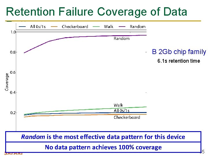
Retention Failure Coverage of Data Patterns B 2 Gb chip family 6. 1 s retention time Random is the most effective data pattern for this device No data pattern achieves 100% coverage 55

Retention Failure Coverage of Data Patterns C 2 Gb chip family 6. 1 s retention time Random is the most effective data pattern for this device No data pattern achieves 100% coverage 56

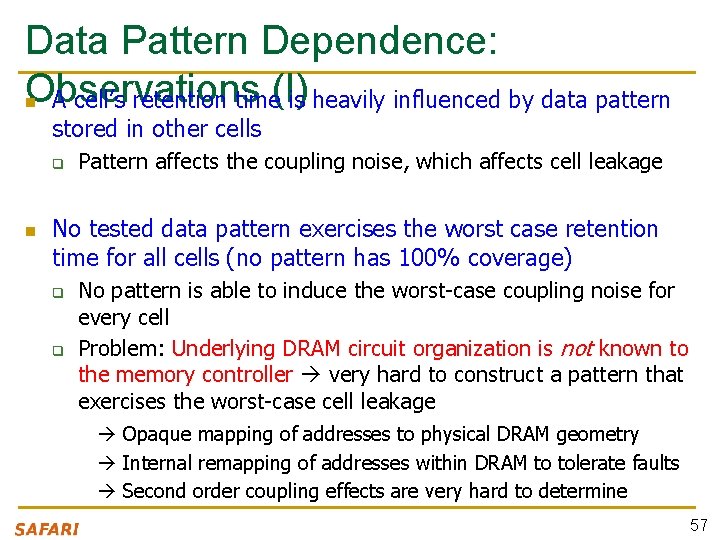
Data Pattern Dependence: Observations (I) n A cell’s retention time is heavily influenced by data pattern stored in other cells q n Pattern affects the coupling noise, which affects cell leakage No tested data pattern exercises the worst case retention time for all cells (no pattern has 100% coverage) q q No pattern is able to induce the worst-case coupling noise for every cell Problem: Underlying DRAM circuit organization is not known to the memory controller very hard to construct a pattern that exercises the worst-case cell leakage Opaque mapping of addresses to physical DRAM geometry Internal remapping of addresses within DRAM to tolerate faults Second order coupling effects are very hard to determine 57

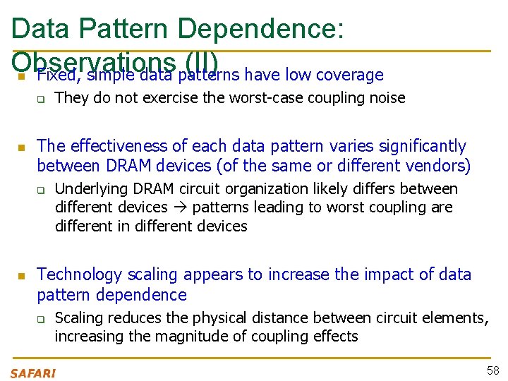
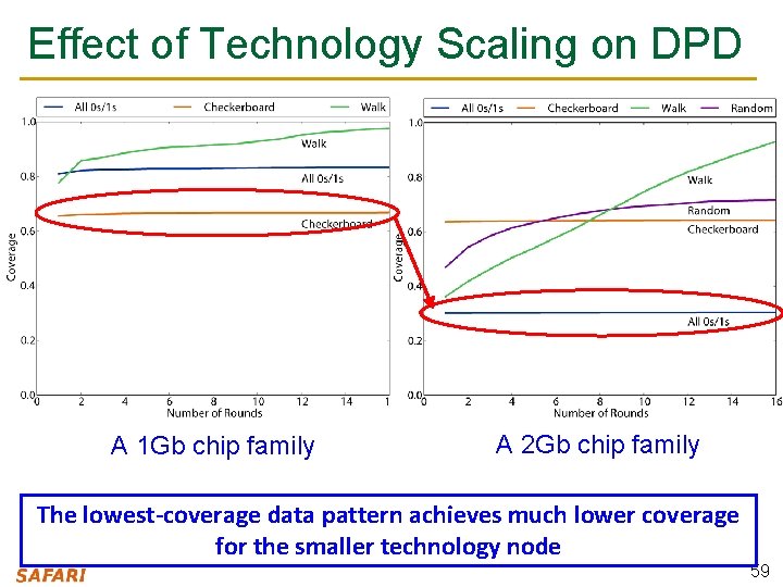
Data Pattern Dependence: Observations (II) n Fixed, simple data patterns have low coverage q n The effectiveness of each data pattern varies significantly between DRAM devices (of the same or different vendors) q n They do not exercise the worst-case coupling noise Underlying DRAM circuit organization likely differs between different devices patterns leading to worst coupling are different in different devices Technology scaling appears to increase the impact of data pattern dependence q Scaling reduces the physical distance between circuit elements, increasing the magnitude of coupling effects 58

Effect of Technology Scaling on DPD A 1 Gb chip family A 2 Gb chip family The lowest-coverage data pattern achieves much lower coverage for the smaller technology node 59

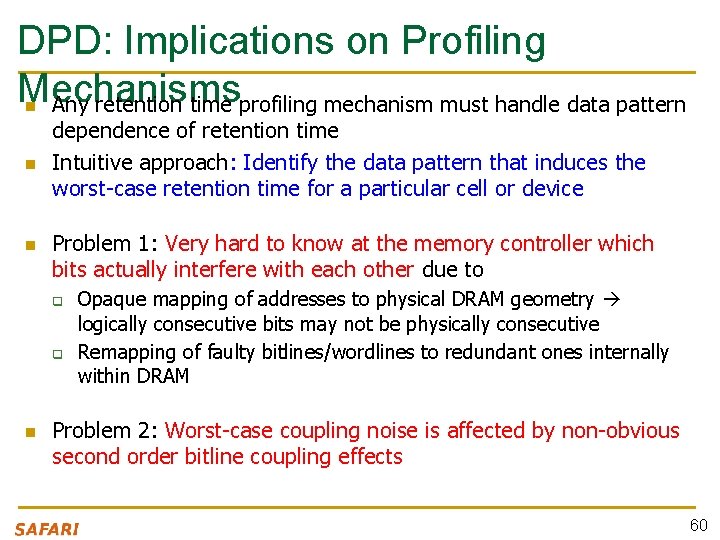
DPD: Implications on Profiling Mechanisms Any retention time profiling mechanism must handle data pattern n dependence of retention time Intuitive approach: Identify the data pattern that induces the worst-case retention time for a particular cell or device Problem 1: Very hard to know at the memory controller which bits actually interfere with each other due to q q n Opaque mapping of addresses to physical DRAM geometry logically consecutive bits may not be physically consecutive Remapping of faulty bitlines/wordlines to redundant ones internally within DRAM Problem 2: Worst-case coupling noise is affected by non-obvious second order bitline coupling effects 60

DRAM Retention Time: Results n Foundational Results q q n n n Temperature Dependence Retention Time Distribution Data Pattern Dependence: Analysis and Implications Variable Retention Time: Analysis and Implications Conclusions 61

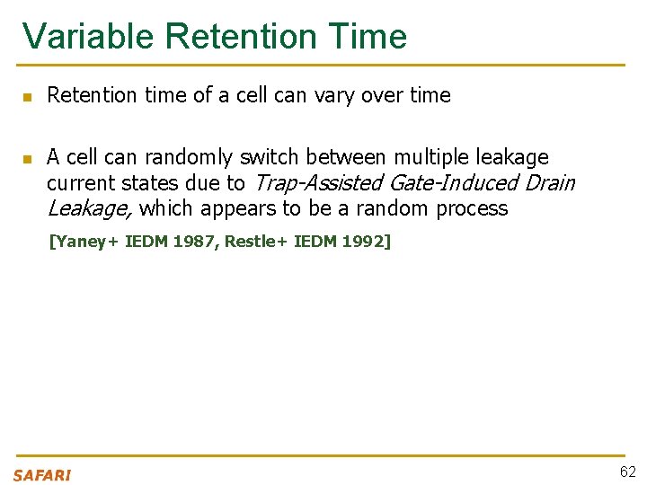
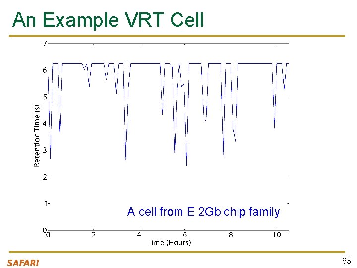
Variable Retention Time n n Retention time of a cell can vary over time A cell can randomly switch between multiple leakage current states due to Trap-Assisted Gate-Induced Drain Leakage, which appears to be a random process [Yaney+ IEDM 1987, Restle+ IEDM 1992] 62

An Example VRT Cell A cell from E 2 Gb chip family 63

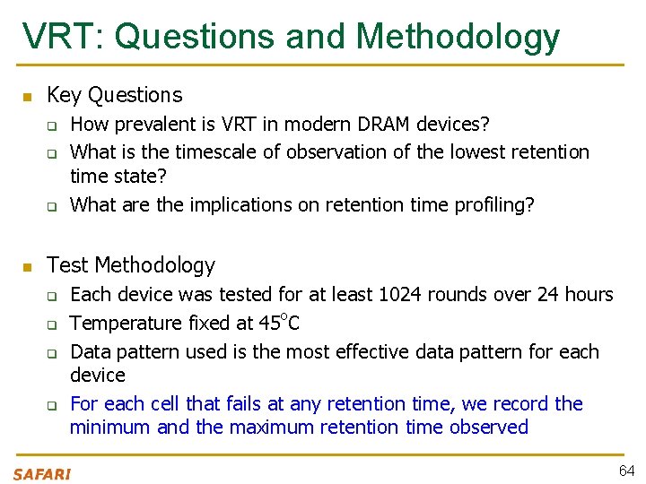
VRT: Questions and Methodology n Key Questions q q q n How prevalent is VRT in modern DRAM devices? What is the timescale of observation of the lowest retention time state? What are the implications on retention time profiling? Test Methodology q q Each device was tested for at least 1024 rounds over 24 hours Temperature fixed at 45 o. C Data pattern used is the most effective data pattern for each device For each cell that fails at any retention time, we record the minimum and the maximum retention time observed 64

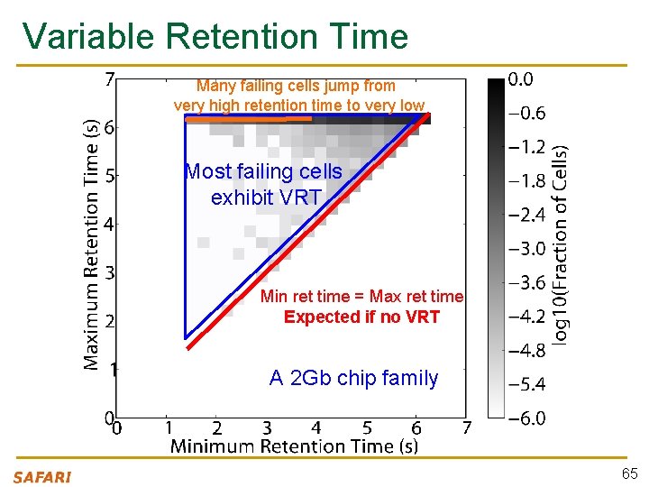
Variable Retention Time Many failing cells jump from very high retention time to very low Most failing cells exhibit VRT Min ret time = Max ret time Expected if no VRT A 2 Gb chip family 65

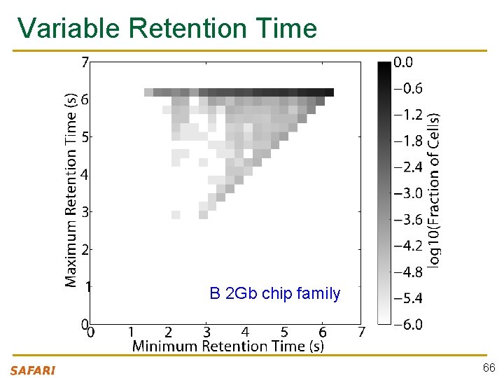
Variable Retention Time B 2 Gb chip family 66

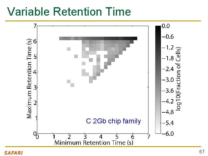
Variable Retention Time C 2 Gb chip family 67

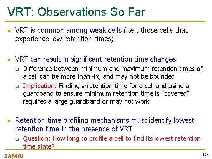
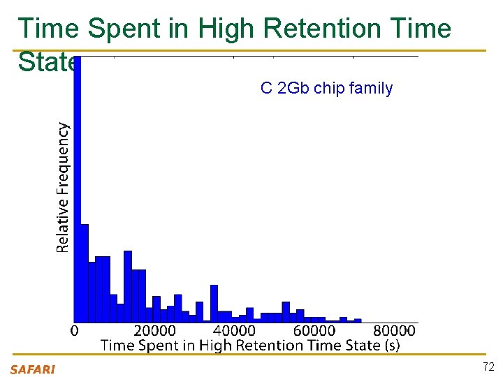
VRT: Observations So Far n n VRT is common among weak cells (i. e. , those cells that experience low retention times) VRT can result in significant retention time changes q q n Difference between minimum and maximum retention times of a cell can be more than 4 x, and may not be bounded Implication: Finding a retention time for a cell and using a guardband to ensure minimum retention time is “covered” requires a large guardband or may not work Retention time profiling mechanisms must identify lowest retention time in the presence of VRT q Question: How long to profile a cell to find its lowest retention time state? 68

Time Between Retention Time State Changes n How much time does a cell spend in a high retention state before switching to the minimum observed retention time state? 69

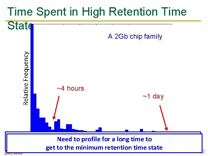
Time Spent in High Retention Time State A 2 Gb chip family ~4 hours ~1 day Time scale at which a cell switches retention time state Need to profile fortoa the longlow time to long (~retention 1 day or longer) getcan to be thevery minimum time state 70

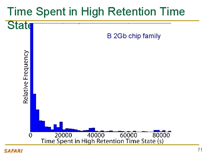
Time Spent in High Retention Time State B 2 Gb chip family 71

Time Spent in High Retention Time State C 2 Gb chip family 72

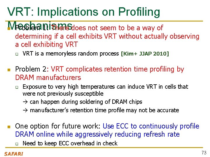
VRT: Implications on Profiling Mechanisms n Problem 1: There does not seem to be a way of determining if a cell exhibits VRT without actually observing a cell exhibiting VRT q n Problem 2: VRT complicates retention time profiling by DRAM manufacturers q n VRT is a memoryless random process [Kim+ JJAP 2010] Exposure to very high temperatures can induce VRT in cells that were not previously susceptible can happen during soldering of DRAM chips manufacturer’s retention time profile may not be accurate One option for future work: Use ECC to continuously profile DRAM online while aggressively reducing refresh rate q Need to keep ECC overhead in check 73

Tackling Refresh: Solutions n Parallelize refreshes with accesses n Eliminate unnecessary refreshes q q n [Chang+ HPCA’ 14] [Liu+ ISCA’ 12] Exploit device characteristics Exploit data and application characteristics Reduce refresh rate and detect+correct errors that occur [Khan+ SIGMETRICS’ 14] n Understand retention time behavior in DRAM [Liu+ ISCA’ 13] 74

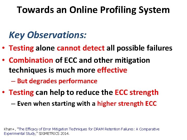
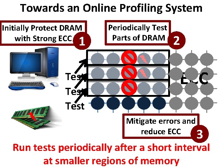
Towards an Online Profiling System Key Observations: • Testing alone cannot detect all possible failures • Combination of ECC and other mitigation techniques is much more effective – But degrades performance • Testing can help to reduce the ECC strength – Even when starting with a higher strength ECC Khan+, “The Efficacy of Error Mitigation Techniques for DRAM Retention Failures: A Comparative Experimental Study, ” SIGMETRICS 2014.

Towards an Online Profiling System Initially Protect DRAM with Strong ECC 1 Test Periodically Test Parts of DRAM 2 ECC Mitigate errors and reduce ECC 3 Run tests periodically after a short interval at smaller regions of memory

Agenda n n n Major Trends Affecting Main Memory The DRAM Scaling Problem Refresh as a Limiter of DRAM Scaling Some Solution Directions and Challenges Summary 77

Summary and Conclusions n DRAM refresh is a critical challenge q n in scaling DRAM technology efficiently to higher capacities Discussed several promising solution directions q q q Parallelize refreshes with accesses [Chang+ HPCA’ 14] Eliminate unnecessary refreshes [Liu+ ISCA’ 12] Reduce refresh rate and detect+correct errors that occur [Khan+ SIGMETRICS’ 14] n Examined properties of retention time behavior n Many avenues for overcoming DRAM refresh challenges q q q [Liu+ ISCA’ 13] Handling DPD/VRT phenomena Enabling online retention time profiling and error mitigation Exploiting application behavior 78

Referenced Papers n All are available at http: //users. ece. cmu. edu/~omutlu/projects. htm 79

Related Videos and Course Materials n Computer Architecture Lecture Videos on Youtube q n Computer Architecture Course Materials q n http: //www. ece. cmu. edu/~ece 447/s 13/doku. php? id=schedule Advanced Computer Architecture Course Materials q n https: //www. youtube. com/playlist? list=PL 5 PHm 2 jkk. Xmid. JOd 59 R Eog 9 j. Dn. PDTG 6 IJ http: //www. ece. cmu. edu/~ece 740/f 13/doku. php? id=schedule Advanced Computer Architecture Lecture Videos on Youtube q https: //www. youtube. com/playlist? list=PL 5 PHm 2 jkk. Xmg. DN 1 PLw OY_t. Gt. Ulynny. V 6 D 80

Thank you. Feel free to email me with any questions & feedback onur@cmu. edu http: //users. ece. cmu. edu/~omutlu/

Understanding and Overcoming Challenges of DRAM Refresh Onur Mutlu onur@cmu. edu June 30, 2014 Extreme Scale Scientific Computing Workshop

Additional Slides

84

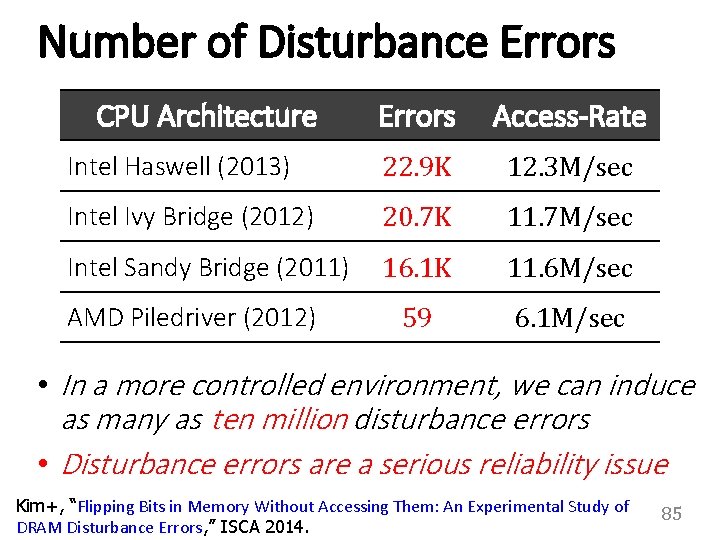
Number of Disturbance Errors CPU Architecture Errors Access-Rate Intel Haswell (2013) 22. 9 K 12. 3 M/sec Intel Ivy Bridge (2012) 20. 7 K 11. 7 M/sec Intel Sandy Bridge (2011) 16. 1 K 11. 6 M/sec 59 6. 1 M/sec AMD Piledriver (2012) • In a more controlled environment, we can induce as many as ten million disturbance errors • Disturbance errors are a serious reliability issue Kim+, “Flipping Bits in Memory Without Accessing Them: An Experimental Study of DRAM Disturbance Errors, ” ISCA 2014. 85
![Summary and Conclusions ISCA 13 n n DRAM refresh is a critical challenge in Summary and Conclusions [ISCA’ 13] n n DRAM refresh is a critical challenge in](https://slidetodoc.com/presentation_image_h/3461c0226393c6d3c758b306433c3321/image-86.jpg)
Summary and Conclusions [ISCA’ 13] n n DRAM refresh is a critical challenge in scaling DRAM technology efficiently to higher capacities and smaller feature sizes Understanding the retention time of modern DRAM devices can enable old or new methods to reduce the impact of refresh q n We presented the first work that comprehensively examines data retention behavior in modern commodity DRAM devices q n Characterized 248 devices from five manufacturers Key findings: Retention time of a cell significantly depends on data pattern stored in other cells (data pattern dependence) and changes over time via a random process (variable retention time) q n Many mechanisms require accurate and reliable retention time profiles Discussed the underlying reasons and provided suggestions Future research on retention time profiling should solve the challenges posed by the DPD and VRT phenomena 86

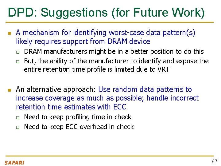
DPD: Suggestions (for Future Work) n A mechanism for identifying worst-case data pattern(s) likely requires support from DRAM device q q n DRAM manufacturers might be in a better position to do this But, the ability of the manufacturer to identify and expose the entire retention time profile is limited due to VRT An alternative approach: Use random data patterns to increase coverage as much as possible; handle incorrect retention time estimates with ECC q q Need to keep profiling time in check Need to keep ECC overhead in check 87

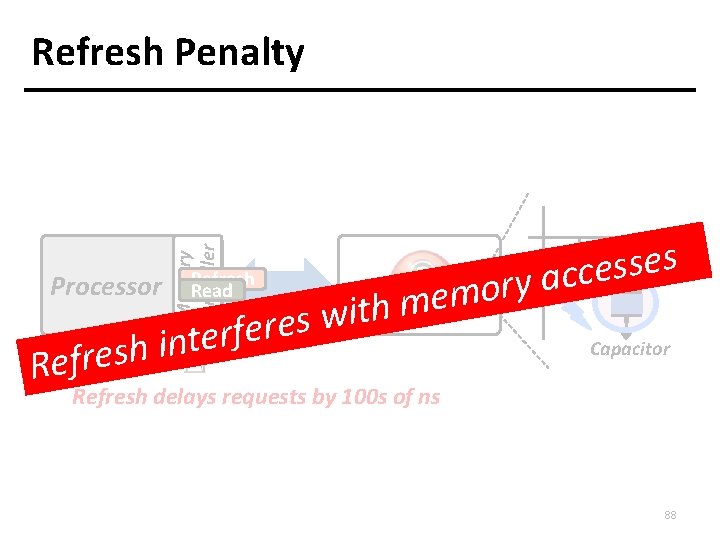
Refresh Penalty Memory Controller s e s s e DRAMmory acc Processor Refresh Read e Data m h t i w s e r e f r e t Capacitor n i h s Refre Access transistor Refresh delays requests by 100 s of ns 88

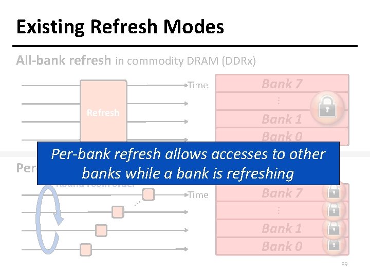
Existing Refresh Modes All-bank refresh in commodity DRAM (DDRx) Time Bank 7 … Refresh Bank 1 Bank 0 Per-bank refresh allows accesses to other Per-bank refresh mobile DRAM (LPDDRx) banksinwhile a bank is refreshing Round-robin order Time Bank 7 … Bank 1 Bank 0 89 …

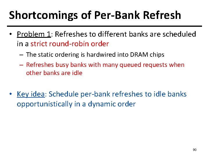
Shortcomings of Per-Bank Refresh • Problem 1: Refreshes to different banks are scheduled in a strict round-robin order – The static ordering is hardwired into DRAM chips – Refreshes busy banks with many queued requests when other banks are idle • Key idea: Schedule per-bank refreshes to idle banks opportunistically in a dynamic order 90

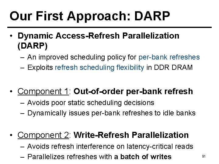
Our First Approach: DARP • Dynamic Access-Refresh Parallelization (DARP) – An improved scheduling policy for per-bank refreshes – Exploits refresh scheduling flexibility in DDR DRAM • Component 1: Out-of-order per-bank refresh – Avoids poor static scheduling decisions – Dynamically issues per-bank refreshes to idle banks • Component 2: Write-Refresh Parallelization – Avoids refresh interference on latency-critical reads – Parallelizes refreshes with a batch of writes 91

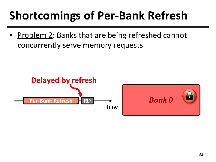
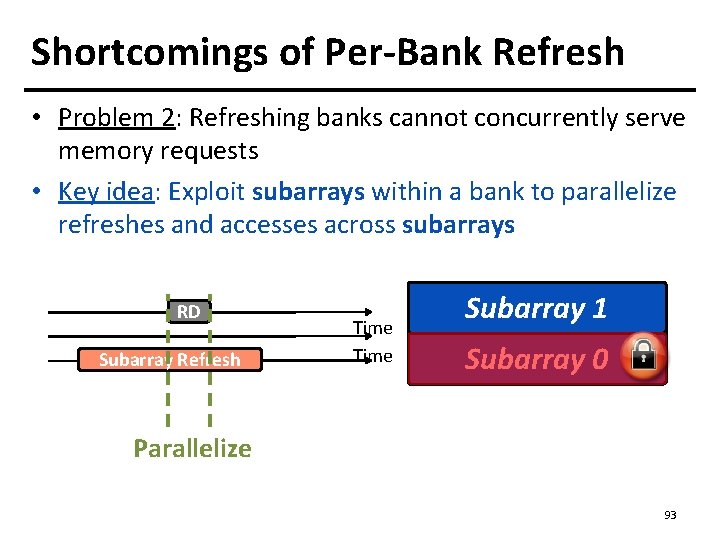
Shortcomings of Per-Bank Refresh • Problem 2: Banks that are being refreshed cannot concurrently serve memory requests Delayed by refresh Per-Bank Refresh RD Time Bank 0 92

Shortcomings of Per-Bank Refresh • Problem 2: Refreshing banks cannot concurrently serve memory requests • Key idea: Exploit subarrays within a bank to parallelize refreshes and accesses across subarrays RD Subarray Refresh Time Subarray 1 Bank 0 Subarray 0 Parallelize 93

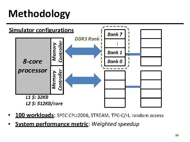
Methodology Bank 1 Bank 0 Memory Controller DDR 3 Rank Bank 7 … 8 -core processor Memory Controller Simulator configurations L 1 $: 32 KB L 2 $: 512 KB/core • 100 workloads: SPEC CPU 2006, STREAM, TPC-C/H, random access • System performance metric: Weighted speedup 94
![Comparison Points Allbank refresh DDR 3 LPDDR 3 Perbank refresh LPDDR Comparison Points • All-bank refresh [DDR 3, LPDDR 3, …] • Per-bank refresh [LPDDR](https://slidetodoc.com/presentation_image_h/3461c0226393c6d3c758b306433c3321/image-95.jpg)
Comparison Points • All-bank refresh [DDR 3, LPDDR 3, …] • Per-bank refresh [LPDDR 3] • Elastic refresh [Stuecheli et al. , MICRO ‘ 10]: – Postpones refreshes by a time delay based on the predicted rank idle time to avoid interference on memory requests – Proposed to schedule all-bank refreshes without exploiting per-bank refreshes – Cannot parallelize refreshes and accesses within a rank • Ideal (no refresh) 95

Weighted Speedup (Geo. Mean) System Performance 6 7. 9% 12. 3% 20. 2% All-Bank 5 Per-Bank 4 Elastic 3 DARP 2 SARP DSARP 1 0 Ideal 8 Gb 16 Gb DRAM Chip Density 32 Gb 1. Both DARPsystem & SARP provide performance and 2. Consistent performance improvementgains across DRAM densities 0. 9%, 1. 2%, and 3. 8% of ideal) combining them(within (DSARP) improves even more 96

Energy per Access (n. J) Energy Efficiency 45 40 35 30 25 20 15 10 5 0 3. 0% 5. 2% 9. 0% All-Bank Per-Bank Elastic DARP SARP DSARP Ideal 8 Gb 16 Gb 32 Gb DRAM Chip Density Consistent reduction on energy consumption 97

Another Talk: NAND Flash Scaling Challenges n n n Cai+, “Error Patterns in MLC NAND Flash Memory: Measurement, Characterization, and Analysis, ” DATE 2012. Cai+, “Flash Correct-and-Refresh: Retention-Aware Error Management for Increased Flash Memory Lifetime, ” ICCD 2012. Cai+, “Threshold Voltage Distribution in MLC NAND Flash Memory: Characterization, Analysis and Modeling, ” DATE 2013. Cai+, “Error Analysis and Retention-Aware Error Management for NAND Flash Memory, ” Intel Tech Journal 2013. Cai+, “Program Interference in MLC NAND Flash Memory: Characterization, Modeling, and Mitigation, ” ICCD 2013. Cai+, “Neighbor-Cell Assisted Error Correction for MLC NAND Flash Memories, ” SIGMETRICS 2014. 98

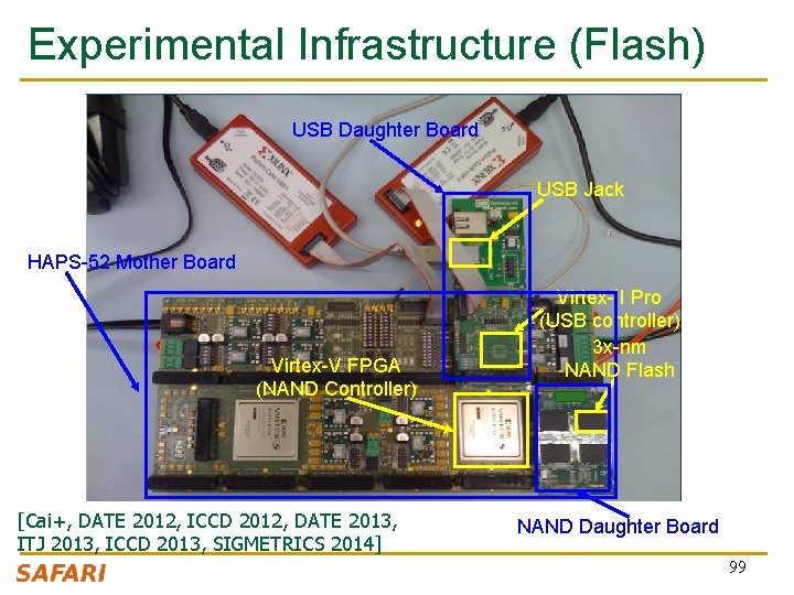
Experimental Infrastructure (Flash) USB Daughter Board USB Jack HAPS-52 Mother Board Virtex-V FPGA (NAND Controller) [Cai+, DATE 2012, ICCD 2012, DATE 2013, ITJ 2013, ICCD 2013, SIGMETRICS 2014] Virtex-II Pro (USB controller) 3 x-nm NAND Flash NAND Daughter Board 99