Optimizing DRAM Timing for the CommonCase AdaptiveLatency DRAM



- Slides: 45

Optimizing DRAM Timing for the Common-Case Adaptive-Latency DRAM Donghyuk Lee Yoongu Kim, Gennady Pekhimenko, Samira Khan, Vivek Seshadri, Kevin Chang, Onur Mutlu

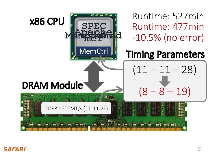
Runtime: 527 min x 86 CPU SPEC Runtime: 477 min Apache GUPS Memcached Parsec -10. 5% (no error) mcf Mem. Ctrl Timing Parameters (11 – 28) DRAM Module (8 – 19) DDR 3 1600 MT/s (11 -11 -28) 2

Reducing DRAM Timing Why can we reduce DRAM timing parameters without any errors? 3

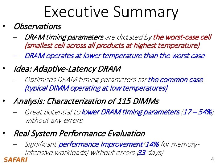
Executive Summary • Observations – DRAM timing parameters are dictated by the worst-case cell (smallest cell across all products at highest temperature) – DRAM operates at lower temperature than the worst case • Idea: Adaptive-Latency DRAM – Optimizes DRAM timing parameters for the common case (typical DIMM operating at low temperatures) • Analysis: Characterization of 115 DIMMs – Great potential to lower DRAM timing parameters (17 – 54%) without any errors • Real System Performance Evaluation – Significant performance improvement (14% for memoryintensive workloads) without errors (33 days) 4

1. DRAM Operation Basics 2. Reasons for Timing Margin in DRAM 3. Key Observations 4. Adaptive-Latency DRAM 5. DRAM Characterization 6. Real System Performance Evaluation 5

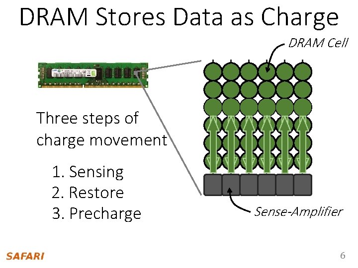
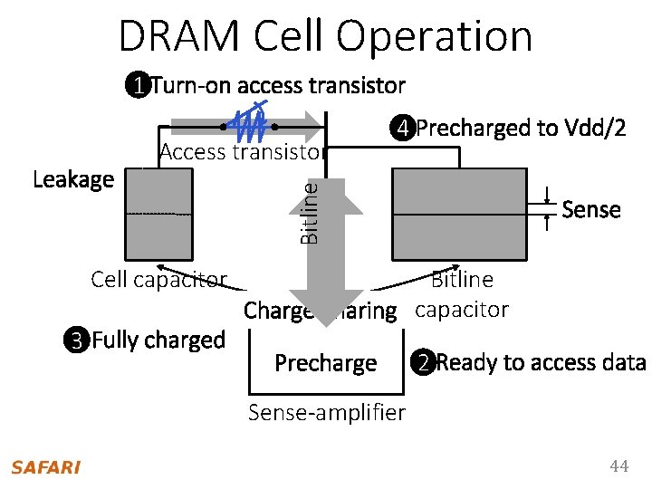
DRAM Stores Data as Charge DRAM Cell Three steps of charge movement 1. Sensing 2. Restore 3. Precharge Sense-Amplifier 6

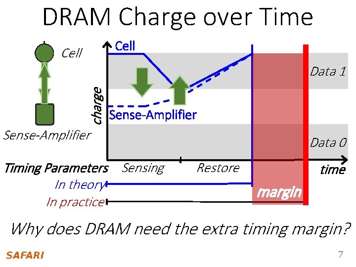
DRAM Charge over Time Cell charge Data 1 Sense-Amplifier Timing Parameters Sensing In theory In practice Data 0 Restore time margin Why does DRAM need the extra timing margin? 7

1. DRAM Operation Basics 2. Reasons for Timing Margin in DRAM 3. Key Observations 4. Adaptive-Latency DRAM 5. DRAM Characterization 6. Real System Performance Evaluation 8

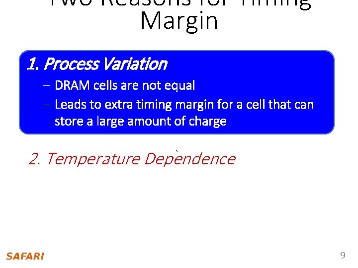
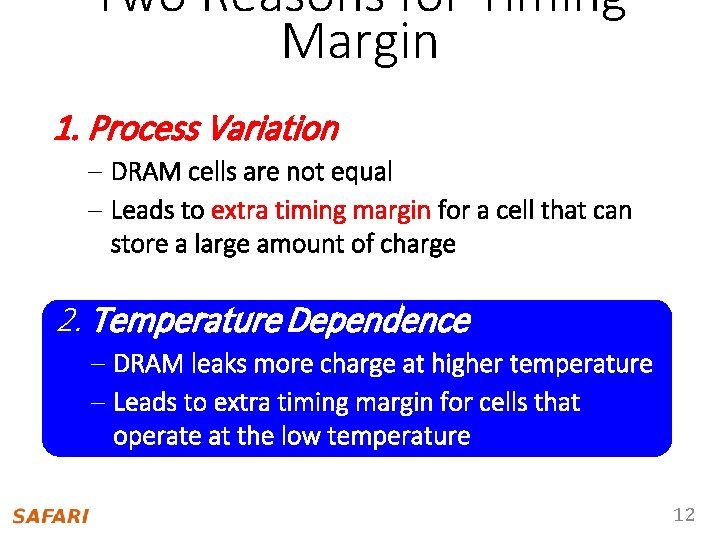
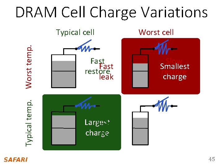
Two Reasons for Timing Margin 1. Process Variation – DRAM cells are not equal – Leads to extra timing margin for acellthatcan store asmall largeamountofofcharge 2. Temperature Dependence ` – DRAM leaks more charge at higher temperature – Leads to extra timing margin when operating at low temperature 9

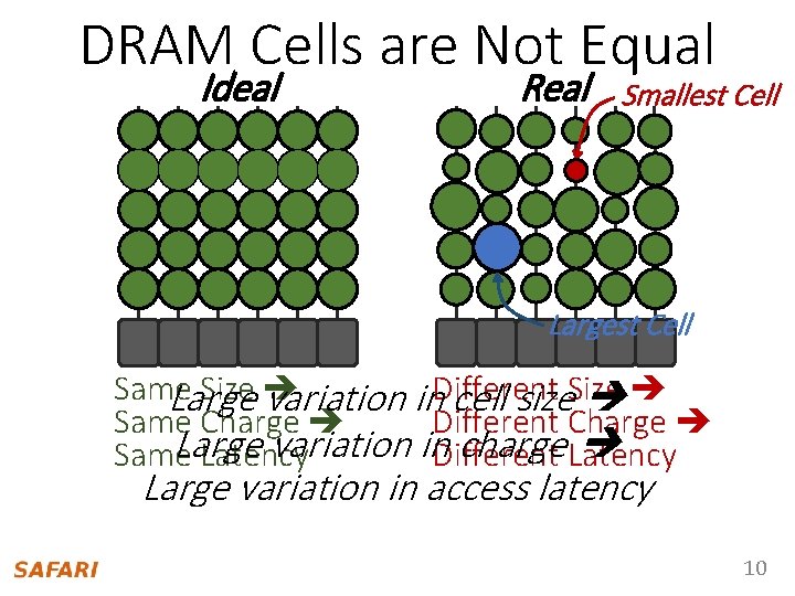
DRAM Cells are Not Equal Ideal Real Smallest Cell Largest Cell Same Size Large variation in. Different cell size. Size Same Charge Different Charge Large variation in. Different charge Latency Same Latency Large variation in access latency 10

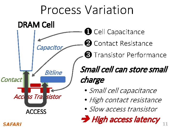
Process Variation DRAM Cell Contact ❶ Cell Capacitance Capacitor ❷ Contact Resistance ❸ Transistor Performance Bitline Small cell can store small charge Access Transistor ACCESS • Small cell capacitance • High contact resistance • Slow access transistor High access latency 11

Two Reasons for Timing Margin 1. Process Variation – DRAM cells are not equal – Leads to extra timing margin for a cell that can store a large amount of charge 2. Temperature Dependence ` – DRAM leaks more charge at higher temperature – Leads to extra timing margin for cells that operate at the low hightemperature 12

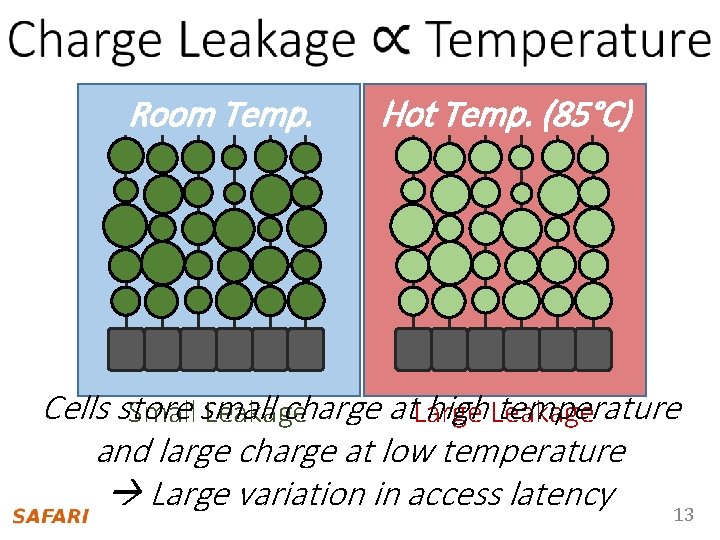
Room Temp. Hot Temp. (85°C) Cells store charge at. Large high Leakage temperature Small small Leakage and large charge at low temperature Large variation in access latency 13

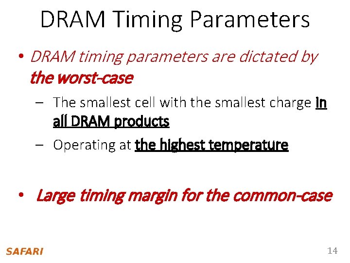
DRAM Timing Parameters • DRAM timing parameters are dictated by the worst-case – The smallest cell with the smallest charge in all DRAM products – Operating at the highest temperature • Large timing margin for the common-case 14

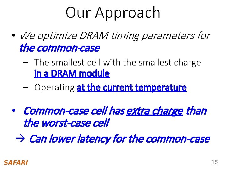
Our Approach • We optimize DRAM timing parameters for the common-case – The smallest cell with the smallest charge in a DRAM module – Operating at the current temperature • Common-case cell has extra charge than the worst-case cell à Can lower latency for the common-case 15

1. DRAM Operation Basics 2. Reasons for Timing Margin in DRAM 3. Key Observations 4. Adaptive-Latency DRAM 5. DRAM Characterization 6. Real System Performance Evaluation 16

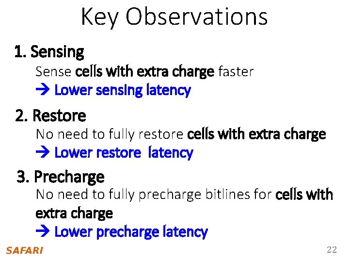
Key Observations 1. Sensing Sense cells with extra charge faster Lower sensing latency 2. Restore No need to fully restore cells with extra charge Lower restore latency 3. Precharge No need to fully precharge bitlines for cells with extra charge Lower precharge latency 17

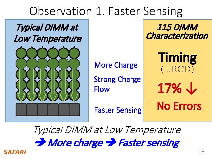
Observation 1. Faster Sensing 115 DIMM Characterization Typical DIMM at Low Temperature More Charge Timing (t. RCD) Strong Charge Flow 17% ↓ Faster Sensing No Errors Typical DIMM at Low Temperature More charge Faster sensing 18

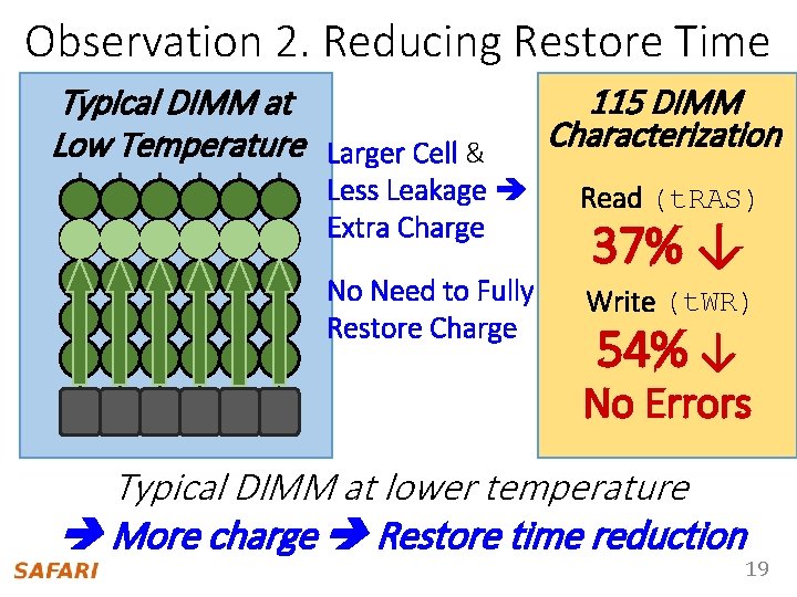
Observation 2. Reducing Restore Time Typical DIMM at Low Temperature Larger Cell & 115 DIMM Characterization Less Leakage Extra Charge Read (t. RAS) No Need to Fully Restore Charge Write (t. WR) 37% ↓ 54% ↓ No Errors Typical DIMM at lower temperature More charge Restore time reduction 19

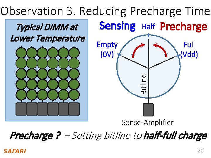
Observation 3. Reducing Precharge Time Sensing Half Precharge Empty (0 V) Full (Vdd) Bitline Typical DIMM at Lower Temperature Sense-Amplifier Precharge ? – Setting bitline to half-full charge 20

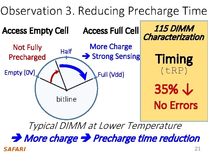
Observation 3. Reducing Precharge Time Access Empty Cell Not Fully Precharged Half Empty (0 V) Access Full Cell More Charge Strong Sensing Full (Vdd) bitline 115 DIMM Characterization Timing (t. RP) 35% ↓ No Errors Typical DIMM at Lower Temperature More charge Precharge time reduction 21

Key Observations 1. Sensing Sense cells with extra charge faster Lower sensing latency 2. Restore No need to fully restore cells with extra charge Lower restore latency 3. Precharge No need to fully precharge bitlines for cells with extra charge Lower precharge latency 22

1. DRAM Operation Basics 2. Reasons for Timing Margin in DRAM 3. Key Observations 4. Adaptive-Latency DRAM 5. DRAM Characterization 6. Real System Performance Evaluation 23

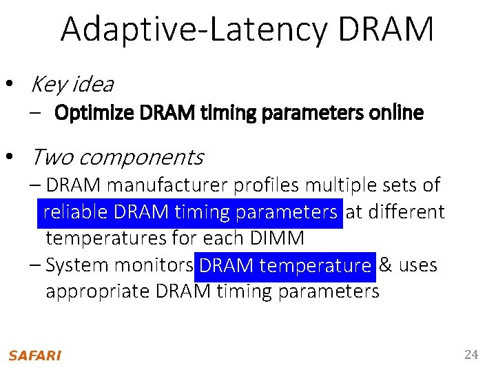
Adaptive-Latency DRAM • Key idea – Optimize DRAM timing parameters online • Two components – DRAM manufacturer profiles multiple sets of reliable DRAM timing parameters at different reliable temperatures for each DIMM – System monitors DRAM temperature & uses appropriate DRAM timing parameters 24

1. DRAM Operation Basics 2. Reasons for Timing Margin in DRAM 3. Key Observations 4. Adaptive-Latency DRAM 5. DRAM Characterization 6. Real System Performance Evaluation 25

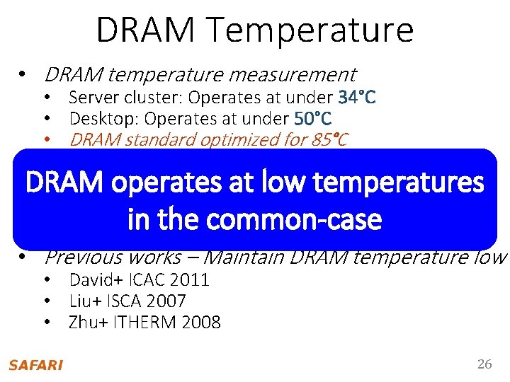
DRAM Temperature • DRAM temperature measurement • Server cluster: Operates at under 34°C • Desktop: Operates at under 50°C • DRAM standard optimized for 85°C • DRAM Previousoperates works – DRAM temperature is low at low temperatures • El-Sayed+ SIGMETRICS 2012 in 2007 the common-case • Liu+ ISCA • Previous works – Maintain DRAM temperature low • David+ ICAC 2011 • Liu+ ISCA 2007 • Zhu+ ITHERM 2008 26

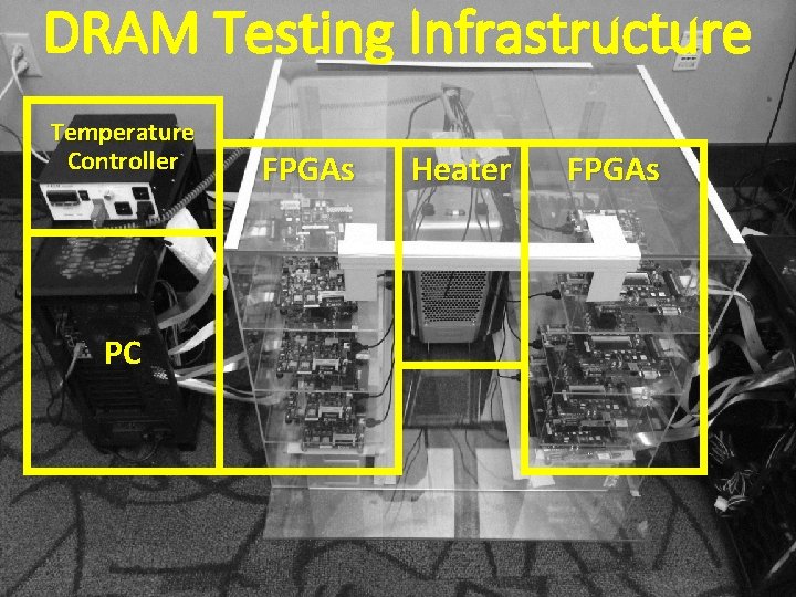
DRAM Testing Infrastructure Temperature Controller FPGAs Heater FPGAs PC 27

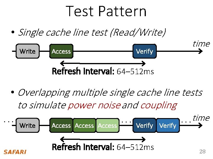
Test Pattern • Single cache line test (Read/Write) Write Access Verify time Refresh Interval: 64– 512 ms • Overlapping multiple single cache line tests to simulate power noise and coupling. . . Write Access . . . Verify Refresh Interval: 64– 512 ms . . . time 28

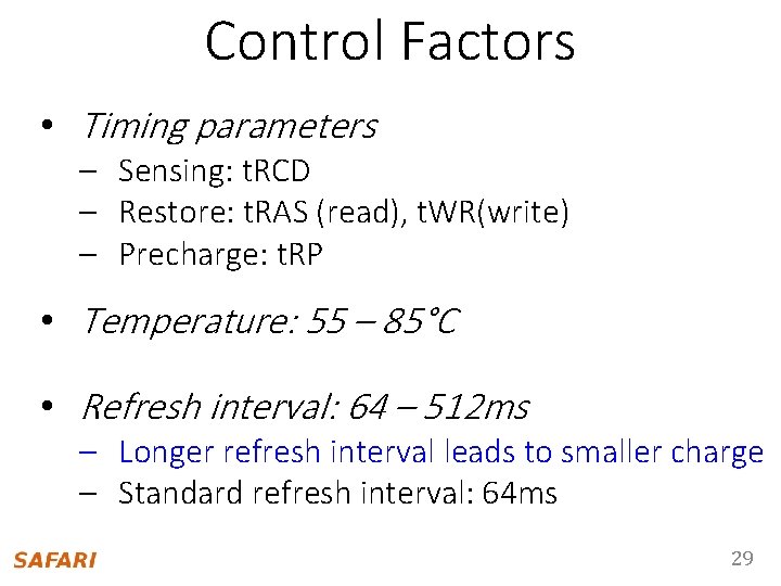
Control Factors • Timing parameters – Sensing: t. RCD – Restore: t. RAS (read), t. WR(write) – Precharge: t. RP • Temperature: 55 – 85°C • Refresh interval: 64 – 512 ms – Longer refresh interval leads to smaller charge – Standard refresh interval: 64 ms 29

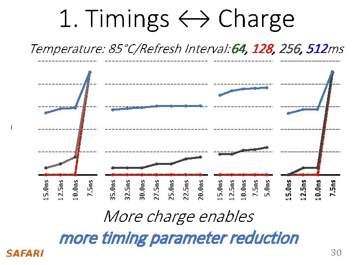
1. Timings ↔ Charge Temperature: 85°C/Refresh Interval: 64, 128, 256, 512 ms 105 Restore (Read) Sensing Precharge 103 102 7. 5 ns 10. 0 ns 12. 5 ns 15. 0 ns 12. 5 ns 10. 0 ns 7. 5 ns 5. 0 ns 20. 0 ns 22. 5 ns 25. 0 ns 27. 5 ns 30. 0 ns 32. 5 ns 35. 0 ns 7. 5 ns 10. 0 ns 0 12. 5 ns 10 15. 0 ns Errors 104 Restore (Write) More charge enables more timing parameter reduction 30

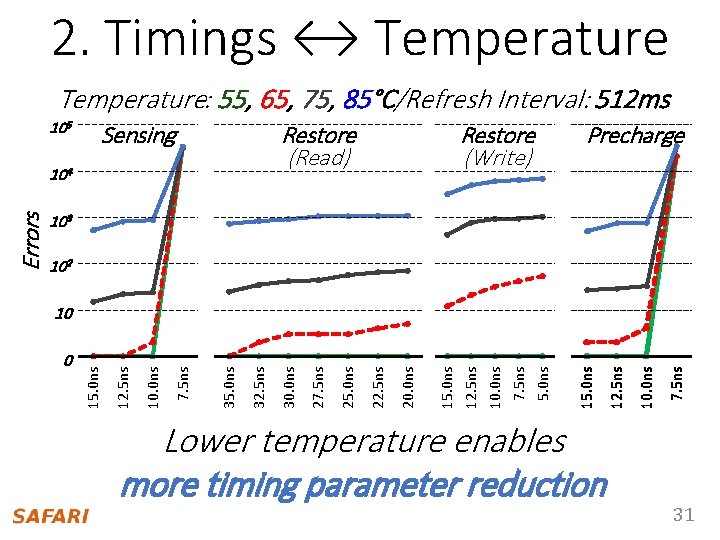
2. Timings ↔ Temperature: 55, 65, 75, 85°C/Refresh Interval: 512 ms 105 Restore (Read) Sensing Precharge 103 102 7. 5 ns 10. 0 ns 12. 5 ns 15. 0 ns 12. 5 ns 10. 0 ns 7. 5 ns 5. 0 ns 20. 0 ns 22. 5 ns 25. 0 ns 27. 5 ns 30. 0 ns 32. 5 ns 35. 0 ns 7. 5 ns 10. 0 ns 0 12. 5 ns 10 15. 0 ns Errors 104 Restore (Write) Lower temperature enables more timing parameter reduction 31

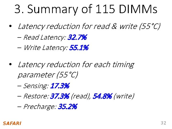
3. Summary of 115 DIMMs • Latency reduction for read & write (55°C) – Read Latency: 32. 7% – Write Latency: 55. 1% • Latency reduction for each timing parameter (55°C) – Sensing: 17. 3% – Restore: 37. 3% (read), 54. 8% (write) – Precharge: 35. 2% 32

1. DRAM Operation Basics 2. Reasons for Timing Margin in DRAM 3. Key Observations 4. Adaptive-Latency DRAM 5. DRAM Characterization 6. Real System Performance Evaluation 33

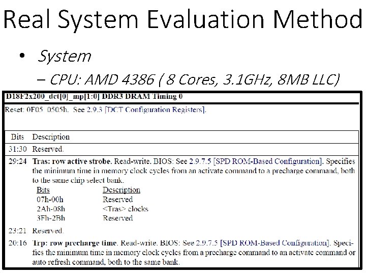
Real System Evaluation Method • System – CPU: AMD 4386 ( 8 Cores, 3. 1 GHz, 8 MB LLC) – DRAM: 4 GByte DDR 3 -1600 (800 Mhz Clock) – OS: Linux – Storage: 128 GByte SSD • Workload – 35 applications from SPEC, STREAM, Parsec, Memcached, Apache, GUPS 34

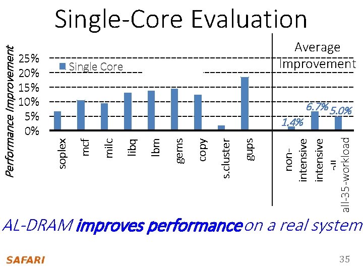
Single Core Average Improvement Multi Core 6. 7% 5. 0% nonintensive allall-35 -workloads gups s. cluster copy gems lbm libq milc 1. 4% mcf 25% 20% 15% 10% 5% 0% soplex Performance Improvement Single-Core Evaluation AL-DRAM improves performance on a real system 35

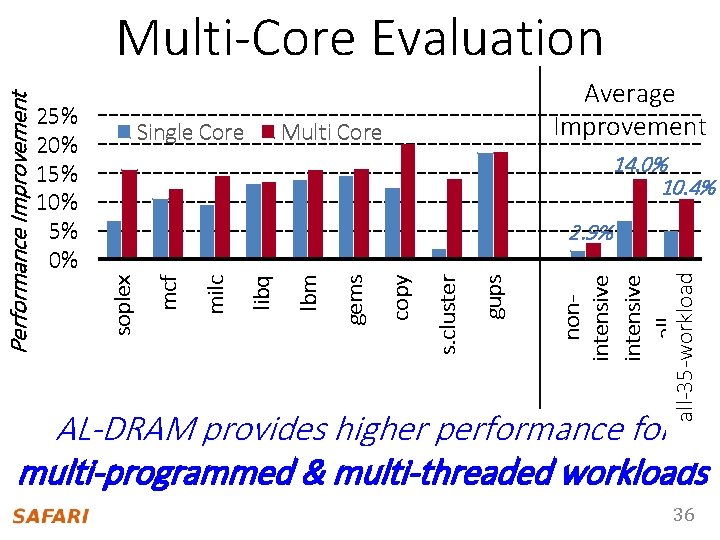
Single Core Average Improvement Multi Core 14. 0% 10. 4% nonintensive allall-35 -workloads gups s. cluster copy gems lbm libq milc 2. 9% mcf 25% 20% 15% 10% 5% 0% soplex Performance Improvement Multi-Core Evaluation AL-DRAM provides higher performance for multi-programmed & multi-threaded workloads 36

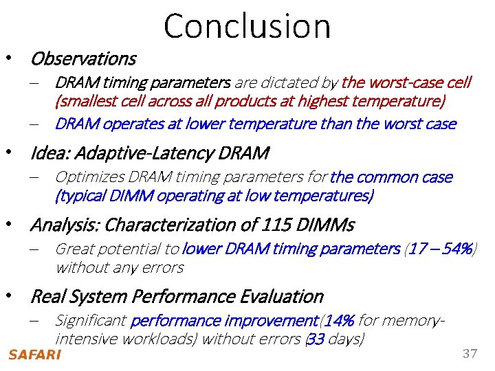
• Observations Conclusion – DRAM timing parameters are dictated by the worst-case cell (smallest cell across all products at highest temperature) – DRAM operates at lower temperature than the worst case • Idea: Adaptive-Latency DRAM – Optimizes DRAM timing parameters for the common case (typical DIMM operating at low temperatures) • Analysis: Characterization of 115 DIMMs – Great potential to lower DRAM timing parameters (17 – 54%) without any errors • Real System Performance Evaluation – Significant performance improvement (14% for memoryintensive workloads) without errors (33 days) 37

Optimizing DRAM Timing for the Common-Case Adaptive-Latency DRAM Donghyuk Lee Yoongu Kim, Gennady Pekhimenko, Samira Khan, Vivek Seshadri, Kevin Chang, Onur Mutlu

Backup Slides 39

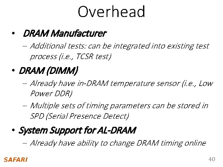
Overhead • DRAM Manufacturer – Additional tests: can be integrated into existing test process (i. e. , TCSR test) • DRAM (DIMM) – Already have in-DRAM temperature sensor (i. e. , Low Power DDR) – Multiple sets of timing parameters can be stored in SPD (Serial Presence Detect) • System Support for AL-DRAM – Already have ability to change DRAM timing online 40

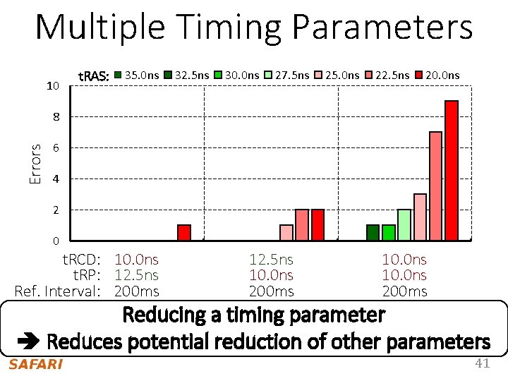
Multiple Timing Parameters 10 t. RAS: 35. 0 ns 32. 5 ns 30. 0 ns 27. 5 ns 25. 0 ns 22. 5 ns 20. 0 ns Errors 8 6 4 2 0 A t. RCD: 10. 0 ns t. RP: 12. 5 ns Ref. Interval: 200 ms B 12. 5 ns 10. 0 ns 200 ms C 10. 0 ns 200 ms Reducing a timing parameter Reduces potential reduction of other parameters 41

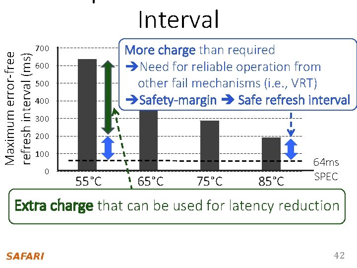
Maximum error-free refresh interval (ms) Interval More charge than required Need for reliable operation from other fail mechanisms (i. e. , VRT) Safety-margin Safe refresh interval 700 600 500 400 300 200 100 0 55°C 75°C 65°C Temperature (°C) 85°C 64 ms SPEC Extra charge that can be used for latency reduction 42

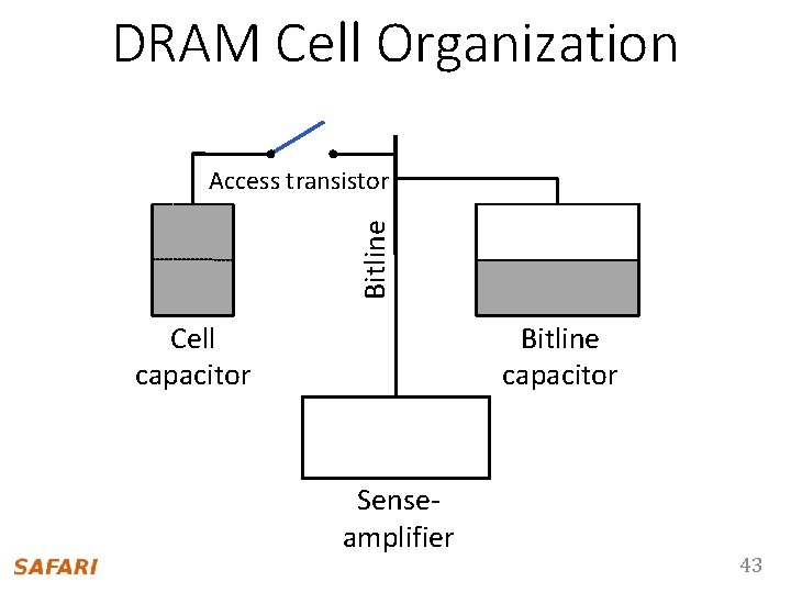
DRAM Cell Organization Bitline Access transistor Cell capacitor Bitline capacitor Senseamplifier 43

DRAM Cell Operation 1 Turn-on access transistor Cell capacitor 3 Fully charged Bitline Leakage Access transistor 4 Precharged to Vdd/2 Sense Bitline Charge-sharing capacitor Amplify Precharge 2 Ready to access data Sense-amplifier 44

DRAM Cell Charge Variations Worst temp. Fast restore leak Typical temp. Typical cell Slowly Largest leak charge Worst cell Slow Smallest restore charge 45