Types of RAM Dynamic RAM DRAM Most commonly

- Slides: 39

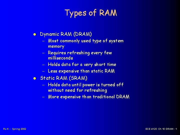
Types of RAM Dynamic RAM (DRAM) – Most commonly used type of system memory – Requires refreshing every few milliseconds – Holds data for a very short time – Less expensive than static RAM Static RAM (SRAM) – Holds data until power is turned off without need for refreshing – More expensive than traditional DRAM RLH - Spring 2002 ECE 4120 Ch 10 DRAM - 1

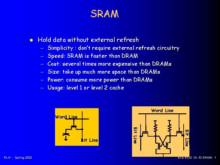
SRAM Hold data without external refresh – – – Simplicity : don’t require external refresh circuitry Speed: SRAM is faster than DRAM Cost: several times more expensive than DRAMs Size: take up much more space than DRAMs Power: consume more power than DRAMs Usage: level 1 or level 2 cache Word Line Bit Line RLH - Spring 2002 Bit Line ECE 4120 Ch 10 DRAM - 1

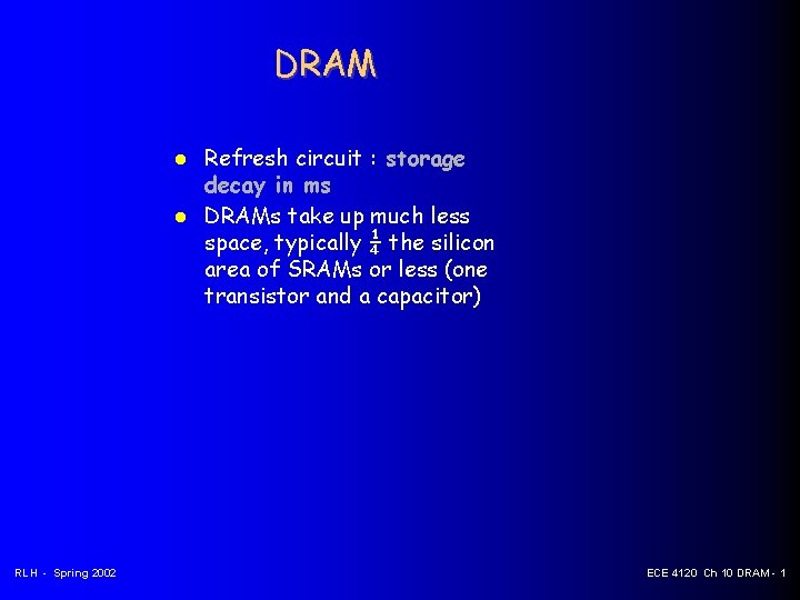
DRAM RLH - Spring 2002 Refresh circuit : storage decay in ms DRAMs take up much less space, typically ¼ the silicon area of SRAMs or less (one transistor and a capacitor) ECE 4120 Ch 10 DRAM - 1

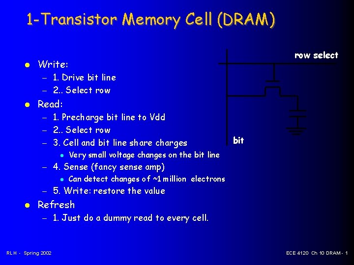
1 -Transistor Memory Cell (DRAM) row select Write: – 1. Drive bit line – 2. . Select row Read: – 1. Precharge bit line to Vdd – 2. . Select row – 3. Cell and bit line share charges bit Very small voltage changes on the bit line – 4. Sense (fancy sense amp) Can detect changes of ~1 million electrons – 5. Write: restore the value Refresh – 1. Just do a dummy read to every cell. RLH - Spring 2002 ECE 4120 Ch 10 DRAM - 1

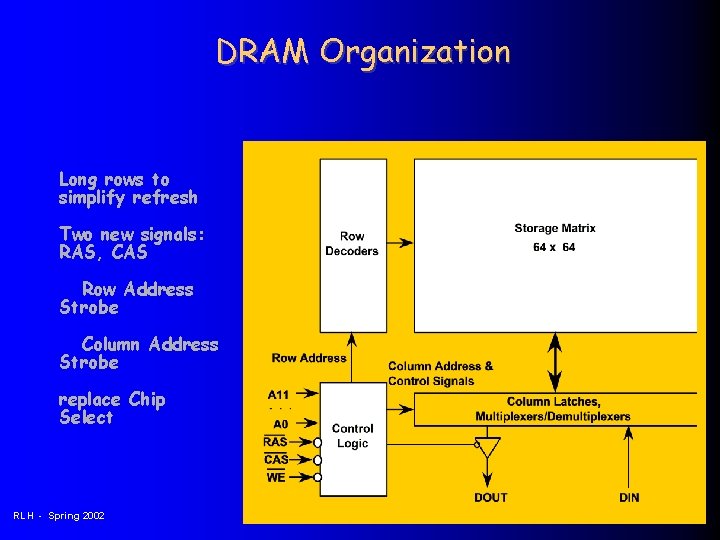
DRAM Organization Long rows to simplify refresh Two new signals: RAS, CAS Row Address Strobe Column Address Strobe replace Chip Select RLH - Spring 2002 ECE 4120 Ch 10 DRAM - 1

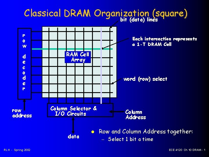
Classical DRAM Organization (square) bit (data) lines r o w d e c o d e r row address Each intersection represents a 1 -T DRAM Cell Array word (row) select Column Selector & I/O Circuits data RLH - Spring 2002 Column Address Row and Column Address together: – Select 1 bit a time ECE 4120 Ch 10 DRAM - 1

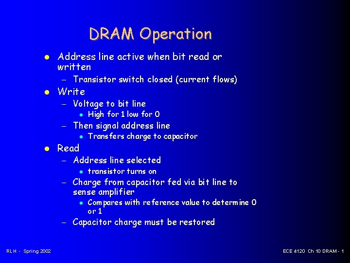
DRAM Operation Address line active when bit read or written – Transistor switch closed (current flows) Write – Voltage to bit line High for 1 low for 0 – Then signal address line Read Transfers charge to capacitor – Address line selected transistor turns on – Charge from capacitor fed via bit line to sense amplifier Compares with reference value to determine 0 or 1 – Capacitor charge must be restored RLH - Spring 2002 ECE 4120 Ch 10 DRAM - 1

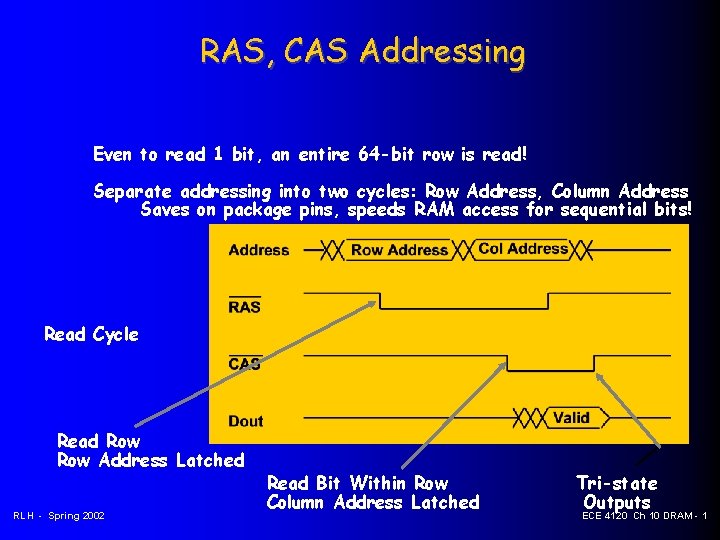
RAS, CAS Addressing Even to read 1 bit, an entire 64 -bit row is read! Separate addressing into two cycles: Row Address, Column Address Saves on package pins, speeds RAM access for sequential bits! Read Cycle Read Row Address Latched RLH - Spring 2002 Read Bit Within Row Column Address Latched Tri-state Outputs ECE 4120 Ch 10 DRAM - 1

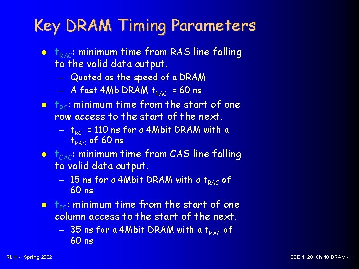
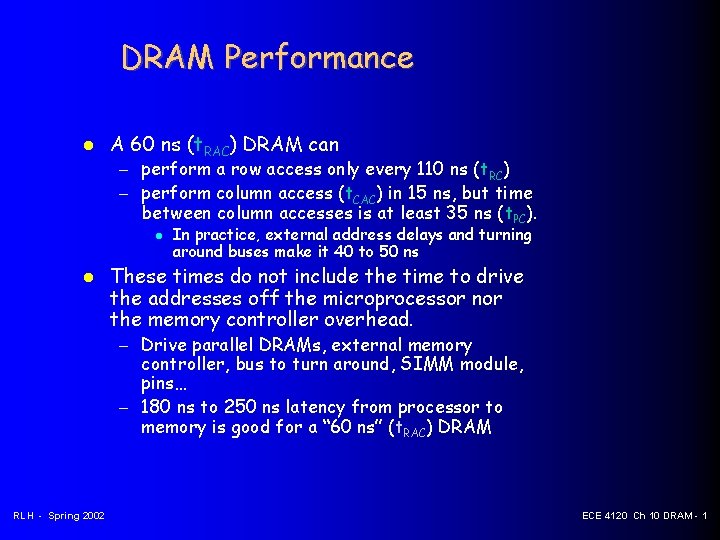
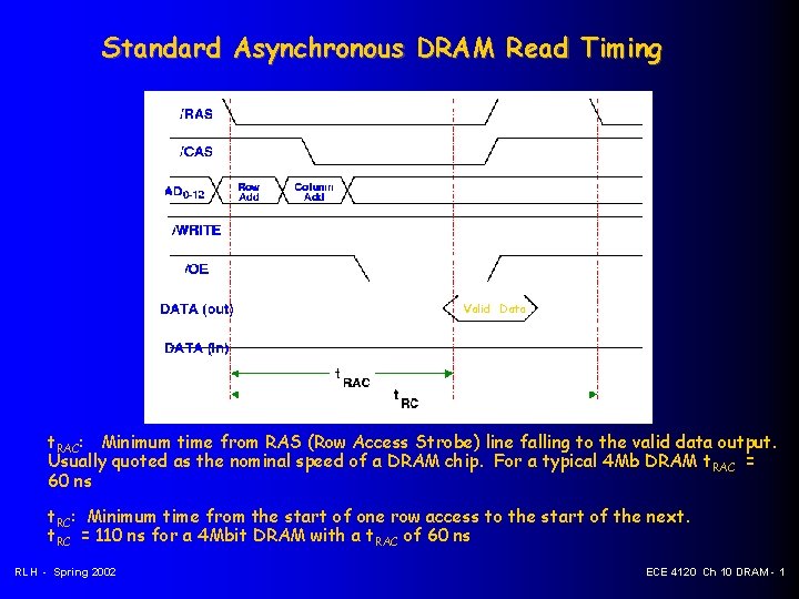
Key DRAM Timing Parameters t. RAC: minimum time from RAS line falling to the valid data output. – Quoted as the speed of a DRAM – A fast 4 Mb DRAM t. RAC = 60 ns t. RC: minimum time from the start of one row access to the start of the next. – t. RC = 110 ns for a 4 Mbit DRAM with a t. RAC of 60 ns t. CAC: minimum time from CAS line falling to valid data output. – 15 ns for a 4 Mbit DRAM with a t. RAC of 60 ns t. PC: minimum time from the start of one column access to the start of the next. – 35 ns for a 4 Mbit DRAM with a t. RAC of 60 ns RLH - Spring 2002 ECE 4120 Ch 10 DRAM - 1

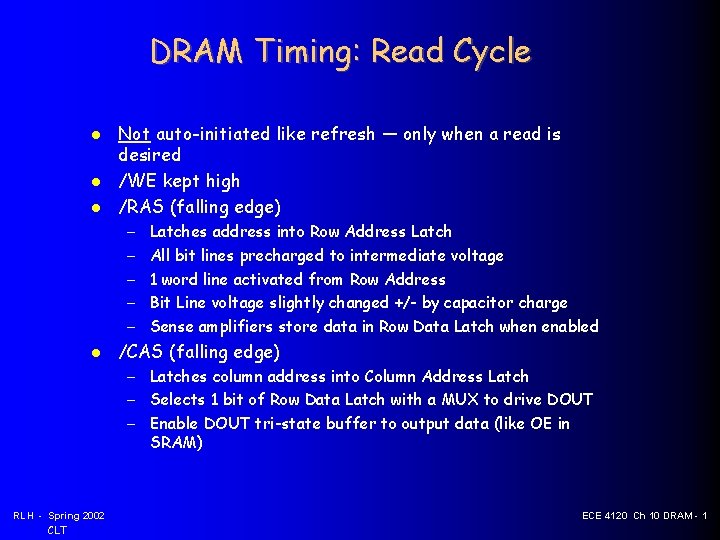
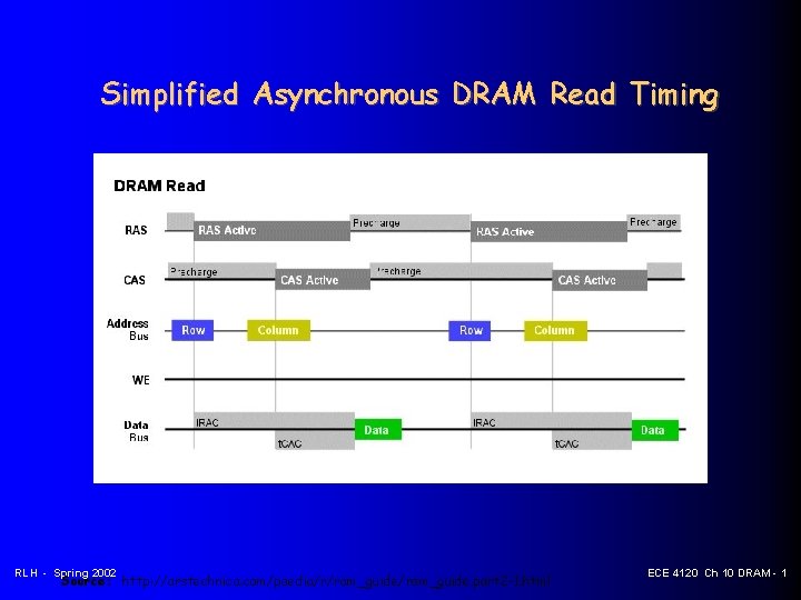
DRAM Timing: Read Cycle Not auto-initiated like refresh — only when a read is desired /WE kept high /RAS (falling edge) – – – Latches address into Row Address Latch All bit lines precharged to intermediate voltage 1 word line activated from Row Address Bit Line voltage slightly changed +/- by capacitor charge Sense amplifiers store data in Row Data Latch when enabled /CAS (falling edge) – Latches column address into Column Address Latch – Selects 1 bit of Row Data Latch with a MUX to drive DOUT – Enable DOUT tri-state buffer to output data (like OE in SRAM) RLH - Spring 2002 CLT ECE 4120 Ch 10 DRAM - 1

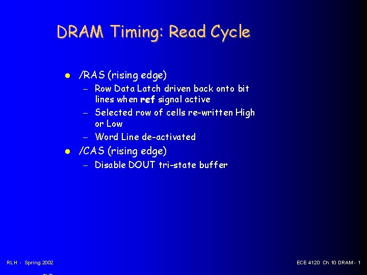
DRAM Timing: Read Cycle /RAS (rising edge) – Row Data Latch driven back onto bit lines when ref signal active – Selected row of cells re-written High or Low – Word Line de-activated /CAS (rising edge) – Disable DOUT tri-state buffer RLH - Spring 2002 ECE 4120 Ch 10 DRAM - 1

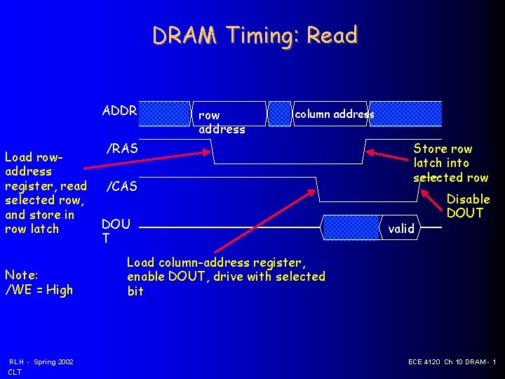
DRAM Timing: Read ADDR Load rowaddress register, read selected row, and store in row latch Note: /WE = High RLH - Spring 2002 CLT row address column address /RAS /CAS DOU T Store row latch into selected row valid Disable DOUT Load column-address register, enable DOUT, drive with selected bit ECE 4120 Ch 10 DRAM - 1

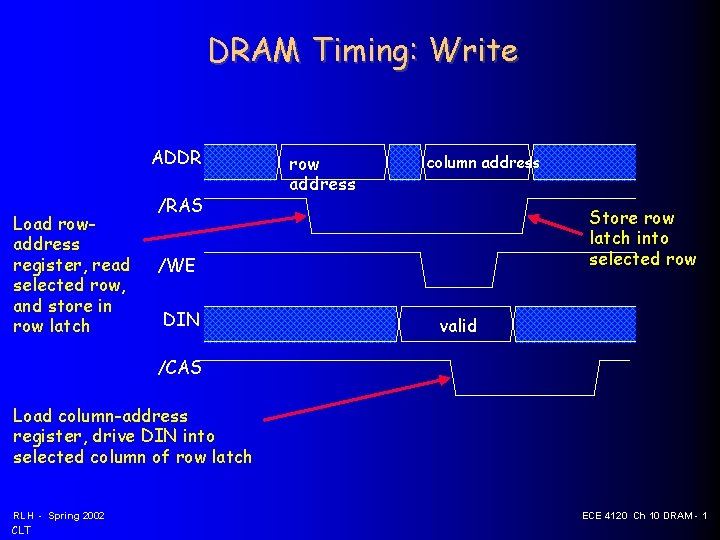
DRAM Timing: Write ADDR Load rowaddress register, read selected row, and store in row latch /RAS row address column address Store row latch into selected row /WE DIN valid /CAS Load column-address register, drive DIN into selected column of row latch RLH - Spring 2002 CLT ECE 4120 Ch 10 DRAM - 1

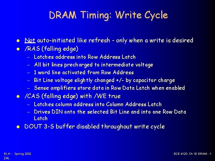
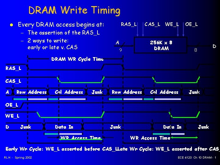
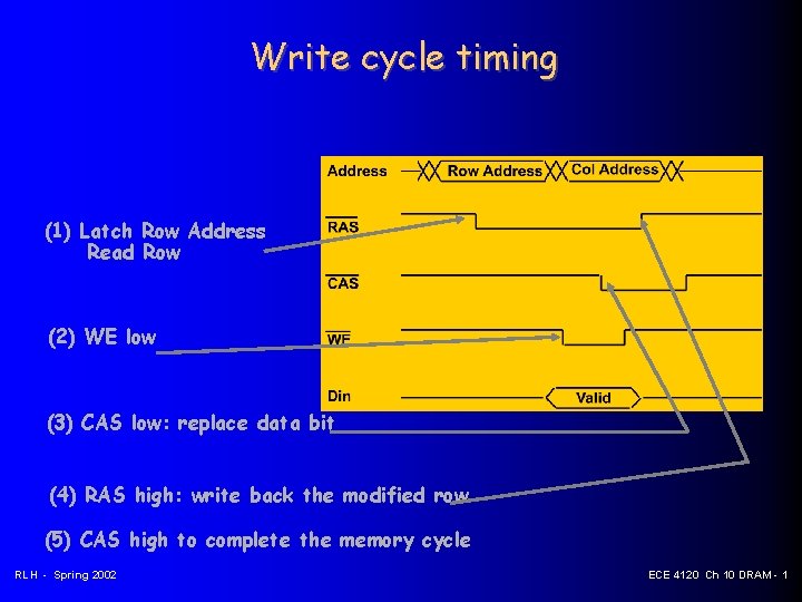
DRAM Timing: Write Cycle Not auto-initiated like refresh - only when a write is desired /RAS (falling edge) – – – Latches address into Row Address Latch All bit lines precharged to intermediate voltage 1 word line activated from Row Address Bit Line voltage slightly changed +/- by capacitor charge Sense amplifiers store data in Row Data Latch when enabled /CAS (falling edge) with /WE true – Latches column address into Column Address Latch – Drives DIN onto the selected Bit Line and into one Row Data Latch DOUT 3 -S buffer disabled throughout write cycle RLH - Spring 2002 JAL ECE 4120 Ch 10 DRAM - 1

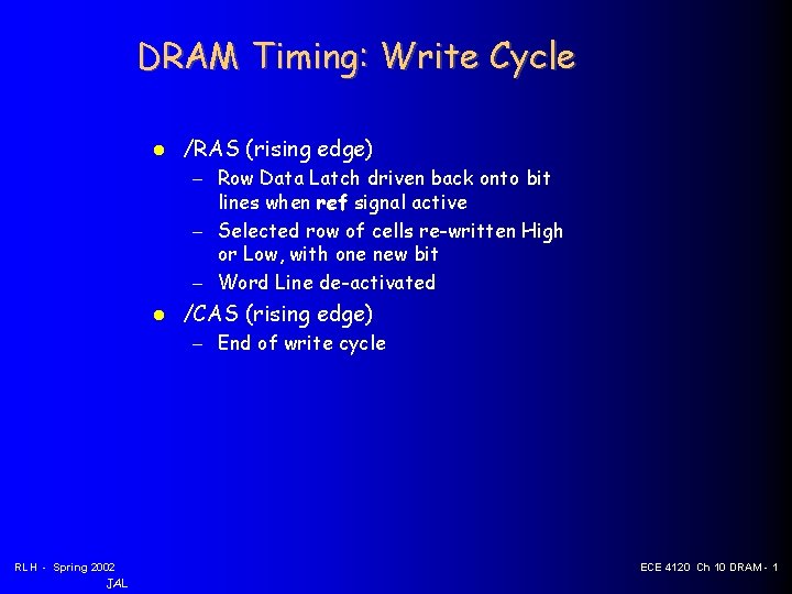
DRAM Timing: Write Cycle /RAS (rising edge) – Row Data Latch driven back onto bit lines when ref signal active – Selected row of cells re-written High or Low, with one new bit – Word Line de-activated /CAS (rising edge) – End of write cycle RLH - Spring 2002 JAL ECE 4120 Ch 10 DRAM - 1

DRAM Performance A 60 ns (t. RAC) DRAM can – perform a row access only every 110 ns (t. RC) – perform column access (t. CAC) in 15 ns, but time between column accesses is at least 35 ns (t. PC). In practice, external address delays and turning around buses make it 40 to 50 ns These times do not include the time to drive the addresses off the microprocessor nor the memory controller overhead. – Drive parallel DRAMs, external memory controller, bus to turn around, SIMM module, pins… – 180 ns to 250 ns latency from processor to memory is good for a “ 60 ns” (t. RAC) DRAM RLH - Spring 2002 ECE 4120 Ch 10 DRAM - 1

Standard Asynchronous DRAM Read Timing Valid Data t. RAC: Minimum time from RAS (Row Access Strobe) line falling to the valid data output. Usually quoted as the nominal speed of a DRAM chip. For a typical 4 Mb DRAM t. RAC = 60 ns t. RC: Minimum time from the start of one row access to the start of the next. t. RC = 110 ns for a 4 Mbit DRAM with a t. RAC of 60 ns RLH - Spring 2002 ECE 4120 Ch 10 DRAM - 1

Simplified Asynchronous DRAM Read Timing RLH - Spring 2002 Source: http: //arstechnica. com/paedia/r/ram_guide. part 2 -1. html ECE 4120 Ch 10 DRAM - 1

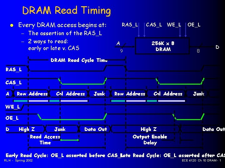
DRAM Read Timing Every DRAM access begins at: – The assertion of the RAS_L – 2 ways to read: early or late v. CAS RAS_L A CAS_L WE_L OE_L 256 K x 8 DRAM 9 D 8 DRAM Read Cycle Time RAS_L CAS_L A Row Address Col Address Junk WE_L OE_L D High Z Junk Read Access Time Data Out High Z Output Enable Delay Data Out Early Read Cycle: OE_L asserted before CAS_L Late Read Cycle: OE_L asserted after CAS RLH - Spring 2002 ECE 4120 Ch 10 DRAM - 1

DRAM Write Timing Every DRAM access begins at: – The assertion of the RAS_L – 2 ways to write: early or late v. CAS RAS_L A CAS_L WE_L 256 K x 8 DRAM 9 OE_L D 8 DRAM WR Cycle Time RAS_L CAS_L A Row Address Col Address Junk OE_L WE_L D Junk Data In WR Access Time Junk Data In Junk WR Access Time Early Wr Cycle: WE_L asserted before CAS_LLate Wr Cycle: WE_L asserted after CAS_ RLH - Spring 2002 ECE 4120 Ch 10 DRAM - 1

Write cycle timing (1) Latch Row Address Read Row (2) WE low (3) CAS low: replace data bit (4) RAS high: write back the modified row (5) CAS high to complete the memory cycle RLH - Spring 2002 ECE 4120 Ch 10 DRAM - 1

DRAM Read Timing Every DRAM access begins at: – The assertion of the RAS_L – 2 ways to read: early or late v. CAS RAS_L A CAS_L WE_L OE_L 256 K x 8 DRAM 9 D 8 DRAM Read Cycle Time RAS_L CAS_L A Row Address Col Address Junk WE_L OE_L D High Z Junk Read Access Time Data Out High Z Output Enable Delay Data Out Early Read Cycle: OE_L asserted before CAS_L Late Read Cycle: OE_L asserted after CAS RLH - Spring 2002 ECE 4120 Ch 10 DRAM - 1

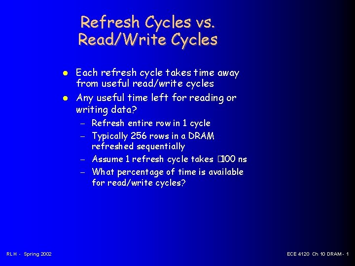
Refresh Cycles vs. Read/Write Cycles Each refresh cycle takes time away from useful read/write cycles Any useful time left for reading or writing data? – Refresh entire row in 1 cycle – Typically 256 rows in a DRAM refreshed sequentially – Assume 1 refresh cycle takes � 100 ns – What percentage of time is available for read/write cycles? RLH - Spring 2002 ECE 4120 Ch 10 DRAM - 1

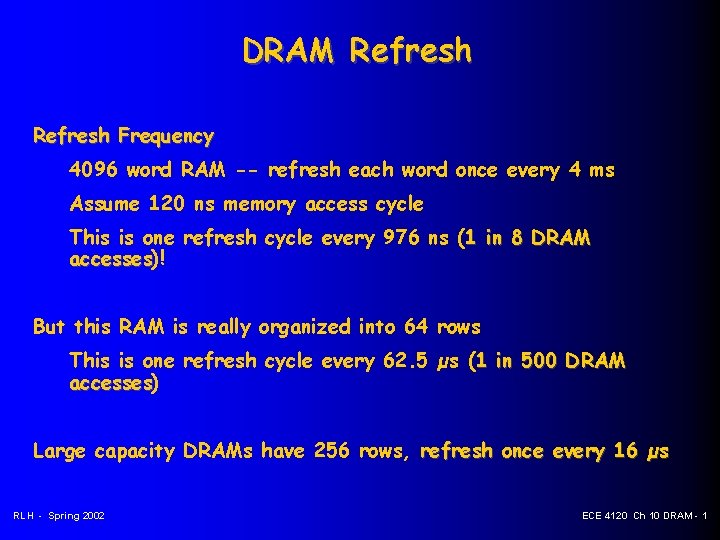
DRAM Refresh Frequency 4096 word RAM -- refresh each word once every 4 ms Assume 120 ns memory access cycle This is one refresh cycle every 976 ns (1 in 8 DRAM accesses)! accesses But this RAM is really organized into 64 rows This is one refresh cycle every 62. 5 µs (1 in 500 DRAM accesses) accesses Large capacity DRAMs have 256 rows, refresh once every 16 µs RLH - Spring 2002 ECE 4120 Ch 10 DRAM - 1

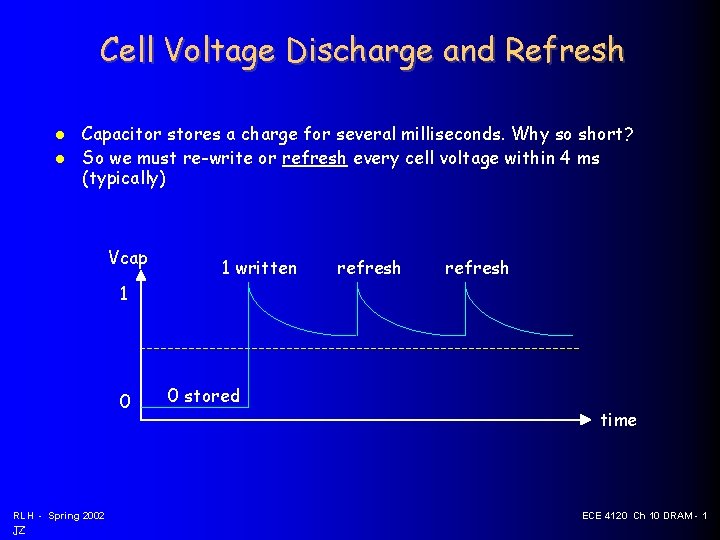
Cell Voltage Discharge and Refresh Capacitor stores a charge for several milliseconds. Why so short? So we must re-write or refresh every cell voltage within 4 ms (typically) Vcap 1 written refresh 1 0 RLH - Spring 2002 JZ 0 stored time ECE 4120 Ch 10 DRAM - 1

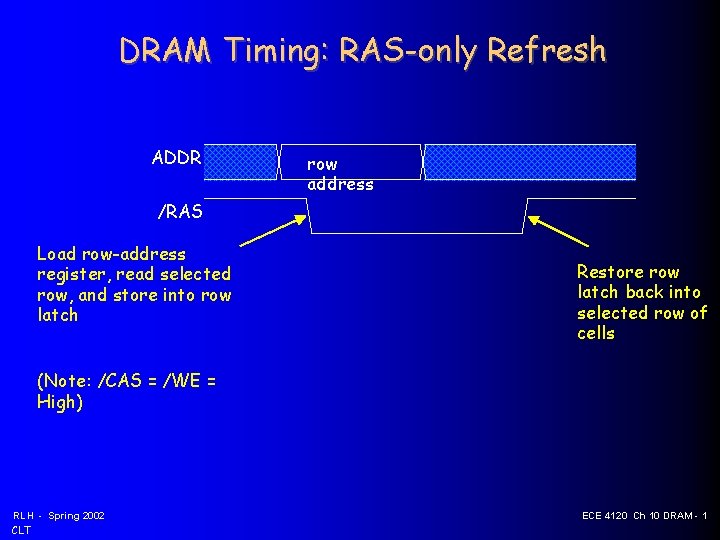
DRAM Timing: RAS-only Refresh ADDR row address /RAS Load row-address register, read selected row, and store into row latch Restore row latch back into selected row of cells (Note: /CAS = /WE = High) RLH - Spring 2002 CLT ECE 4120 Ch 10 DRAM - 1

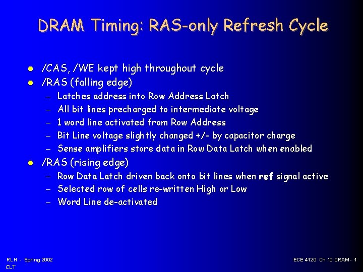
DRAM Timing: RAS-only Refresh Cycle /CAS, /WE kept high throughout cycle /RAS (falling edge) – – – Latches address into Row Address Latch All bit lines precharged to intermediate voltage 1 word line activated from Row Address Bit Line voltage slightly changed +/- by capacitor charge Sense amplifiers store data in Row Data Latch when enabled /RAS (rising edge) – Row Data Latch driven back onto bit lines when ref signal active – Selected row of cells re-written High or Low – Word Line de-activated RLH - Spring 2002 CLT ECE 4120 Ch 10 DRAM - 1

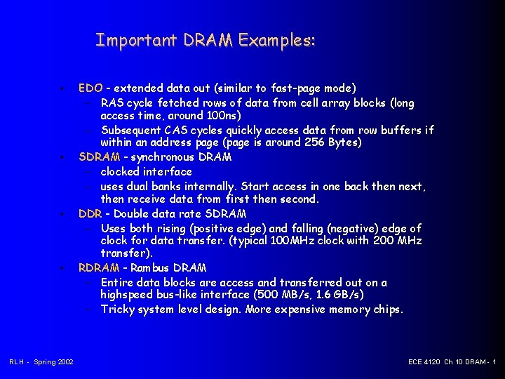
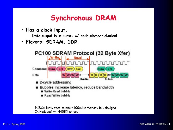
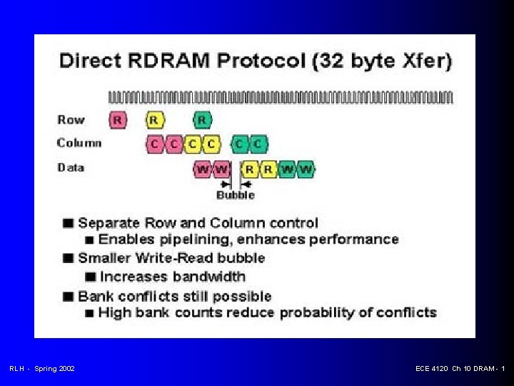
Important DRAM Examples: • • RLH - Spring 2002 EDO - extended data out (similar to fast-page mode) – RAS cycle fetched rows of data from cell array blocks (long access time, around 100 ns) – Subsequent CAS cycles quickly access data from row buffers if within an address page (page is around 256 Bytes) SDRAM - synchronous DRAM – clocked interface – uses dual banks internally. Start access in one back then next, then receive data from first then second. DDR - Double data rate SDRAM – Uses both rising (positive edge) and falling (negative) edge of clock for data transfer. (typical 100 MHz clock with 200 MHz transfer). RDRAM - Rambus DRAM – Entire data blocks are access and transferred out on a highspeed bus-like interface (500 MB/s, 1. 6 GB/s) – Tricky system level design. More expensive memory chips. ECE 4120 Ch 10 DRAM - 1

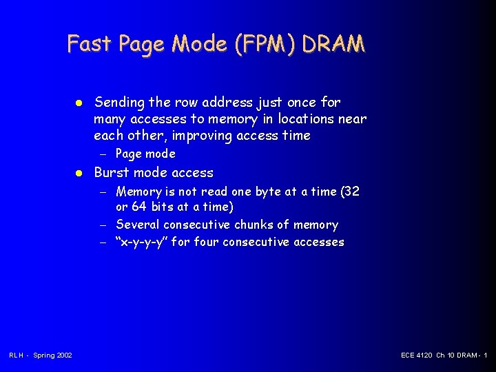
Fast Page Mode (FPM) DRAM Sending the row address just once for many accesses to memory in locations near each other, improving access time – Page mode Burst mode access – Memory is not read one byte at a time (32 or 64 bits at a time) – Several consecutive chunks of memory – “x-y-y-y” for four consecutive accesses RLH - Spring 2002 ECE 4120 Ch 10 DRAM - 1

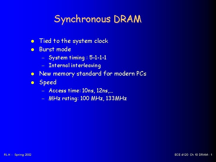
Synchronous DRAM Tied to the system clock Burst mode – System timing : 5 -1 -1 -1 – Internal interleaving New memory standard for modern PCs Speed – Access time: 10 ns, 12 ns, … – MHz rating: 100 MHz, 133 MHz RLH - Spring 2002 ECE 4120 Ch 10 DRAM - 1

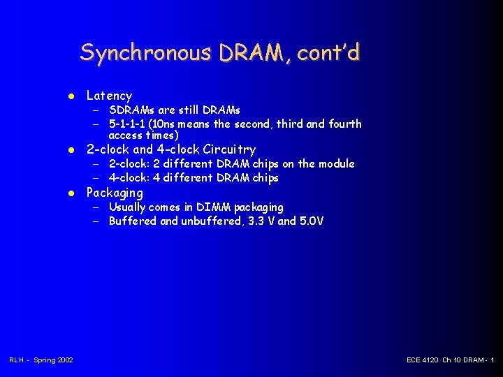
Synchronous DRAM, cont’d Latency 2 -clock and 4 -clock Circuitry Packaging RLH - Spring 2002 – SDRAMs are still DRAMs – 5 -1 -1 -1 (10 ns means the second, third and fourth access times) – 2 -clock: 2 different DRAM chips on the module – 4 -clock: 4 different DRAM chips – Usually comes in DIMM packaging – Buffered and unbuffered, 3. 3 V and 5. 0 V ECE 4120 Ch 10 DRAM - 1

RLH - Spring 2002 ECE 4120 Ch 10 DRAM - 1

RDRAM RLH - Spring 2002 ECE 4120 Ch 10 DRAM - 1

RLH - Spring 2002 ECE 4120 Ch 10 DRAM - 1

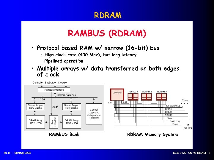
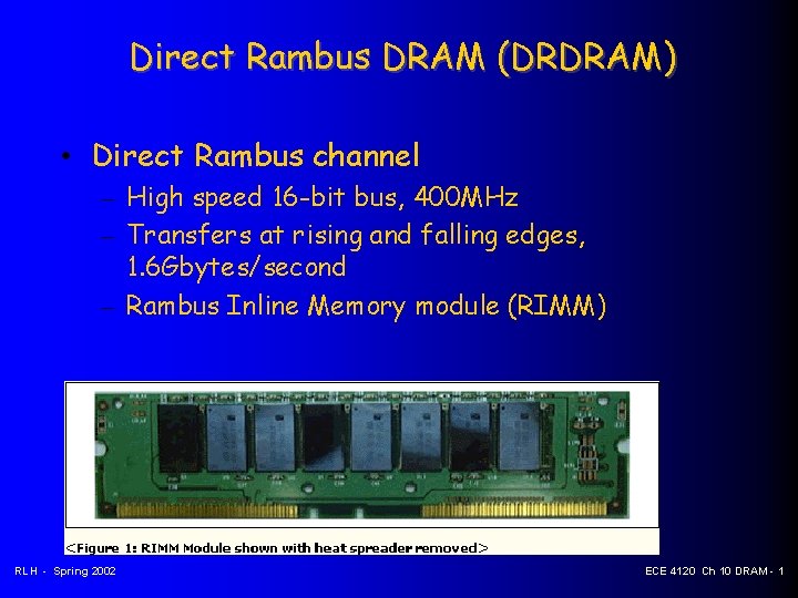
Direct Rambus DRAM (DRDRAM) • Direct Rambus channel – High speed 16 -bit bus, 400 MHz – Transfers at rising and falling edges, 1. 6 Gbytes/second – Rambus Inline Memory module (RIMM) RLH - Spring 2002 ECE 4120 Ch 10 DRAM - 1

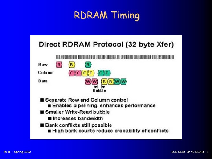
RDRAM Timing RLH - Spring 2002 ECE 4120 Ch 10 DRAM - 1

Synchronous-Link DRAM (SLDRAM) SLDRAM Consortium – Evolutionary design – 64 bit bus running at a 200 MHz clock speed (effective speed of 400 MHz) – 3. 2 Gbytes/second – Open standard RLH - Spring 2002 ECE 4120 Ch 10 DRAM - 1

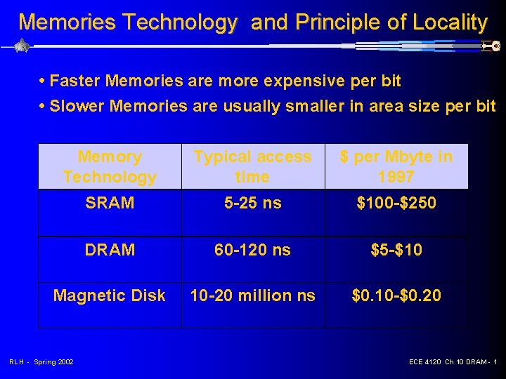
Memories Technology and Principle of Locality • Faster Memories are more expensive per bit • Slower Memories are usually smaller in area size per bit Memory Technology Typical access time $ per Mbyte in 1997 SRAM 5 -25 ns $100 -$250 DRAM 60 -120 ns $5 -$10 Magnetic Disk 10 -20 million ns $0. 10 -$0. 20 RLH - Spring 2002 ECE 4120 Ch 10 DRAM - 1

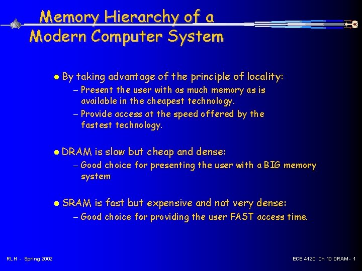
Memory Hierarchy of a Modern Computer System By taking advantage of the principle of locality: – Present the user with as much memory as is available in the cheapest technology. – Provide access at the speed offered by the fastest technology. DRAM is slow but cheap and dense: – Good choice for presenting the user with a BIG memory system SRAM is fast but expensive and not very dense: – Good choice for providing the user FAST access time. RLH - Spring 2002 ECE 4120 Ch 10 DRAM - 1