Trends in DRAM 2021619 4 DRAM ProcessorDRAM Memory


 Processor-Memory Performance Gap Growing 2021/6/19 计算机体系结构 5")


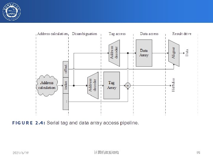
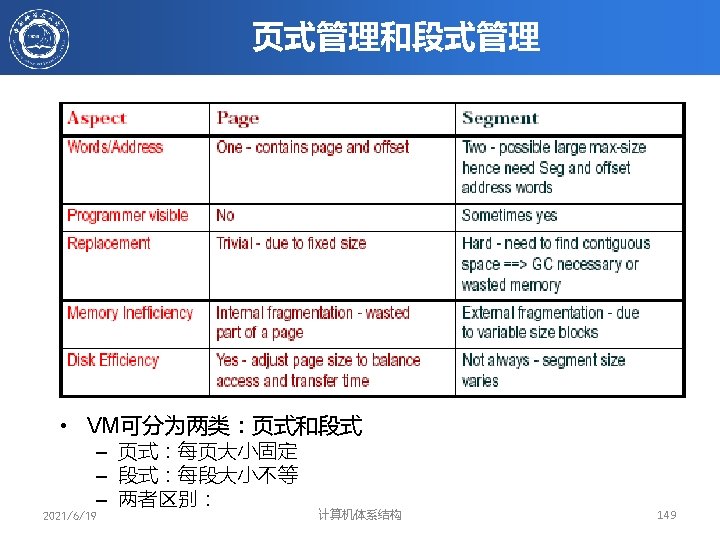
 • 假设采用二级存储:M 1和M 2 – M 1和M 2的容量、价格、访问时间分别为: – S 1 、C 1、TA")

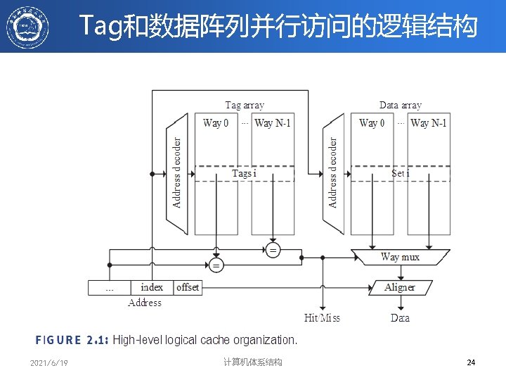
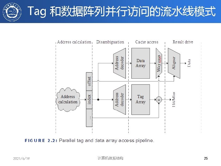
: 查找方法 • 在CACHE中每一block都带有tag域(标记域), 标记分为两类 – Address Tags:标记所访问的单元在哪一块中,这样 物理地址就分为三部分: Address Tags ## Block")


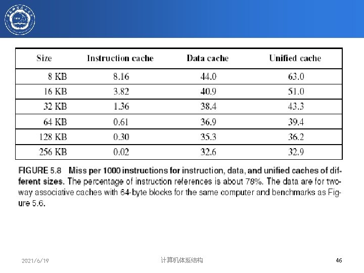
 Data Cache misses per 1000 instructions comparing LRU, Random, FIFO replacement for several")


 2021/6/19 计算机体系结构 39")


 Proc Unified Cache-1 I-Cache-1 D-Cache-1")


 • 在Cache和Memory之间增加一个小的全相联Cache 2021/6/19 计算机体系结构 63")


 – 在现代处理器中保持较高的指令吞吐率 • True Multi-ported")


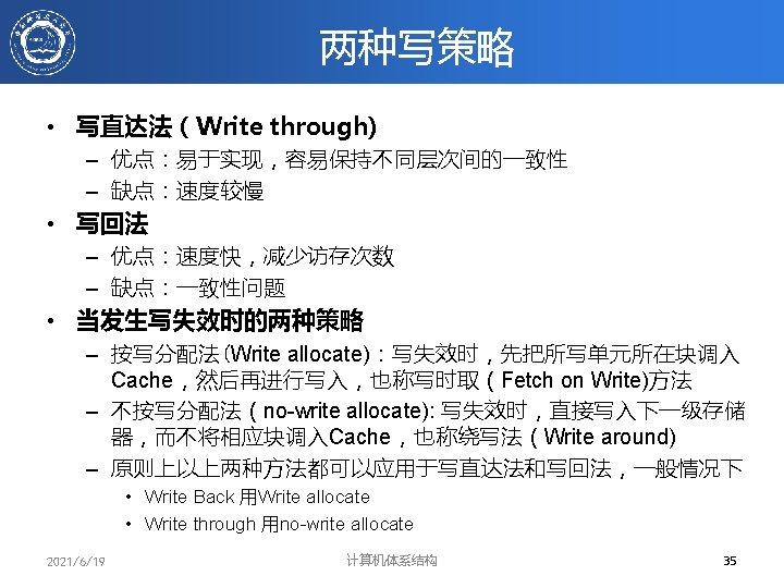
![编译器优化方法举例之一:数组合并 // Original Code for (i = 0; i < N; i++) a[i] =](https://slidetodoc.com/presentation_image_h2/8010268200318c4ddcdb330a00cabc71/image-108.jpg "编译器优化方法举例之一:数组合并 // Original Code for (i = 0; i < N; i++) a[i] =")
 /* After */ for (jj = 0; jj < N; jj =")
 Pentium 4 Pre-fetching 2021/6/19")


![for (j = 0; j < 100; j = j+1) { prefetch(b[j+7][0]); /* b(j,](https://slidetodoc.com/presentation_image_h2/8010268200318c4ddcdb330a00cabc71/image-118.jpg "for (j = 0; j < 100; j = j+1) { prefetch(b[j+7][0]); /* b(j,")
 Ignore instruction")


 Clock and control signals ~7 Address lines multiplexed row/column address ~12")


,Higher")
")


. Modern dram architectures,")


")
 Extended-data-out (EDO) Burst-EDO (BEDO) Synchronous DRAM (SDRAM)")
")


- Slides: 165
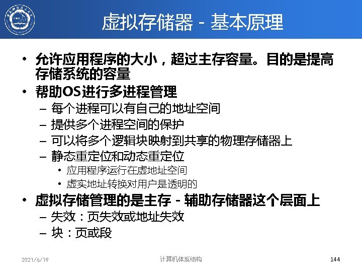
Trends in DRAM 2021/6/19 计算机体系结构 4
微处理器与DRAM 的性能差异 Processor-DRAM Memory Gap (latency) Processor-Memory Performance Gap Growing 2021/6/19 计算机体系结构 5
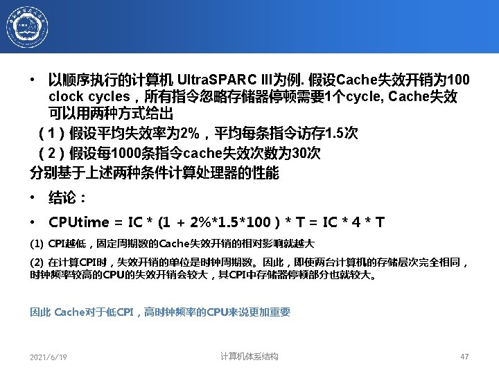
Microprocessor-DRAM性能差异 • 利用caches缓解微处理器与存储器性能上的差异 • Microprocessor-DRAM 性能差异 – – 2021/6/19 time of a full cache miss in instructions executed 1 st Alpha : 340 ns/5. 0 ns = 68 clks x 2 or 136 instructions 2 nd Alpha : 266 ns/3. 3 ns = 80 clks x 4 or 320 instructions 3 rd Alpha : 180 ns/1. 7 ns =108 clks x 6 or 648 instructions 计算机体系结构 6
存储系统的设计目标 Workload or Benchmark programs Processor reference stream <op, addr>, . . . op: i-fetch, read, write Memory $ 通过优化存储系统的组织来使得针对典型应 用平均访存时间最短 MEM 2021/6/19 计算机体系结构 7
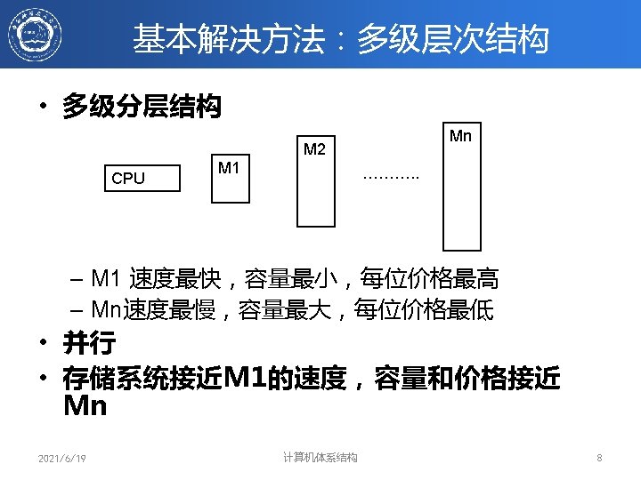
计算机系统的多级存储层次 CPU Register L 1 L 2 L 3 C A C H E I/O device MEMORY Server 300 ps 1 ns 3 -10 ns 10 -20 ns 50 -100 ns 5 -10 ms 1000 B 64 KB 256 K 2 -4 MB 4 -16 GB 4 -16 TB L 1 L 2 C A C H E 500 ps 2 ns 1020 ns 500 B 64 KB 256 K 计算机体系结构 256 -512 MB CPU Register MEMORY I/O device PMD 2021/6/19 50 -100 ns 25 -50μs 4 -8 GB 9
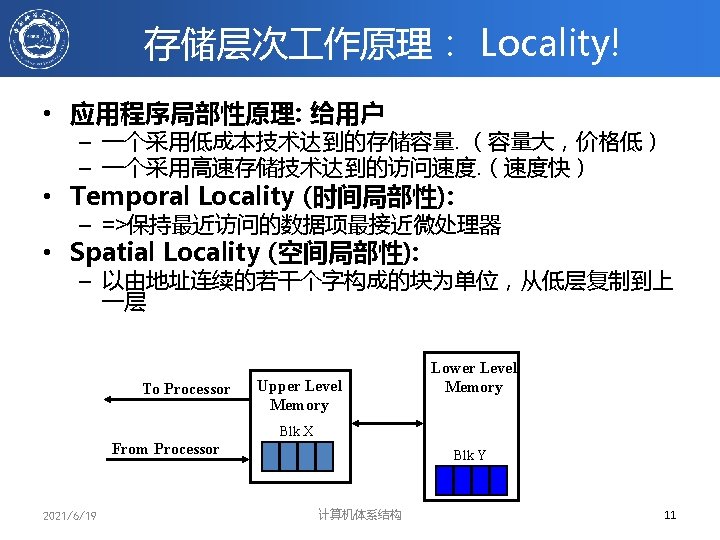
存储层次的性能参数(1/2) • 假设采用二级存储:M 1和M 2 – M 1和M 2的容量、价格、访问时间分别为: – S 1 、C 1、TA 1 S 2、C 2、TA 2 To Processor Upper Level Memory Lower Level Memory Blk X From Processor 2021/6/19 Blk Y 计算机体系结构 13
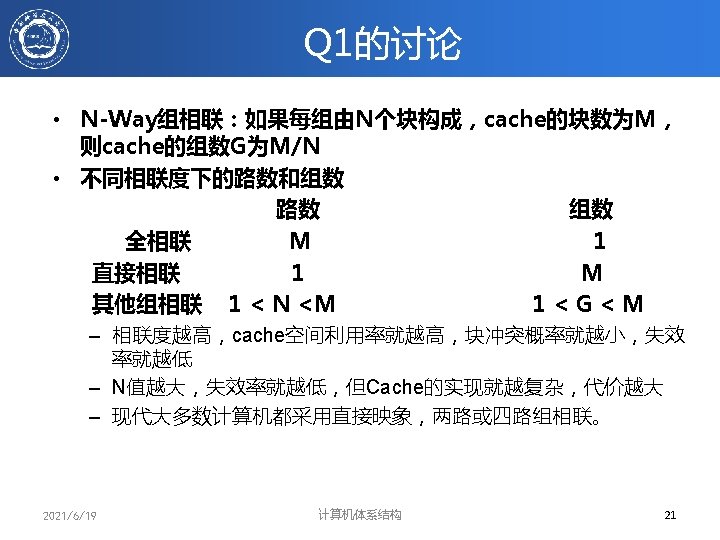
Q 1: Where can a block be placed in the upper level? • Block 12 placed in 8 block cache: – – Fully associative, direct mapped, 2 -way set associative S. A. Mapping = Block Number Modulo Number Sets Fully associative: block 12 can go anywhere Block no. 01234567 Direct mapped: block 12 can go only into block 4 (12 mod 8) Block no. 01234567 Set associative: block 12 can go anywhere in set 0 (12 mod 4) Block no. Set Set 0 1 2 3 Block-frame address Block no. 2021/6/19 01234567 111112222233 0123456789012345678901 计算机体系结构 20
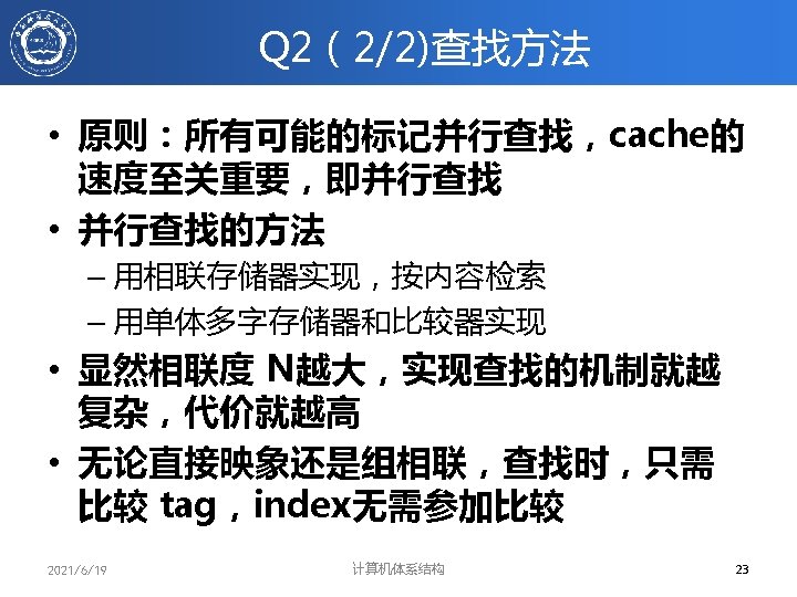
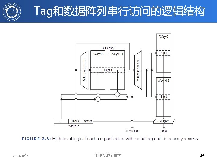
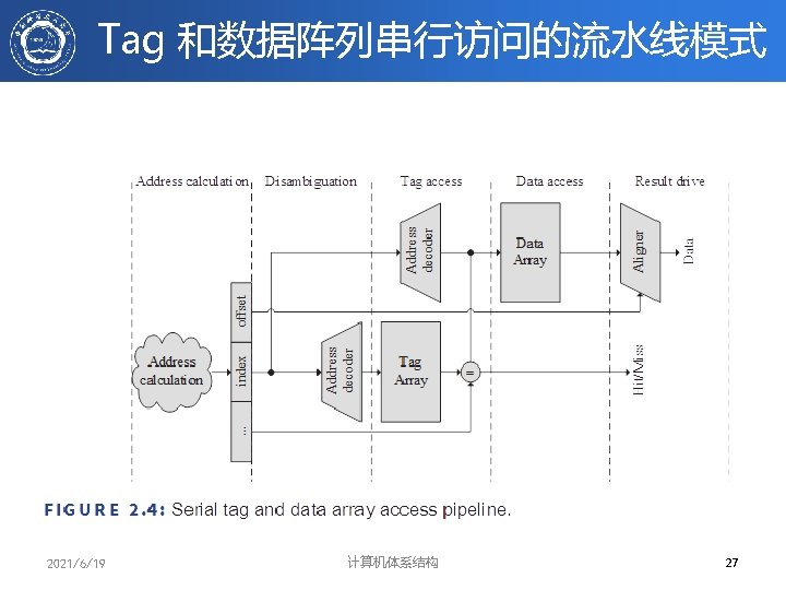
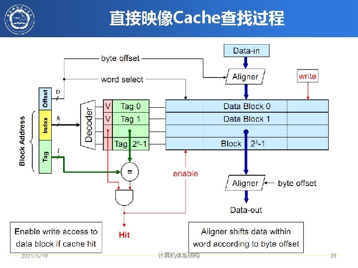
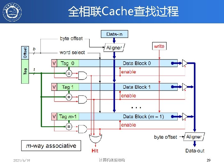
Q 2(1/2): 查找方法 • 在CACHE中每一block都带有tag域(标记域), 标记分为两类 – Address Tags:标记所访问的单元在哪一块中,这样 物理地址就分为三部分: Address Tags ## Block index## block Offset – 全相联映象时,没有Block Index – 显然 Address tag越短,查找所需代价就越小 – Status Tags:标记该块的状态,如Valid, Dirty等 Block Address Block offset Index Tag Set Select 2021/6/19 计算机体系结构 Data Select 22
Example: 1 KB Direct Mapped Cache with 32 B Blocks • 对于容量为 2 N 字节的cache: – 最高(32 -N)位部分 为 Cache Tag – 最低M位为字节选择位 (Block Size = 2 M) Block address Cache Tag Example: 0 x 50 Stored as part of the cache “state” Cache Tag Cache Data Byte 31 Byte 63 : : Valid Bit 0 x 50 : 9 Cache Index Ex: 0 x 01 Byte 0 0 Byte 33 Byte 32 1 2 3 : : Byte 1023 2021/6/19 4 0 Byte Select Ex: 0 x 00 计算机体系结构 : 31 Byte 992 31 30
Example: Set Associative Cache • N-way set associative: 每一个cache索引对应N个cache entries – 这N个cache项并行操作 • Example: Two-way set associative cache – Cache index 选择cache中的一组 – 这一组中的两块对应的Tags与输入的地址同时比较 – 根据比较结果选择数据 Valid Cache Tag : : Adr Tag Compare Cache Index Cache Data Cache Block 1 Cache Block 0 : : Sel 1 1 Mux 0 Sel 0 Cache Tag Valid : : Compare OR Hit 2021/6/19 Cache Block 计算机体系结构 31
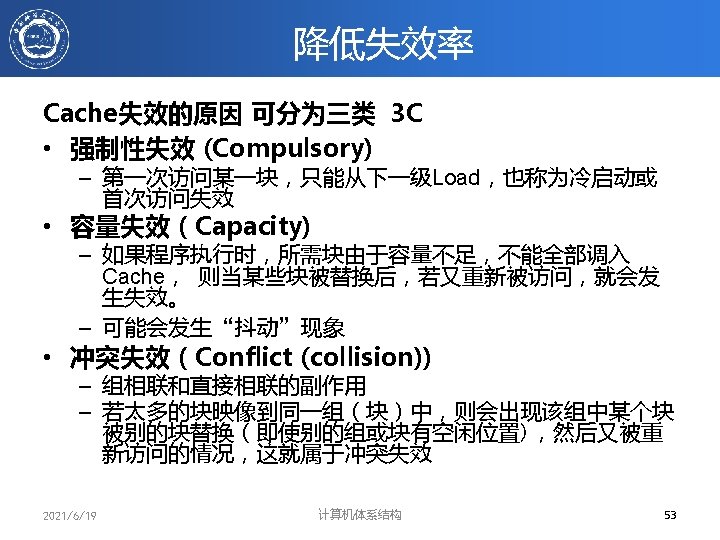
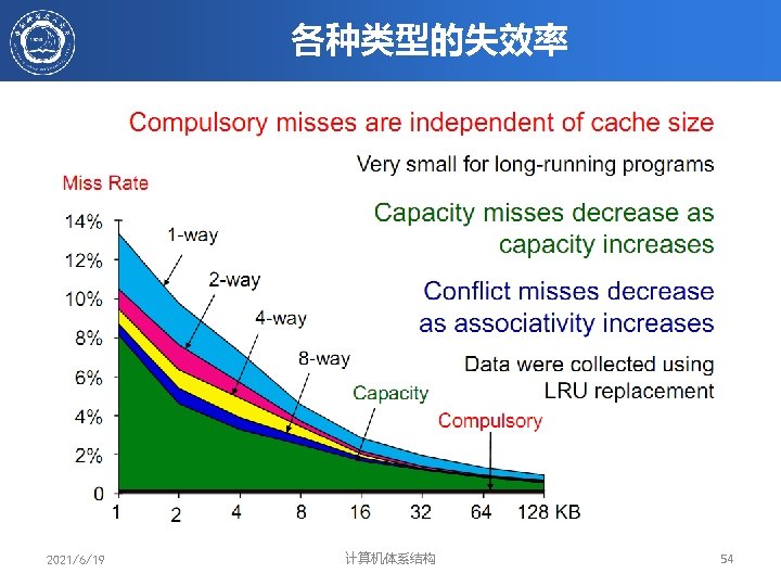
LRU和Random的比较(失效率) Data Cache misses per 1000 instructions comparing LRU, Random, FIFO replacement for several sizes and associativities. These data were collected for a block size of 64 bytes for the Alpha architecture using 10 SPEC 2000 benchmarks. Five are from SPECint 2000(gap, gcc, gzip, mcf and perl) and five are from SPECfp 2000(applu, art, equake, lucas and swim) • 观察结果(失效率) – – 2021/6/19 相联度高,失效率较低。 Cache容量较大,失效率较低。 LRU 在Cache容量较小时,失效率较低 随着Cache容量的加大,Random的失效率在降低 计算机体系结构 33
Write-back, Write Allocate 2021/6/19 计算机体系结构 36
Write-Through, No Write Allocate 2021/6/19 计算机体系结构 37
Alpha AX 21064 Cache结构(数据Cache) 2021/6/19 计算机体系结构 39
Alpha 21264 Data Cache • 基本技术特征 – Cache size: 64 Kbytes – Block size: 64 -bytes – Two-way 组相联 – Write back, 写失效时,write allocate • 21264 48 -bits 虚拟地址,虚实映射为 44 bits的物理地址,也支持43 -bits虚拟地址, 虚实映射为 41 -bits的物理地址 – 29位tags##9位index##6位 Block offset 2021/6/19 计算机体系结构 40
Alpha 21264 Data Cache 2021/6/19 计算机体系结构 41
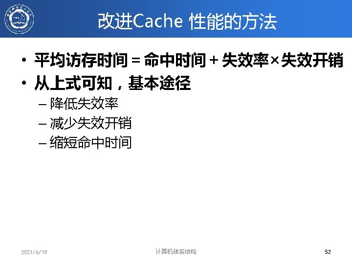
Cache 性能分析 • CPU time = (CPU execution clock cycles + Memory stall clock cycles) x clock cycle time • Memory stall clock cycles = (Reads x Read miss rate x Read miss penalty + Writes x Write miss rate x Write miss penalty) • Memory stall clock cycles = Memory accesses x Miss rate x Miss penalty • Different measure: AMAT Average Memory Access time (AMAT) = Hit Time + (Miss Rate x Miss Penalty) • Note: memory hit time is included in execution cycles. 2021/6/19 计算机体系结构 43
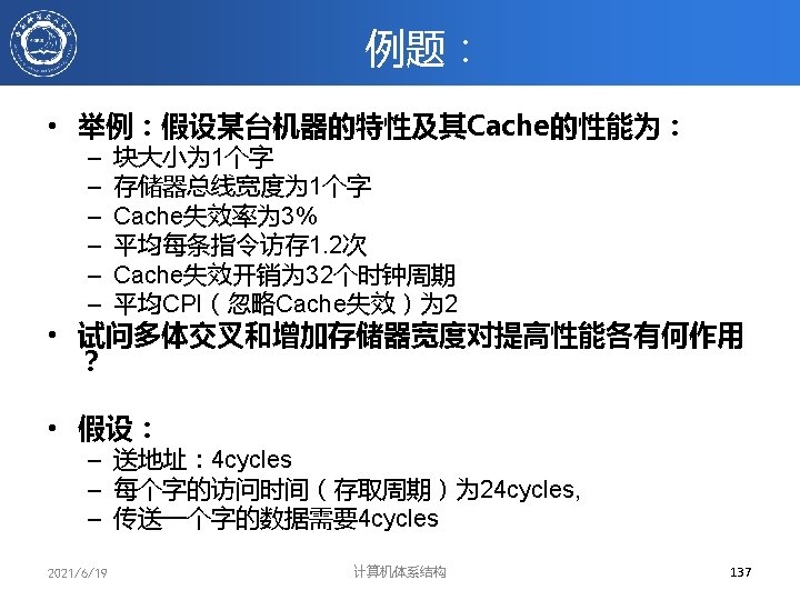
性能分析举例 § Suppose a processor executes at • Clock Rate = 200 MHz (5 ns per cycle), Ideal (no misses) CPI = 1. 1 • 50% arith/logic, 30% ld/st, 20% control § Miss Behavior: • 10% of memory operations get 50 cycle miss penalty • 1% of instructions get same miss penalty § CPI = ideal CPI + average stalls per instruction = 1. 1(cycles/ins) + [ 0. 30 (Data. Mops/ins) x 0. 10 (miss/Data. Mop) x 50 (cycle/miss)] + [ 1 (Inst. Mop/ins) x 0. 01 (miss/Inst. Mop) x 50 (cycle/miss)] = (1. 1 + 1. 5 +. 5) cycle/ins = 3. 1 § 65% (2/3. 1) of the time the proc is stalled waiting for memory! § AMAT=(1/1. 3)x[1+0. 01 x 50]+(0. 3/1. 3)x[1+0. 1 x 50]=2. 54 2021/6/19 计算机体系结构 44
Example: Harvard Architecture • Unified vs Separate I&D (Harvard) Proc Unified Cache-1 I-Cache-1 D-Cache-1 Unified Cache-2 • Proc Statistics (given in H&P): – 16 KB I&D: Inst miss rate=0. 64%, Data miss rate=6. 47% – 32 KB unified: Aggregate miss rate=1. 99% • • • Which is better (ignore L 2 cache)? – Assume 33% data ops 75% accesses from instructions (1. 0/1. 33) – hit time=1, miss time=50 – Note that data hit has 1 stall for unified cache (only one port) AMATHarvard=75%x(1+0. 64%x 50)+25%x(1+6. 47%x 50) = 2. 05 AMATUnified =75%x(1+1. 99%x 50)+25%x(1+1+1. 99%x 50)= 2. 24 2021/6/19 计算机体系结构 45
Summary of performance equations in this chapter 2021/6/19 计算机体系结构 50
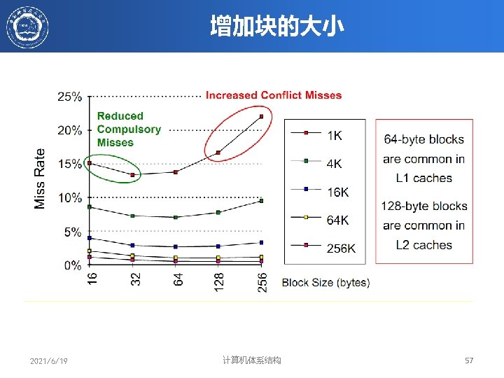
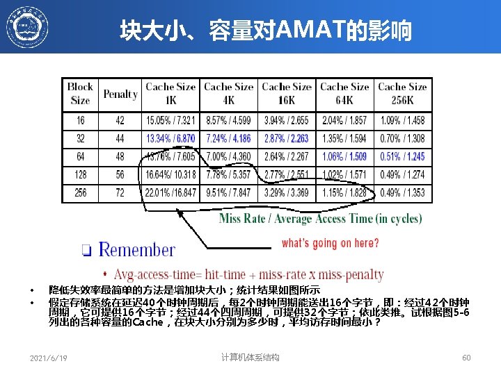
块大小、容量对失效率的影响 • Given: miss rates for different cache sizes & block sizes • Memory latency = 80 cycles + 1 cycle per 8 bytes ‒ Latency of 16 -byte block = 80 + 2 = 82 clock cycles ‒ Latency of 32 -byte block = 80 + 4 = 84 clock cycles ‒ Latency of 256 -byte block = 80 + 32 = 112 clock cycles • Which block has smallest AMAT for each cache size? 2021/6/19 计算机体系结构 58
块大小、容量对AMAT的影响 • Solution: assume hit time = 1 clock cycle – Regardless of block size and cache size • Cache Size = 4 KB, Block Size = 16 bytes – AMAT = 1 + 8. 57% × 82 = 8. 027 clock cycles • Cache Size = 256 KB, Block Size = 256 bytes – AMAT = 1 + 0. 49% × 112 = 1. 549 clock cycles 2021/6/19 计算机体系结构 59
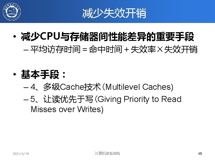
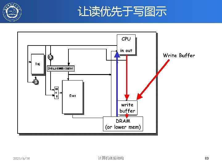
Victim Cache(1/2) • 在Cache和Memory之间增加一个小的全相联Cache 2021/6/19 计算机体系结构 63
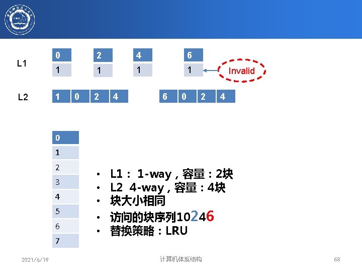
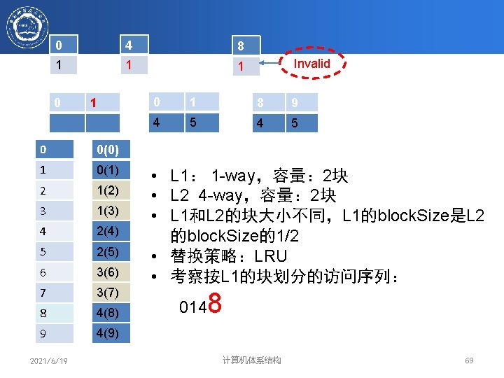
0 2 2 4 4 6 6 1 1 3 3 5 5 3 0 0 1 0 L 2 #3 L 1 #5互� Write Back 0 1 2 Set 0 0 1 4 1 2 3 4 1 2 5 0 • L 1: 1 -way L 2: 2 -way 1 2 • 访问的块序列 0123456 3 4 3 • 替换策略:LRU 5 • 块大小相同 6 2021/6/19 计算机体系结构 71
04/01 -review:Cache 性能分析 • CPU time = (CPU execution clock cycles + Memory stall clock cycles) x clock cycle time • Memory stall clock cycles = (Reads x Read miss rate x Read miss penalty + Writes x Write miss rate x Write miss penalty) • Memory stall clock cycles = Memory accesses x Miss rate x Miss penalty • Different measure: AMAT Average Memory Access time (AMAT) = Hit Time + (Miss Rate x Miss Penalty) • Note: memory hit time is included in execution cycles. 2021/6/19 计算机体系结构 72
多级cache的性能分析 • 局部失效率:该级Cache的失效次数 / 到达该级Cache的访存 次数 – Miss rate. L 1 for L 1 cache – Miss rate. L 2 for L 2 cache • 全局失效率:该级Cache的失效次数/ CPU发出的访存总次数 – Miss rate. L 1 for L 1 cache – Miss rate. L 1 × Miss rate. L 2 for L 2 cache – 全局失效率是度量L 2 cache性能的更好方法 • 性能参数 – AMAT = Hit Time. L 1+Miss rate. L 1×Miss penalty. L 1 – Miss penalty. L 1 = Hit. Time. L 2 + Miss rate. L 2×Miss penalty. L 2 – AMAT = Hit Time. L 1+Miss rate. L 1× (Hit Time. L 2+Miss rate. L 2×Miss penalty. L 2) 2021/6/19 计算机体系结构 74
L 1 cache 失效率 • 对于I-Cache和D-Cache分开的L 1 Cache Miss Rate. L 1 = %inst × Miss Rate. I-Cache + %data × Miss Rate. DCache %inst = Percent of Instruction Accesses = 1 / (1 + %LS) %data = Percent of Data Accesses = %LS / (1 + %LS) %LS = Frequency of Load and Store instructions • 每条指令的L 1 失效次数: Misses per Instruction. L 1 = Miss Rate. L 1 × (1 + %LS) Misses per Instruction. L 1 = Miss Rate. I-Cache + %LS × Miss Rate. D -Cache 2021/6/19 计算机体系结构 75
Memory Stall Cycles Per Instruction • Memory Stall Cycles per Instruction = Memory Access per Instruction × Miss Rate. L 1 × Miss Penalty. L 1 = (1 + %LS) × Miss Rate. L 1 × (Hit Time. L 2 + Miss Rate. L 2 × Miss Penalty. L 2) • Memory Stall Cycles per Instruction = Misses per Instruction. L 1 × Hit Time. L 2 + Misses per Instruction. L 2 × Miss Penalty. L 2 Misses per Instruction. L 1 = (1 + %LS) × Miss Rate. L 1 Misses per Instruction. L 2 = (1 + %LS) × Miss Rate. L 1 × Miss Rate. L 2 2021/6/19 计算机体系结构 77
两级Cache的性能 • Problem: 程序运行产生 1000个存储器访问 – I-Cache misses = 5, D-Cache misses = 35, L 2 Cache misses = 8 – L 1 Hit = 1 cycle, L 2 Hit = 8 cycles, L 2 Miss penalty = 80 cycles – Load + Store frequency = 25%, CPIexecution = 1. 1 (perfect cache) – 计算memory stall cycles per instruction 和有效的CPI – 如果没有L 2 cache, 有效的CPI是多少? • Solution: – – – L 1 Miss Rate = (5 + 35) / 1000 = 0. 04 (or 4% per access) L 1 misses per Instruction =0. 04 × (1 + 0. 25) = 0. 05 L 2 misses per Instruction =(8 / 1000) × 1. 25 = 0. 01 Memory stall cycles per Instruction =0. 05 × 8 + 0. 01 × 80 = 1. 2 CPIL 1+L 2 = 1. 1 + 1. 2 = 2. 3, CPI/CPIexecution = 2. 3/1. 1 = 2. 1 x slower – CPIL 1 only =1. 1 + 0. 05 × 80 = 5. 1 (worse) 2021/6/19 计算机体系结构 78
Miss rates versus cache size for multilevel caches 2021/6/19 计算机体系结构 80
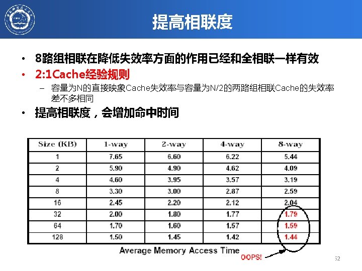
多级Cache举例 Given the data below, what is the impact of second-level cache associativity on its miss penalty? – Hit time. L 2 for direct mapped = 10 clock cycles – Two-way set associativity increases hit time by 0. 1 clock cycles to 10. 1 clock cycles – Local miss rate. L 2 for direct mapped = 25% – Local miss rate. L 2 for two-way set associative = 20% – Miss penalty. L 2 = 100 clock cycles • 结论:提高相联度,可减少第一级Cache的失效开销 • 第二级Cache特点:容量大,高相联度,块较大,重点 减少失效次数。 2021/6/19 计算机体系结构 82
缩短命中时间 虚拟地址Cache VS. 物理地址Cache Figure B. 16 Miss rate versus virtually addressed cache size of a program measured three ways: without process switches (uniprocess), with process switches using a process-identifier tag (PID), and with process switches but without PIDs (purge). PIDs increase the uniprocess absolute miss rate by 0. 3% to 0. 6% and save 0. 6% to 4. 3% over purging. Agarwal [1987] collected these statistics for the Ultrix operating system running on a VAX, assuming direct-mapped caches with a block size of 16 bytes. Note that the miss rate goes up from 128 K to 256 K. Such nonintuitive behavior can occur in caches because changing size changes the mapping of memory blocks onto cache blocks, which can change the conflict miss rate. Copyright © 2011, Elsevier Inc. All rights Reserved.
8 虚拟地址转换与Cache定位 并行 Figure B. 17 The overall picture of a hypothetical memory hierarchy going from virtual address to L 2 cache access. The page size is 16 KB. The TLB is two-way set associative with 256 entries. The L 1 cache is a direct-mapped 16 KB, and the L 2 cache is a four-way set associative with a total of 4 MB. Both use 64 -byte blocks. The virtual address is 64 bits and the physical Copyright © 2011, Elsevier Inc. All rights address is 40 bits. Reserved.
1、Small and simple first level caches • Small and simple first level caches – 容量小,一般命中时间短,有可能做在片内 – 另一方案,保持Tag在片内,块数据在片外,如DEC Alpha – 第一级Cache应选择容量小且结构简单的设计方案 • Critical timing path: 1) 定位组, 确定tag的位置 2) 比较tags, 3) 选择正确的块 • Direct-mapped caches can overlap tag compare and transmission of data – 数据传输和tag 比较并行 • Lower associativity reduces power because fewer cache lines are accessed – 简单的Cache结构、可有效减少tag比较的次数,进而降低功耗 2021/6/19 计算机体系结构 88
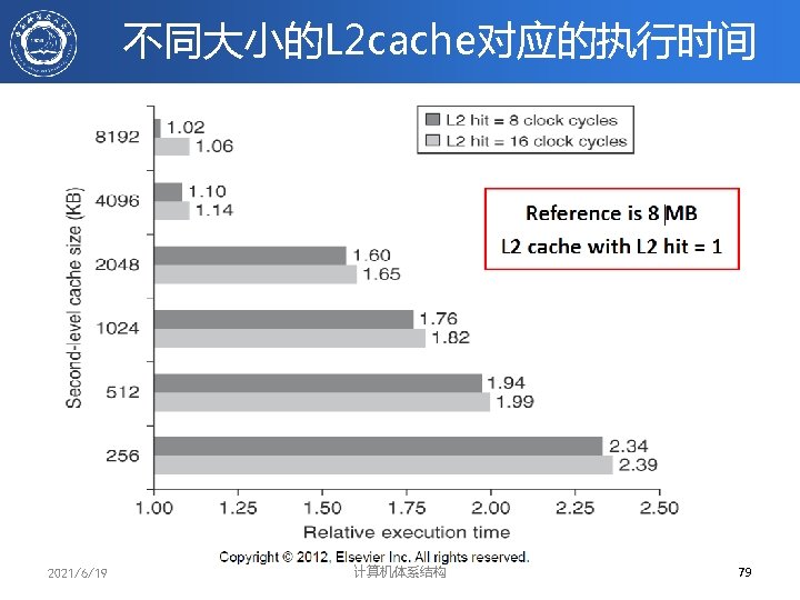
L 1 Size and Associativity Access time vs. size and associativity 2021/6/19 计算机体系结构 89
L 1 Size and Associativity Energy per read vs. size and associativity 2021/6/19 计算机体系结构 90
Nonblocking Cache Timeline 2021/6/19 计算机体系结构 97
Effectiveness of Non-Blocking Cache 2021/6/19 计算机体系结构 98
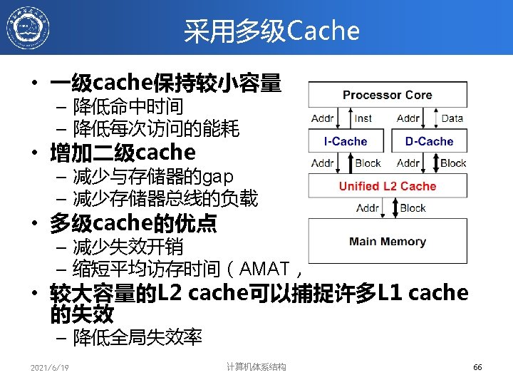
Multi-Ported Cache • Dual-Ported Data Cache – 两个地址端口(每个Cycle支持两条load/store 指令) – 在现代处理器中保持较高的指令吞吐率 • True Multi-ported Cache Design – 所有的控制和数据通路在Cache中是多份的 • Address Decoder, way multiplexor, tag comparator, aligners • Tag Array, Data Array – 显著地增加了Cache的面积和访问时间 • Multi-Banked Cache – 将cache组织成多个banks – 每个bank是一个端口 – 可以并行访问不同的Bank 2021/6/19 计算机体系结构 103
5、Multibanked Caches • 将Cache组织为多个独立的banks,以支持 并行访问 – ARM Cortex-A 8 supports 1 -4 banks for L 2 – Intel i 7 supports 4 banks for L 1 and 8 banks for L 2 • 根据块号进行顺序多体交叉编址 2021/6/19 计算机体系结构 104
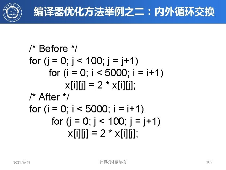
编译器优化方法举例之一:数组合并 // Original Code for (i = 0; i < N; i++) a[i] = b[i] + c[i]; for (i = 0; i < N; i++) d[i] = a[i] + b[i] * c[i]; Blocks are replaced in first loop then accessed in second // After Loop Fusion for (i = 0; i < N; i++) { a[i] = b[i] + c[i]; d[i] = a[i] + b[i] * c[i]; } Revised version takes advantage of temporal locality 2021/6/19 计算机体系结构 108
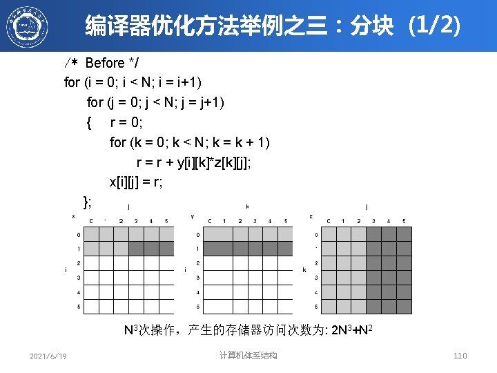
编译器优化方法举例之三:分块 (2/2) /* After */ for (jj = 0; jj < N; jj = jj+B) for (kk = 0; kk < N; kk = kk+B) for (i = 0; i < N; i = i+1) for (j = jj; j < min(jj+B, N); j = j+1) { r = 0; for (k = kk; k < min(kk+B, N); k = k + 1) r = r + y[i][k]*z[k][j]; x[i][j] = x[i][j] + r; }; 2021/6/19 计算机体系结构 111
硬件预取 Fetch two blocks on miss (include next sequential block) Pentium 4 Pre-fetching 2021/6/19 计算机体系结构 114
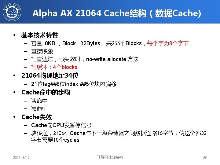
举例1 Example :For the code below, determine which accesses are likely to cause data cache misses. Next, insert prefetch instructions to reduce misses. Finally, calculate the number of prefetch instructions executed and the misses avoided by prefetching. Let’s assume we have an 8 KB direct-mapped data cache with 16 -byte blocks, and it is a write-back cache that does write allocate. The elements of a and b are 8 bytes long since they are double-precision floating-point arrays. There are 3 rows and 100 columns for a and 101 rows and 3 columns for b. Let’s also assume they are not in the cache at the start of the program. for (i = 0; i < 3; i = i+1) for (j = 0; j < 100; j = j+1) a[i][j] = b[j][0] * b[j+1][0]; 2021/6/19 计算机体系结构 117
for (j = 0; j < 100; j = j+1) { prefetch(b[j+7][0]); /* b(j, 0) for 7 iterations later */ prefetch(a[0][j+7]); /* a(0, j) for 7 iterations later */ a[0][j] = b[j][0] * b[j+1][0]; }; for (i = 1; i < 3; i = i+1) for (j = 0; j < 100; j = j+1) { prefetch(a[i][j+7]); /* a(i, j) for +7 iterations */ a[i][j] = b[j][0] * b[j+1][0]; } 2021/6/19 计算机体系结构 118
举例2 Example : Calculate the time saved in the example above. (1) Ignore instruction cache misses and assume there are no conflict or capacity misses in the data cache. (2) Assume that prefetches can overlap with each other and with cache misses, thereby transferring at the maximum memory bandwidth. (3) Here are the key loop times ignoring cache misses: The original loop takes 7 clock cycles per iteration, the first prefetch loop takes 9 clock cycles per iteration, and the second prefetch loop takes 8 clock cycles per iteration (including the overhead of the outer for loop). A miss takes 100 clock cycles. 119 计算机体系结构 2021/6/19
cache -review • 基本优化方法 – 扩大Cache容量 – 增大Cache块 – 提高相联度 – Victim Cache – 多级Cache – AMAT = Hit Time. L 1+Miss rate. L 1× (Hit Time. L 2+Miss rate. L 2×Miss penalty. L 2) – 让读失效优先于写写失效 • 10 种高级优化方法 2021/6/19 计算机体系结构 120
-review : Summary 2021/6/19 计算机体系结构 121
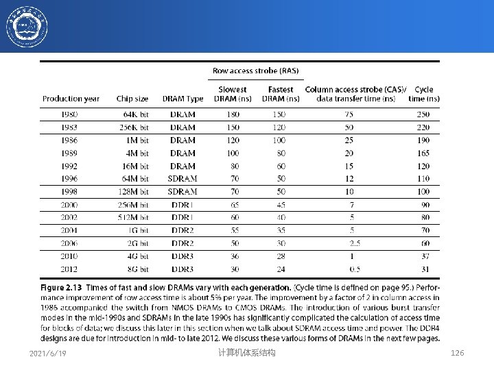
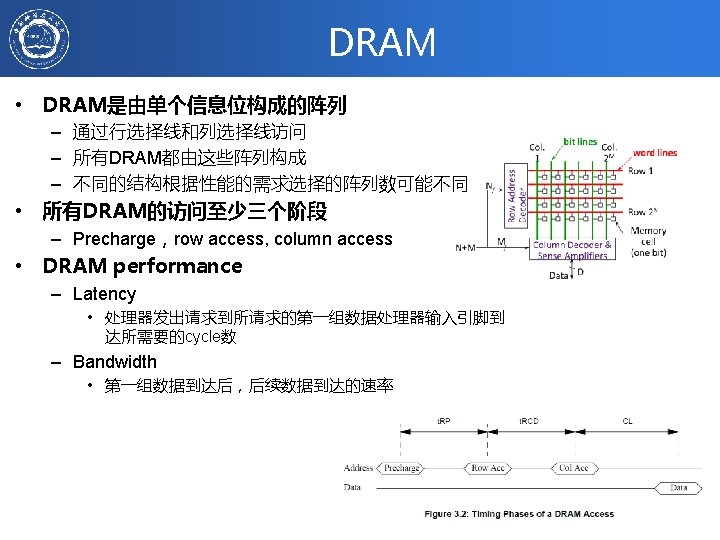
DRAM • DRAM – 破坏性读:读后需要重新写回, 必须要周期性的刷新 – 每位1个 transistor – 地址线复用: • Lower half of address: column access strobe (CAS) • Upper half of address: row access strobe (RAS) • SRAM – 每位6个transistors – 只需较低的功率来保持位状态 Col. 1 N+M 2021/6/19 Col. 2 M M word lines Row 1 Row Address Decoder N bit lines Row 2 N Column Decoder & Sense Amplifiers 计算机体系结构 Data D Memory cell (one bit) 123
DRAM Packaging (Laptops/Desktops/Servers) Clock and control signals ~7 Address lines multiplexed row/column address ~12 DRAM chip Data bus (4 b, 8 b, 16 b, 32 b) • • DIMM (Dual Inline Memory Module) contains multiple chips with clock/control/address signals connected in parallel (sometimes need buffers to drive signals to all chips) Data pins work together to return wide word (e. g. , 64 -bit data bus using 16 x 4 -bit parts) 2021/6/19 计算机体系结构 124
Memory 优化 • Some optimizations: Column Address – Fast Page Mode Operation N cols • Multiple accesses to same row – Synchronous DRAM • Added clock to DRAM interface • Burst mode with critical word first – Wider interfaces – Double data rate (DDR) – Multiple banks on each DRAM device N rows DRAM N x M “SRAM” M-bit Output 2021/6/19 计算机体系结构 Row Address M bits 125
Memory Optimizations 2021/6/19 计算机体系结构 127
• DDR: – DDR 2:Lower power (2. 5 V -> 1. 8 V),Higher clock rates (266 MHz, 333 MHz, 400 MHz) – DDR 3: 1. 5 V,800 MHz – DDR 4: 1 -1. 2 V,1600 MHz • GDDR 5 is graphics memory based on DDR 3 • Graphics memory: – Achieve 2 -5 X bandwidth per DRAM vs. DDR 3 • Wider interfaces (32 vs. 16 bit) • Higher clock rate 2021/6/19 计算机体系结构 128
3 D-Stacked DRAM and Processing in Memory (PIM)
Memory 功耗 Reducing power in SDRAMs: • Lower voltage • Low power mode (ignores clock, continues to refresh) Figure 2. 6 Power consumption for a DDR 3 SDRAM operating under three conditions: low-power (shutdown) mode, typical system mode (DRAM is active 30% of the time for reads and 15% for writes), and fully active mode, where the DRAM is continuously reading or writing. Reads and writes assume bursts of eight transfers. These data are based on a Micron 1. 5 V 2 GB DDR 3 -1066, although similar savings occur in DDR 4 SDRAMs 2021/6/19 计算机体系结构 130
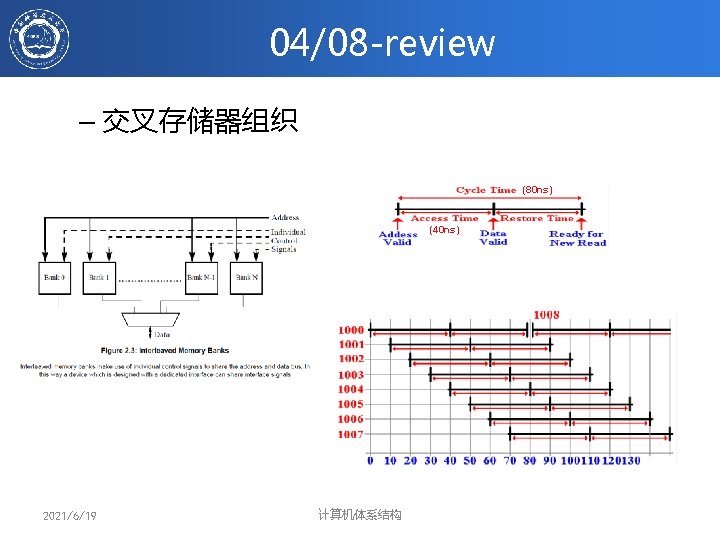
三种存储器组织方式 Interleaved: Wide: Simple: CPU/Mux 1 word; Mux/Cache, Bus, Memory N words (Alpha: 64 bits & 256 bits) CPU, Cache, Bus, Memory same width (32 bits) 2021/6/19 计算机体系结构 CPU, Cache, Bus 1 word: Memory N Modules (4 Modules); example is word interleaved 131
Increasing Bandwidth - Interleaving Access Pattern without Interleaving: D 1 available Start Access for D 1 CPU Memory Start Access for D 2 Memory Bank 0 Access Pattern with 4 -way Interleaving: CPU Memory Bank 1 Access Bank 0 Memory Bank 2 Access Bank 1 Access Bank 2 Access Bank 3 We can Access Bank 0 again 2021/6/19 计算机体系结构 Memory Bank 3 134
04/08 -review : Summary 2021/6/19 计算机体系结构 141
04/08 -review • 存储器组织 – 存储系统结构 参考文献 Davis, B. T. (2001). Modern dram architectures, University of Michigan: 221. Jacob, B. (2009). The Memory System, Morgan & Claypool. 2021/6/19 计算机体系结构 142
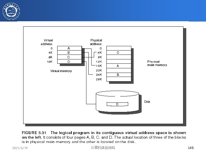
Alpha VPN->PPN 2021/6/19 计算机体系结构 154
TLB的典型参数 • block size - same as a page table entry - 1 or 2 words • hit time - 1 cycle • miss penalty - 10 to 30 cycles • miss rate -. 1% to 2% • TLB size - 32 B to 8 KB 2021/6/19 计算机体系结构 156
举例:Alpha 21064的TLB 2021/6/19 计算机体系结构 157
Summary of Virtual Memory and Caches 2021/6/19 计算机体系结构 158
Acknowledgements • These slides contain material developed and copyright by: – John Kubiatowicz (UCB) – Krste Asanovic (UCB) – David Patterson (UCB) – Chenxi Zhang (Tongji) • UCB material derived from course CS 152、CS 252、CS 61 C • KFUPM material derived from course COE 501、COE 502 6/19/2021 159
DRAM的演进 • • • DRAM Fast-page-mode (FPM) Extended-data-out (EDO) Burst-EDO (BEDO) Synchronous DRAM (SDRAM) – Single-data-rate (SDR) SDRAM – Double-data-rate (DDR) SDRAM, DDR 2 – Rambus DRAM (RDRAM) – Direct Rambus DRAM (DRDRAM)
Acknowledgements • These slides contain material developed and copyright by: – John Kubiatowicz (UCB) – Krste Asanovic (UCB) – John Hennessy (Standford)and David Patterson (UCB) – Chenxi Zhang (Tongji) – Muhamed Mudawar (KFUPM) • UCB material derived from course CS 152、CS 252、CS 61 C • KFUPM material derived from course COE 501、COE 502 6/19/2021 162
-review • Cache基本原理 4 Q • Cache性能分析 CPU time = (CPU execution clock cycles + Memory stall clock cycles) x clock cycle time Memory stall clock cycles = (Reads x Read miss rate x Read miss penalty + Writes x Write miss rate x Write miss penalty) Memory stall clock cycles = Memory accesses x Miss rate x Miss penalty Different measure: AMAT Average Memory Access time (AMAT) = Hit Time + (Miss Rate x Miss Penalty) 2021/6/19 计算机体系结构 163
0 2 2 4 4 6 6 1 1 3 3 5 5 3 -- -- -- 0 -- 1 0 1 4 - 4 5 2 -- 2 3 2 -— ??? set 0 Write Back 0 和1 0 1 2 3 4 5 6 7 0(0) 0(1) 1(2) 1(3) 2(4) 2(5) 3(6) 8 3(7) 9 4(8) 10 4(9) 11 5(10) 2021/6/19 • • L 1: 1 -way L 2: 2 -way L 1和L 2的块大小不同,L 1的block. Size是L 2的block. Size的 1/2 替换策略:LRU 考察按L 1的块划分的访问序列: 0123456 3 (L 2 #5与L 1中的#3互换) 计算机体系结构 165