Main Memory System Nam Sung Kim Dept of

- Slides: 50

Main Memory System Nam Sung Kim Dept. of Electrical and Computer Engineering University of Illinois-Urbana Champaign Acknowledgement: Many slides were adapted from Prof. Mutulu’s ECE 740 Computer Architecture at CMU with his generous permission. ECE 511 Computer Architecture

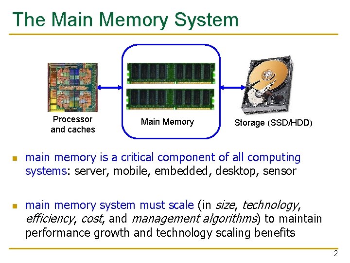
The Main Memory System Processor and caches n n Main Memory Storage (SSD/HDD) main memory is a critical component of all computing systems: server, mobile, embedded, desktop, sensor main memory system must scale (in size, technology, efficiency, cost, and management algorithms) to maintain performance growth and technology scaling benefits 2

State of the Main Memory System n recent technology, architecture, and application trends q q n n n lead to new requirements exacerbate old requirements DRAM and memory controllers, as we know them today, are (will be) unlikely to satisfy all requirements some emerging non-volatile memory technologies (e. g. , PCM) enable new opportunities: memory+storage merging we need to rethink the main memory system q q to fix DRAM issues and enable emerging technologies to satisfy all requirements 3

Major Trends Affecting Main Memory (I) n need for main memory w/ high capacity and bandwidth n main memory energy/power is a key system design concern n DRAM technology scaling is ending 4

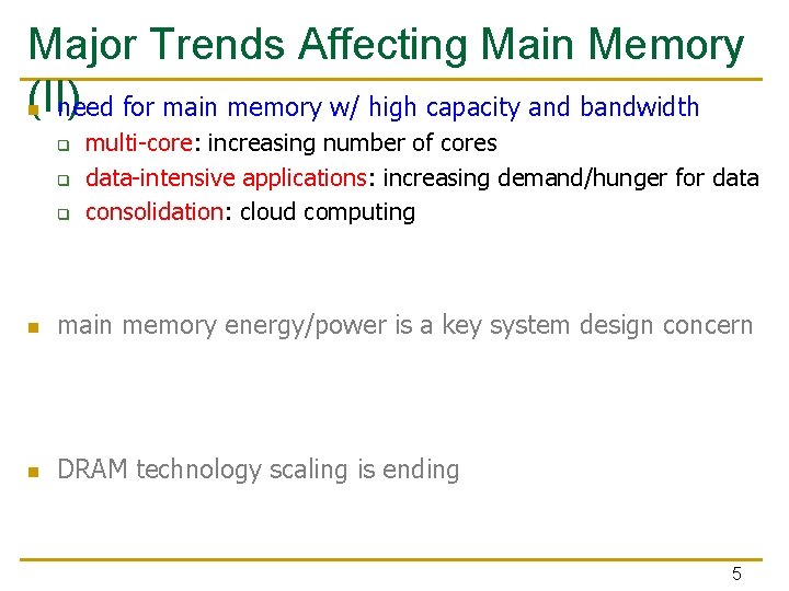
Major Trends Affecting Main Memory (II) n need for main memory w/ high capacity and bandwidth q q q multi-core: increasing number of cores data-intensive applications: increasing demand/hunger for data consolidation: cloud computing n main memory energy/power is a key system design concern n DRAM technology scaling is ending 5

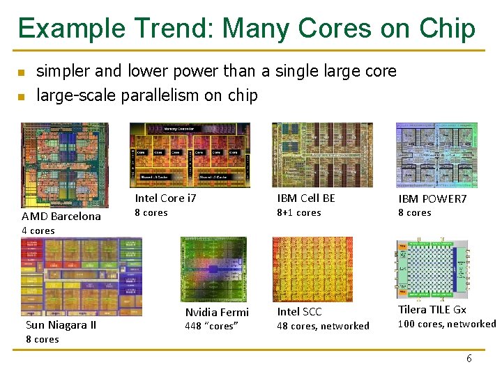
Example Trend: Many Cores on Chip n n simpler and lower power than a single large core large-scale parallelism on chip Intel Core i 7 AMD Barcelona 8 cores IBM Cell BE IBM POWER 7 Intel SCC Tilera TILE Gx 8+1 cores 8 cores 4 cores Sun Niagara II 8 cores Nvidia Fermi 448 “cores” 48 cores, networked 100 cores, networked 6

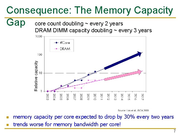
Consequence: The Memory Capacity Gap core count doubling ~ every 2 years DRAM DIMM capacity doubling ~ every 3 years n n memory capacity per core expected to drop by 30% every two years trends worse for memory bandwidth per core! 7

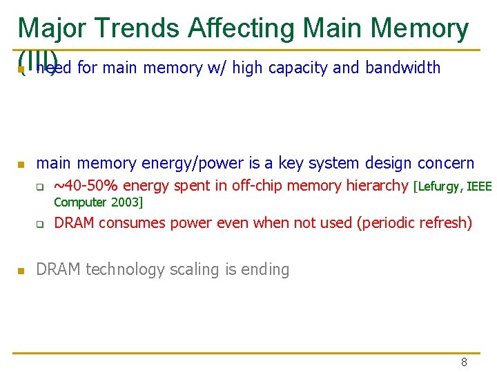
Major Trends Affecting Main Memory (III) n need for main memory w/ high capacity and bandwidth n main memory energy/power is a key system design concern q ~40 -50% energy spent in off-chip memory hierarchy [Lefurgy, IEEE Computer 2003] q n DRAM consumes power even when not used (periodic refresh) DRAM technology scaling is ending 8

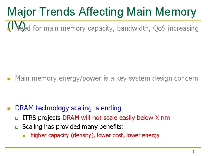
Major Trends Affecting Main Memory (IV) n Need for main memory capacity, bandwidth, Qo. S increasing n Main memory energy/power is a key system design concern n DRAM technology scaling is ending q q ITRS projects DRAM will not scale easily below X nm Scaling has provided many benefits: n higher capacity (density), lower cost, lower energy 9

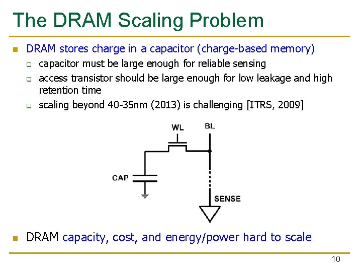
The DRAM Scaling Problem n DRAM stores charge in a capacitor (charge-based memory) q q q n capacitor must be large enough for reliable sensing access transistor should be large enough for low leakage and high retention time scaling beyond 40 -35 nm (2013) is challenging [ITRS, 2009] DRAM capacity, cost, and energy/power hard to scale 10

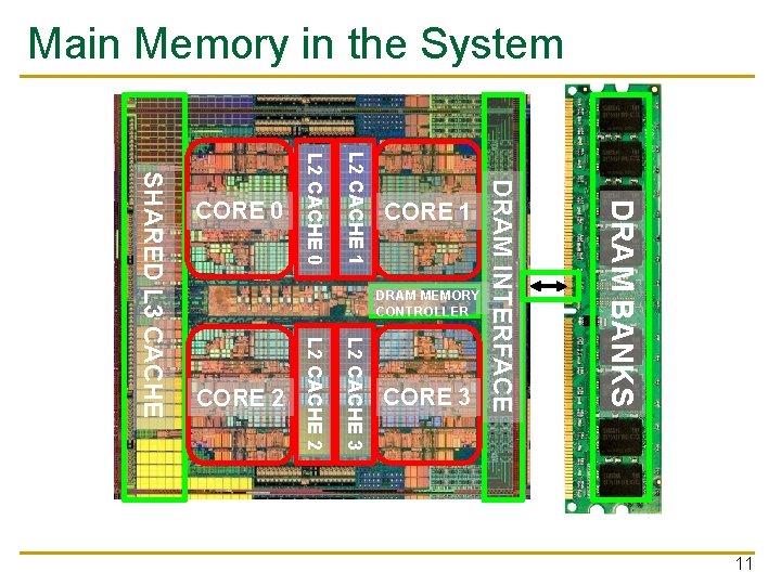
Main Memory in the System DRAM BANKS L 2 CACHE 3 L 2 CACHE 2 SHARED L 3 CACHE DRAM MEMORY CONTROLLER DRAM INTERFACE L 2 CACHE 1 L 2 CACHE 0 CORE 3 CORE 2 CORE 1 CORE 0 11

Ideal Memory n n zero access time (latency) infinite capacity zero cost infinite bandwidth (to support multiple accesses in parallel) 12

The Problem n ideal memory’s requirements oppose each other n bigger is slower q n faster is more expensive q n bigger Takes longer to determine the location memory technology: SRAM vs. DRAM higher bandwidth is more expensive q need more banks, more ports, higher frequency, or faster technology 13

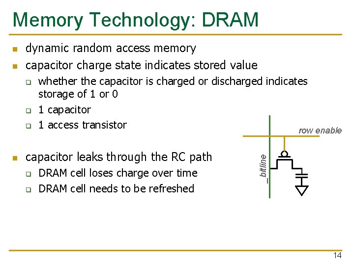
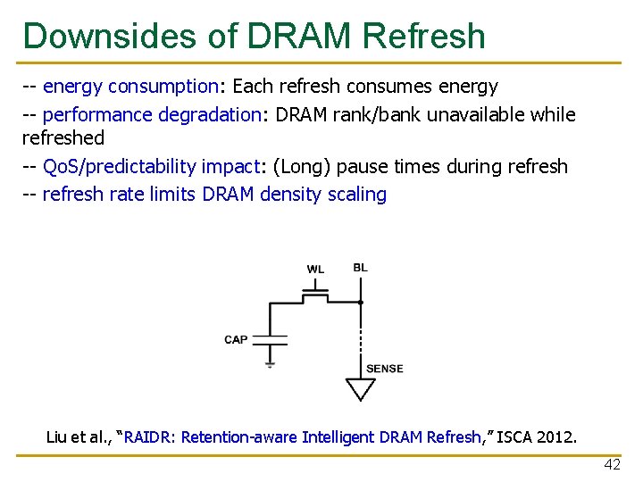
Memory Technology: DRAM n dynamic random access memory capacitor charge state indicates stored value q q q n whether the capacitor is charged or discharged indicates storage of 1 or 0 1 capacitor 1 access transistor row enable capacitor leaks through the RC path q q DRAM cell loses charge over time DRAM cell needs to be refreshed _bitline n 14

The DRAM Subsystem

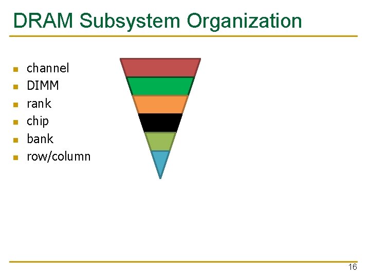
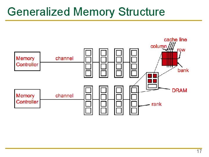
DRAM Subsystem Organization n n n channel DIMM rank chip bank row/column 16

Generalized Memory Structure 17

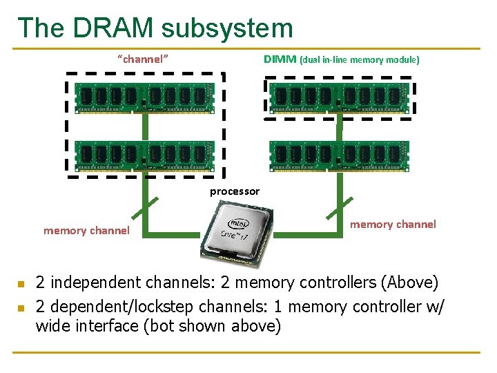
The DRAM subsystem “channel” DIMM (dual in-line memory module) processor memory channel n n memory channel 2 independent channels: 2 memory controllers (Above) 2 dependent/lockstep channels: 1 memory controller w/ wide interface (bot shown above)

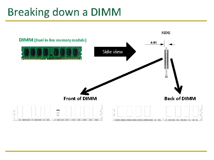
Breaking down a DIMM (Dual in-line memory module) Side view Front of DIMM Back of DIMM

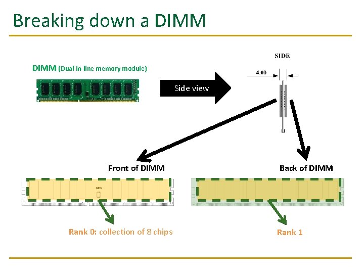
Breaking down a DIMM (Dual in-line memory module) Side view Front of DIMM Rank 0: collection of 8 chips Back of DIMM Rank 1

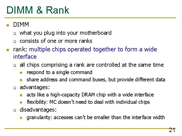
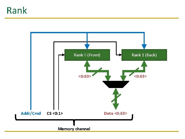
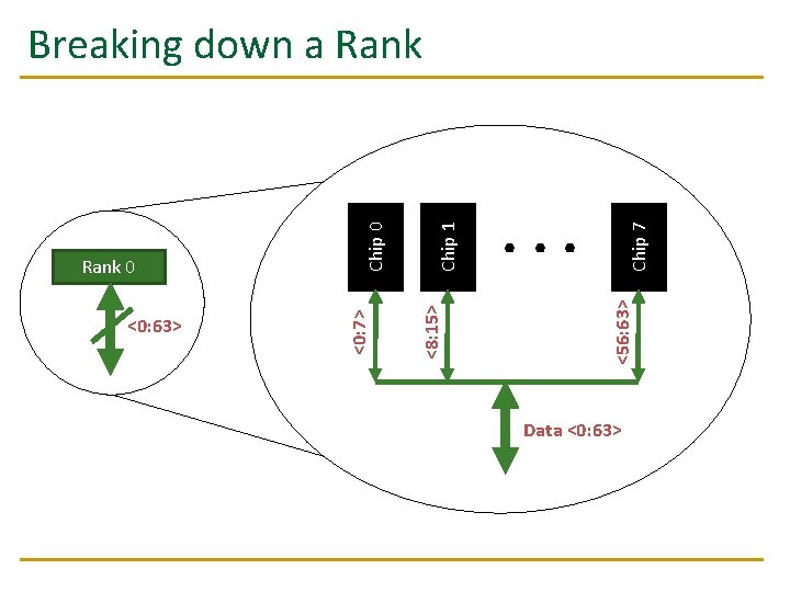
DIMM & Rank n DIMM q q n what you plug into your motherboard consists of one or more ranks rank: multiple chips operated together to form a wide interface q all chips comprising a rank are controlled at the same time n n q advantages: n n q respond to a single command share address and command buses, but provide different data acts like a high-capacity DRAM chip with a wide interface flexibility: MC doesn’t need to deal with individual chips disadvantages: n granularity: accesses can’t be smaller than the interface width 21

Rank 0 (Front) Rank 1 (Back) <0: 63> Addr/Cmd CS <0: 1> Memory channel <0: 63> Data <0: 63>

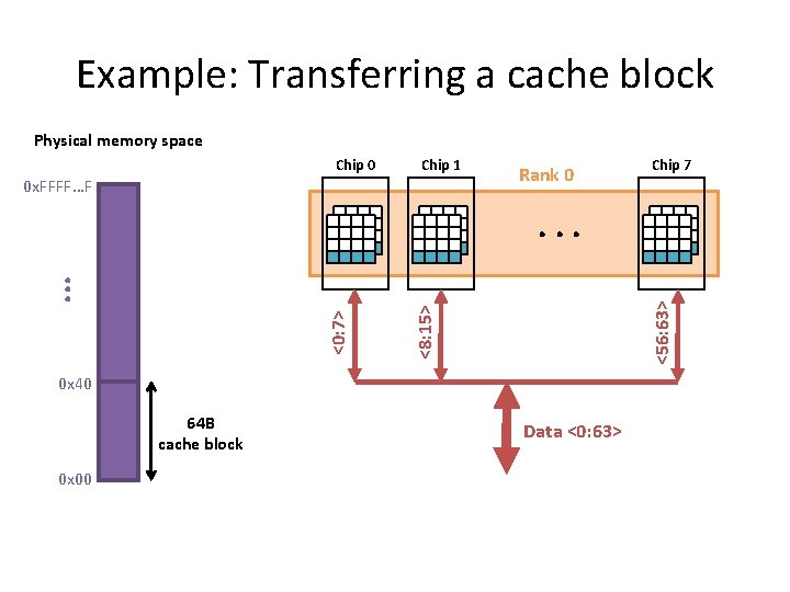
Chip 7 . . . <56: 63> Chip 1 <8: 15> <0: 63> <0: 7> Rank 0 Chip 0 Breaking down a Rank Data <0: 63>

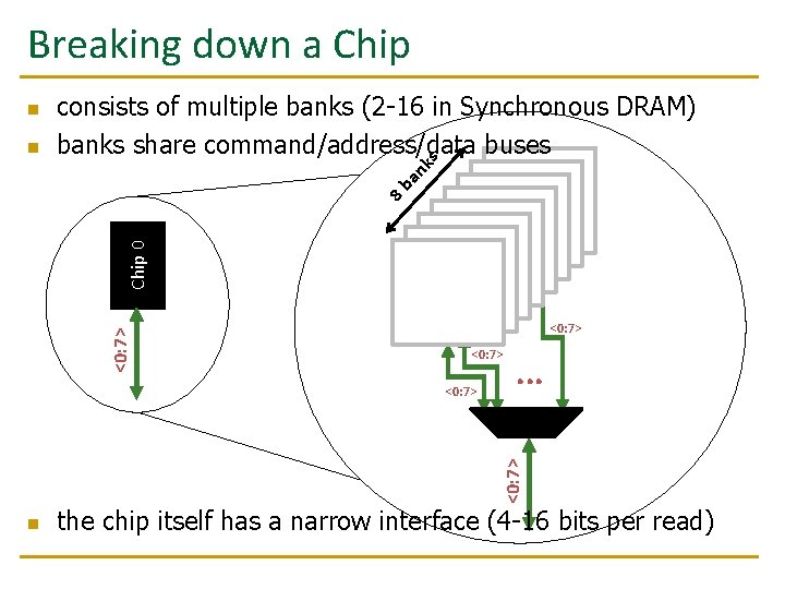
Breaking down a Chip n <0: 7> Chip 0 8 b an ks n consists of multiple banks (2 -16 in Synchronous DRAM) banks share command/address/data buses Bank 0 <0: 7> . . . <0: 7> n the chip itself has a narrow interface (4 -16 bits per read)

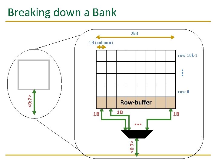
Breaking down a Bank 2 k. B 1 B (column) row 16 k-1 . . . Bank 0 <0: 7> row 0 Row-buffer 1 B . . . <0: 7> 1 B 1 B

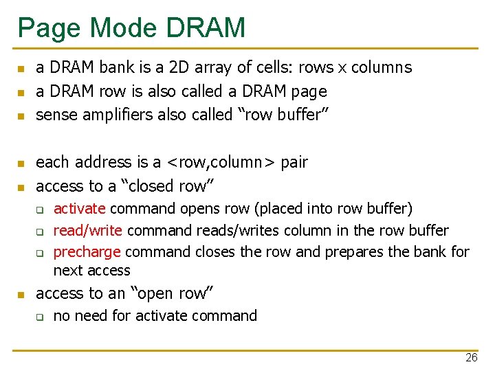
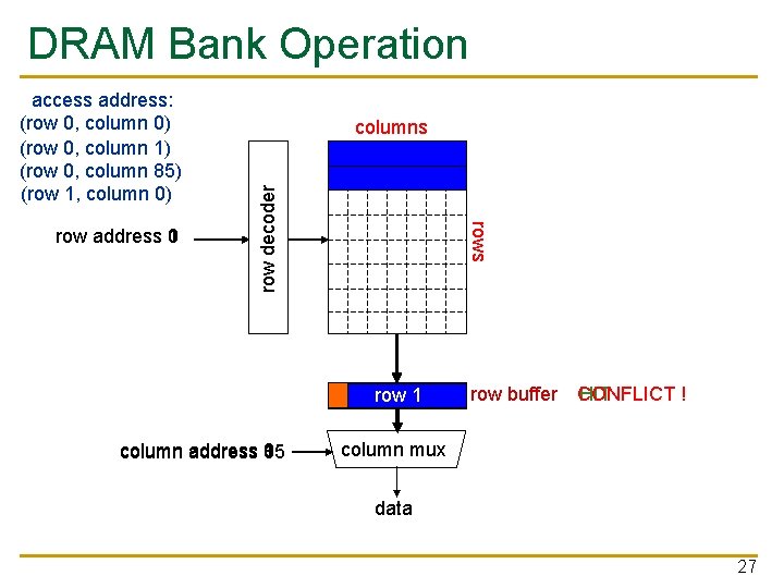
Page Mode DRAM n n n a DRAM bank is a 2 D array of cells: rows x columns a DRAM row is also called a DRAM page sense amplifiers also called “row buffer” each address is a <row, column> pair access to a “closed row” q q q n activate command opens row (placed into row buffer) read/write command reads/writes column in the row buffer precharge command closes the row and prepares the bank for next access to an “open row” q no need for activate command 26

DRAM Bank Operation rows row address 1 0 columns row decoder access address: (row 0, column 0) (row 0, column 1) (row 0, column 85) (row 1, column 0) row 01 empty row column address 0 1 85 row buffer CONFLICT HIT ! column mux data 27

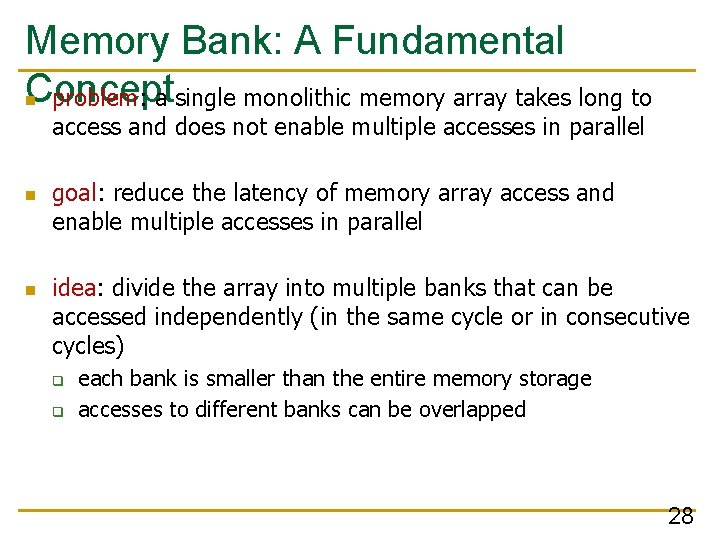
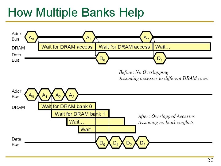
Memory Bank: A Fundamental Concept n problem: a single monolithic memory array takes long to access and does not enable multiple accesses in parallel n n goal: reduce the latency of memory array access and enable multiple accesses in parallel idea: divide the array into multiple banks that can be accessed independently (in the same cycle or in consecutive cycles) q q each bank is smaller than the entire memory storage accesses to different banks can be overlapped 28

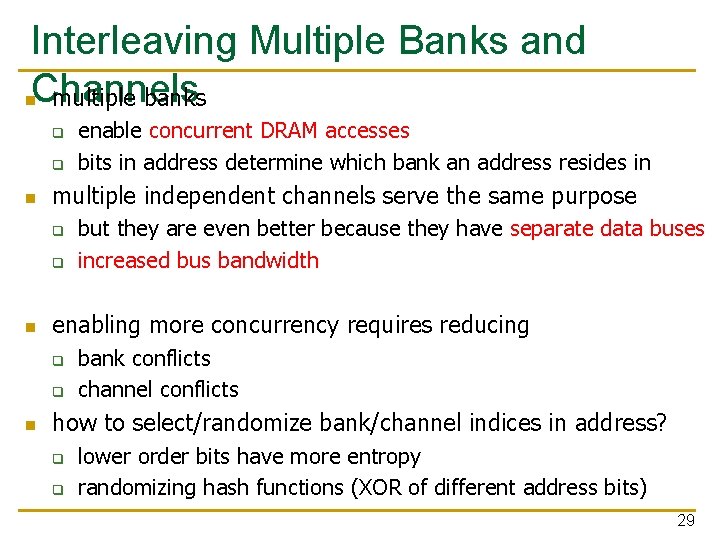
Interleaving Multiple Banks and n. Channels multiple banks q q n multiple independent channels serve the same purpose q q n but they are even better because they have separate data buses increased bus bandwidth enabling more concurrency requires reducing q q n enable concurrent DRAM accesses bits in address determine which bank an address resides in bank conflicts channel conflicts how to select/randomize bank/channel indices in address? q q lower order bits have more entropy randomizing hash functions (XOR of different address bits) 29

How Multiple Banks Help 30

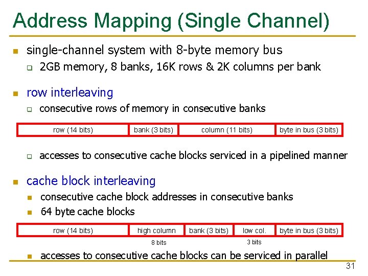
Address Mapping (Single Channel) n single-channel system with 8 -byte memory bus q n 2 GB memory, 8 banks, 16 K rows & 2 K columns per bank row interleaving q consecutive rows of memory in consecutive banks row (14 bits) q n bank (3 bits) column (11 bits) byte in bus (3 bits) accesses to consecutive cache blocks serviced in a pipelined manner cache block interleaving n n consecutive cache block addresses in consecutive banks 64 byte cache blocks row (14 bits) high column 8 bits n bank (3 bits) low col. byte in bus (3 bits) 3 bits accesses to consecutive cache blocks can be serviced in parallel 31

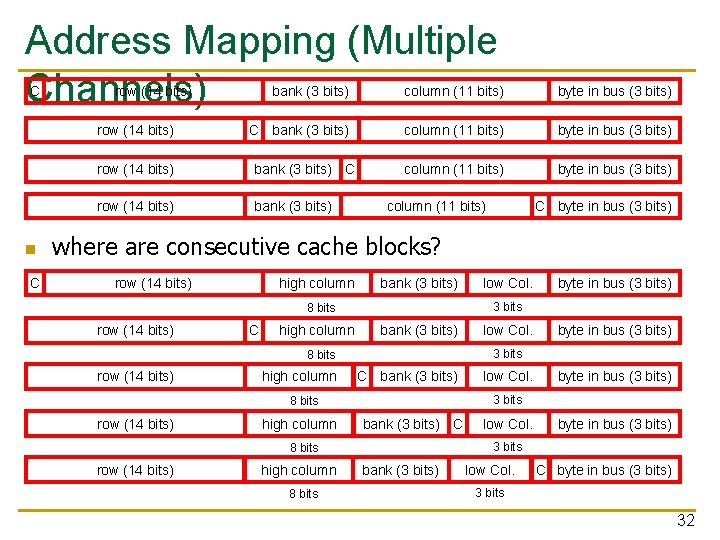
Address Mapping (Multiple Channels) C row (14 bits) n C bank (3 bits) column (11 bits) byte in bus (3 bits) row (14 bits) bank (3 bits) C row (14 bits) bank (3 bits) column (11 bits) C byte in bus (3 bits) where are consecutive cache blocks? row (14 bits) high column bank (3 bits) C high column bank (3 bits) high column C bank (3 bits) high column bank (3 bits) C high column 8 bits low Col. byte in bus (3 bits) 3 bits 8 bits row (14 bits) low Col. bank (3 bits) low Col. C byte in bus (3 bits) 3 bits 32

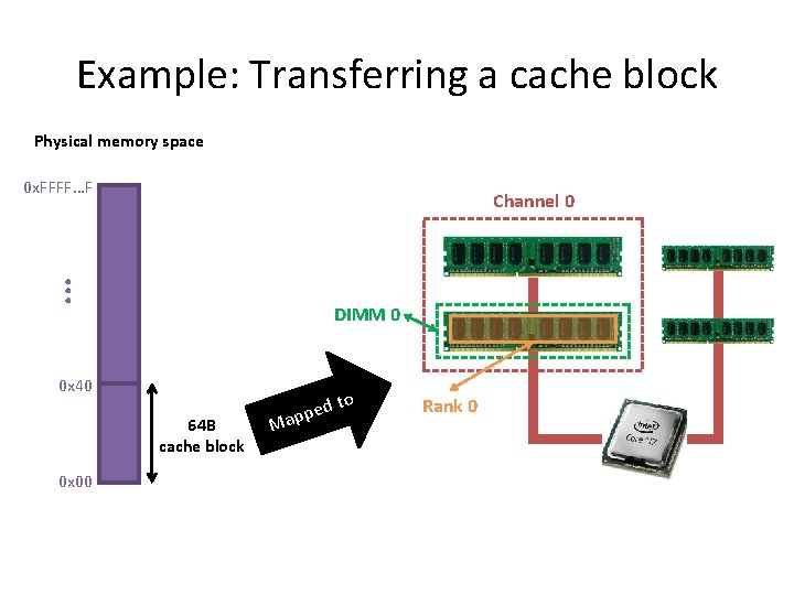
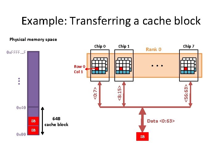
Example: Transferring a cache block Physical memory space 0 x. FFFF…F . . . Channel 0 DIMM 0 0 x 40 64 B cache block 0 x 00 to d e p Map Rank 0

Example: Transferring a cache block Physical memory space Chip 0 Chip 1 0 x. FFFF…F Rank 0 Chip 7 <56: 63> <8: 15> <0: 7> . . . 0 x 40 64 B cache block 0 x 00 Data <0: 63>

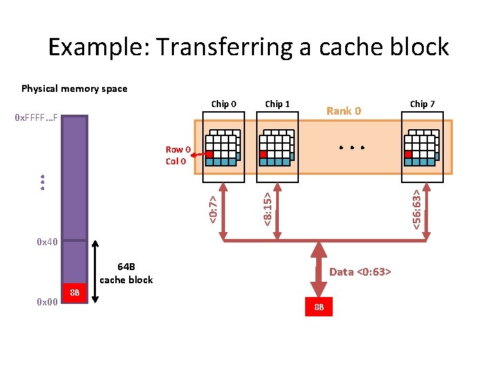
Example: Transferring a cache block Physical memory space Chip 0 Chip 1 0 x. FFFF…F Rank 0 . . . <56: 63> <8: 15> <0: 7> . . . Row 0 Col 0 0 x 40 64 B cache block 0 x 00 Chip 7 Data <0: 63>

Example: Transferring a cache block Physical memory space Chip 0 Chip 1 Rank 0 0 x. FFFF…F . . . <56: 63> <8: 15> <0: 7> . . . Row 0 Col 0 0 x 40 64 B cache block 0 x 00 Chip 7 Data <0: 63> 8 B 8 B

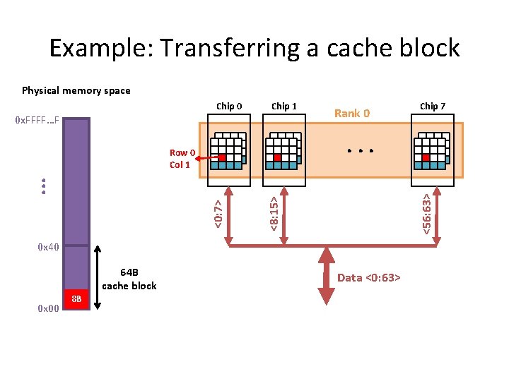
Example: Transferring a cache block Physical memory space Chip 0 Chip 1 0 x. FFFF…F Rank 0 . . . <56: 63> <8: 15> <0: 7> . . . Row 0 Col 1 0 x 40 64 B cache block 0 x 00 8 B Chip 7 Data <0: 63>

Example: Transferring a cache block Physical memory space Chip 0 Chip 1 Rank 0 0 x. FFFF…F . . . <56: 63> <8: 15> <0: 7> . . . Row 0 Col 1 0 x 40 8 B 0 x 00 Chip 7 64 B cache block Data <0: 63> 8 B 8 B

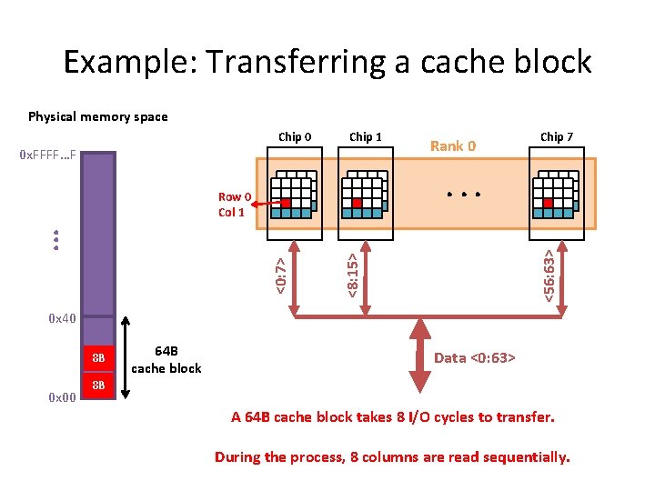
Example: Transferring a cache block Physical memory space Chip 0 Chip 1 0 x. FFFF…F Rank 0 Chip 7 . . . <56: 63> <8: 15> <0: 7> . . . Row 0 Col 1 0 x 40 8 B 0 x 00 64 B cache block Data <0: 63> 8 B A 64 B cache block takes 8 I/O cycles to transfer. During the process, 8 columns are read sequentially.

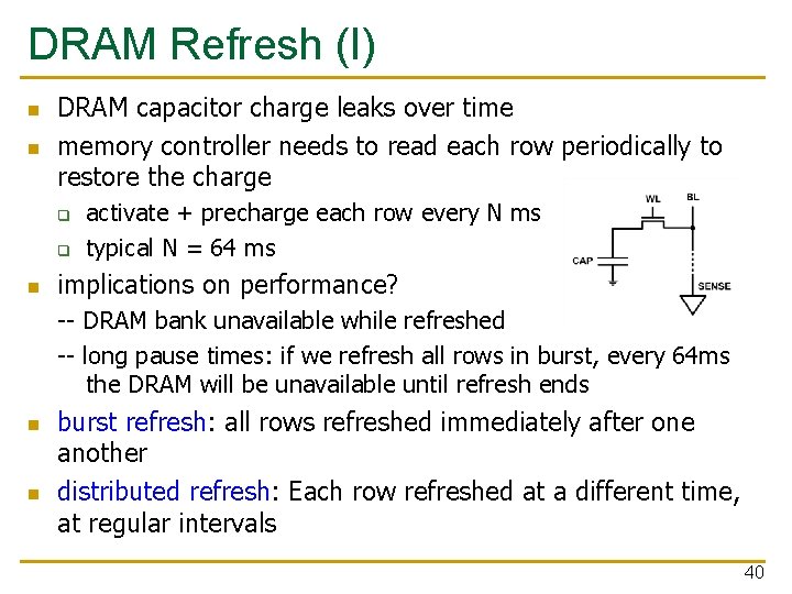
DRAM Refresh (I) n n DRAM capacitor charge leaks over time memory controller needs to read each row periodically to restore the charge q q n activate + precharge each row every N ms typical N = 64 ms implications on performance? -- DRAM bank unavailable while refreshed -- long pause times: if we refresh all rows in burst, every 64 ms the DRAM will be unavailable until refresh ends n n burst refresh: all rows refreshed immediately after one another distributed refresh: Each row refreshed at a different time, at regular intervals 40

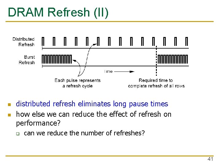
DRAM Refresh (II) n n distributed refresh eliminates long pause times how else we can reduce the effect of refresh on performance? q can we reduce the number of refreshes? 41

Downsides of DRAM Refresh -- energy consumption: Each refresh consumes energy -- performance degradation: DRAM rank/bank unavailable while refreshed -- Qo. S/predictability impact: (Long) pause times during refresh -- refresh rate limits DRAM density scaling Liu et al. , “RAIDR: Retention-aware Intelligent DRAM Refresh, ” ISCA 2012. 42

Memory Controllers

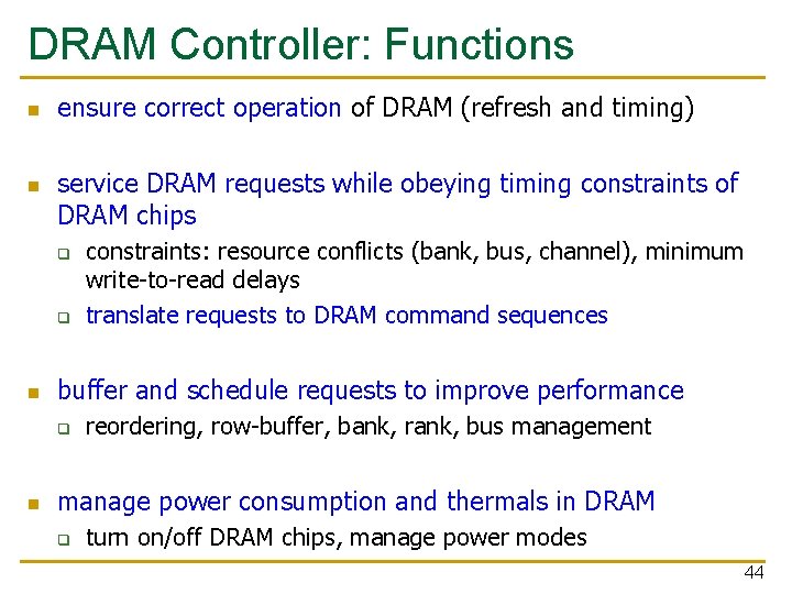
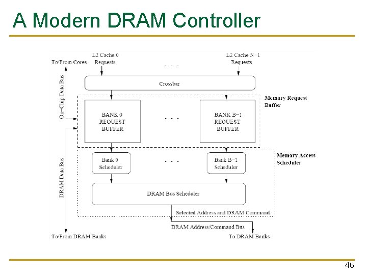
DRAM Controller: Functions n n ensure correct operation of DRAM (refresh and timing) service DRAM requests while obeying timing constraints of DRAM chips q q n buffer and schedule requests to improve performance q n constraints: resource conflicts (bank, bus, channel), minimum write-to-read delays translate requests to DRAM command sequences reordering, row-buffer, bank, rank, bus management manage power consumption and thermals in DRAM q turn on/off DRAM chips, manage power modes 44

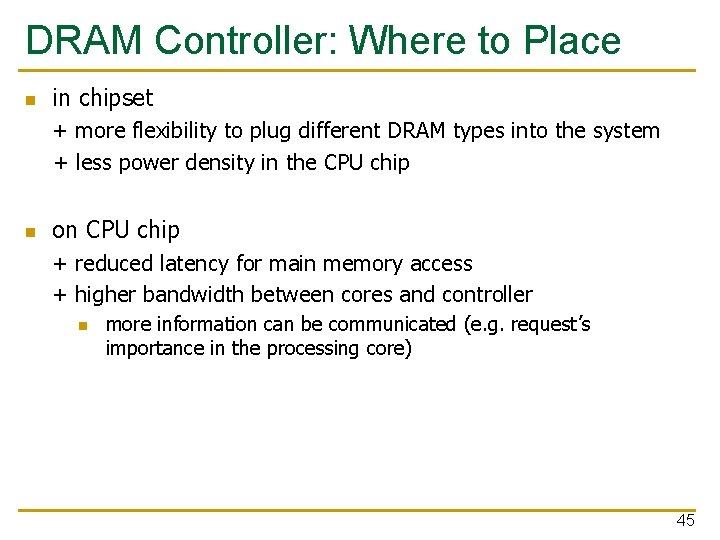
DRAM Controller: Where to Place n in chipset + more flexibility to plug different DRAM types into the system + less power density in the CPU chip n on CPU chip + reduced latency for main memory access + higher bandwidth between cores and controller n more information can be communicated (e. g. request’s importance in the processing core) 45

A Modern DRAM Controller 46

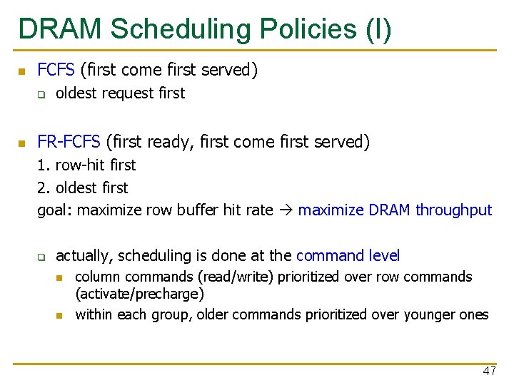
DRAM Scheduling Policies (I) n FCFS (first come first served) q n oldest request first FR-FCFS (first ready, first come first served) 1. row-hit first 2. oldest first goal: maximize row buffer hit rate maximize DRAM throughput q actually, scheduling is done at the command level n n column commands (read/write) prioritized over row commands (activate/precharge) within each group, older commands prioritized over younger ones 47

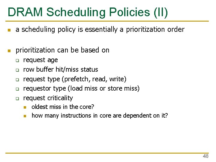
DRAM Scheduling Policies (II) n a scheduling policy is essentially a prioritization order n prioritization can be based on q q q request age row buffer hit/miss status request type (prefetch, read, write) requestor type (load miss or store miss) request criticality n n oldest miss in the core? how many instructions in core are dependent on it? 48

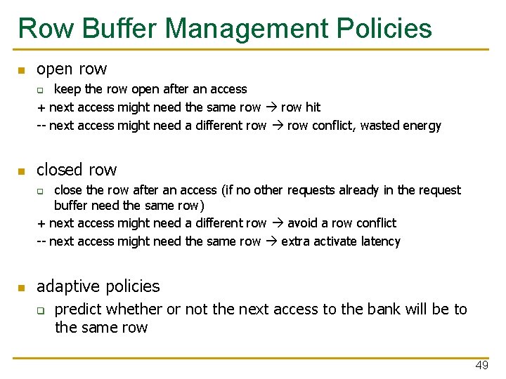
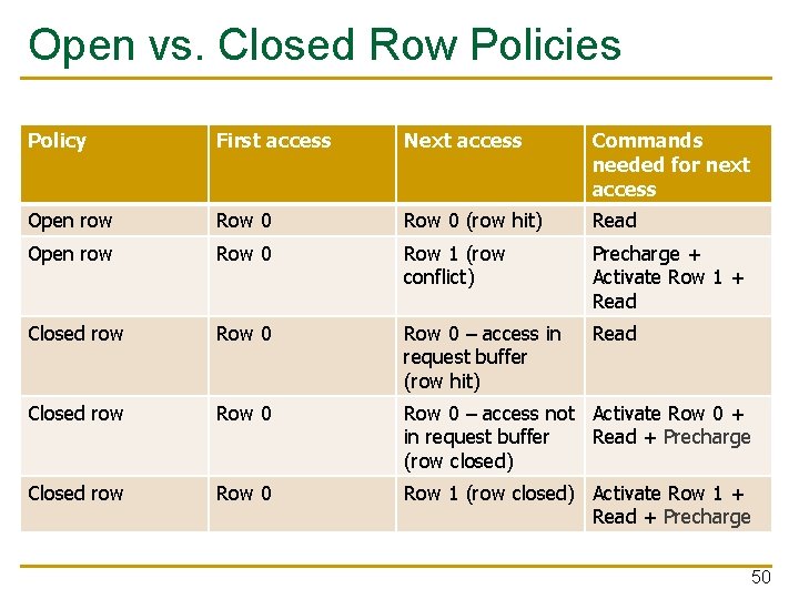
Row Buffer Management Policies n open row keep the row open after an access + next access might need the same row hit -- next access might need a different row conflict, wasted energy q n closed row close the row after an access (if no other requests already in the request buffer need the same row) + next access might need a different row avoid a row conflict -- next access might need the same row extra activate latency q n adaptive policies q predict whether or not the next access to the bank will be to the same row 49

Open vs. Closed Row Policies Policy First access Next access Commands needed for next access Open row Row 0 (row hit) Read Open row Row 0 Row 1 (row conflict) Precharge + Activate Row 1 + Read Closed row Row 0 – access in request buffer (row hit) Read Closed row Row 0 – access not Activate Row 0 + in request buffer Read + Precharge (row closed) Closed row Row 0 Row 1 (row closed) Activate Row 1 + Read + Precharge 50