Slide 1 Jan 2002 Taking the Mystery out








- Slides: 51

Slide - 1 Jan 2002 Taking the Mystery out of Signal Integrity Dr. Eric Bogatin, CTO, Giga. Test Labs eric@gigatest. com Signal Integrity Engineering and Training 134 S. Wolfe Rd Sunnyvale, CA 94086 408 -524 -2700 www. Giga. Test. com Copies of this presentation are available for download from www. Giga. Test. com www. Agilent. com/find/SI

Slide - 2 Overview “There are two kinds of design engineers, those that have signal integrity problems, and those that will” • The four signal integrity problems • Why signal integrity will get harder to solve • The right design methodology • The role of accurate, high bandwidth measurements • Two case studies: switching noise, probing

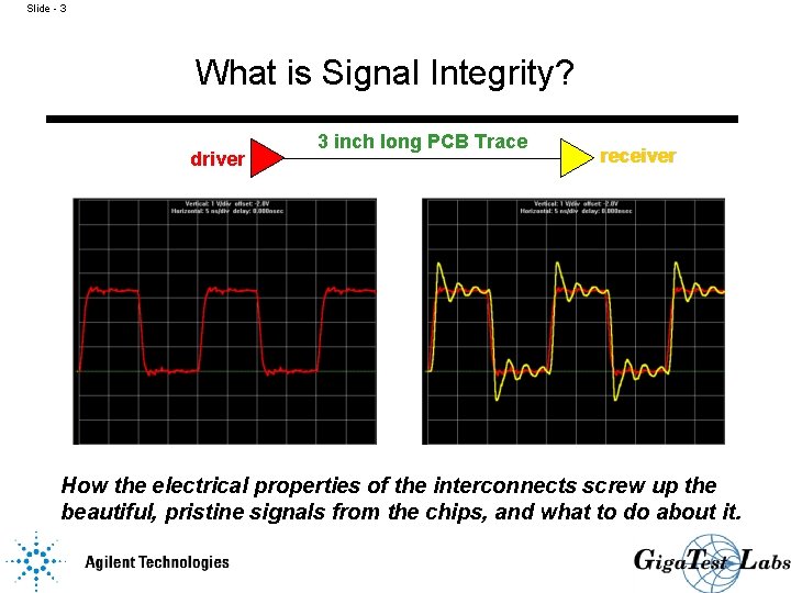
Slide - 3 What is Signal Integrity? driver 3 inch long PCB Trace receiver How the electrical properties of the interconnects screw up the beautiful, pristine signals from the chips, and what to do about it.

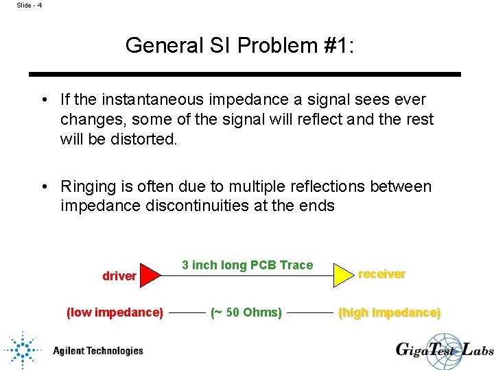
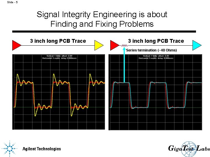
Slide - 4 General SI Problem #1: • If the instantaneous impedance a signal sees ever changes, some of the signal will reflect and the rest will be distorted. • Ringing is often due to multiple reflections between impedance discontinuities at the ends driver (low impedance) 3 inch long PCB Trace (~ 50 Ohms) receiver (high impedance)

Slide - 5 Signal Integrity Engineering is about Finding and Fixing Problems 3 inch long PCB Trace Series termination (~40 Ohms)

Slide - 6 A Guiding Principle In order to solve a signal integrity problem you must first understand its root cause

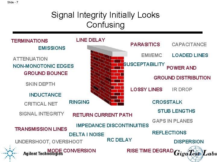
Slide - 7 Signal Integrity Initially Looks Confusing LINE DELAY TERMINATIONS EMISSIONS PARASITICS EMI/EMC ATTENUATION NON-MONOTONIC EDGES SUSCEPTABILITY GROUND BOUNCE CAPACITANCE LOADED LINES POWER AND GROUND DISTRIBUTION SKIN DEPTH LOSSY LINES IR DROP INDUCTANCE CRITICAL NET SIGNAL INTEGRITY TRANSMISSION LINES RINGING CROSSTALK RETURN CURRENT PATH IMPEDANCE DISCONTINUITIES DELTA I NOISE RC DELAY UNDERSHOOT, OVERSHOOT MODE CONVERSION STUB LENGTHS GAPS IN PLANES REFLECTIONS DISPERSION RISE TIME DEGRADATION

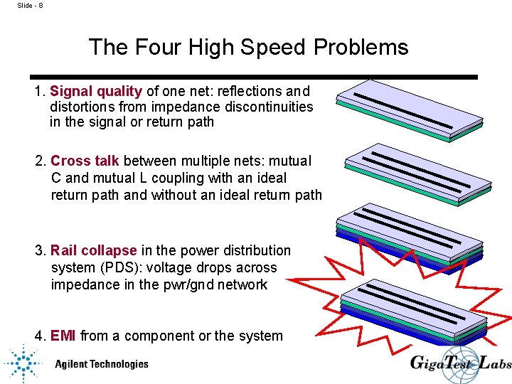
Slide - 8 The Four High Speed Problems 1. Signal quality of one net: reflections and distortions from impedance discontinuities in the signal or return path 2. Cross talk between multiple nets: mutual C and mutual L coupling with an ideal return path and without an ideal return path 3. Rail collapse in the power distribution system (PDS): voltage drops across impedance in the pwr/gnd network 4. EMI from a component or the system

Slide - 9 See additional Notes

Slide - 10 See additional Notes

Slide - 11 See additional Notes

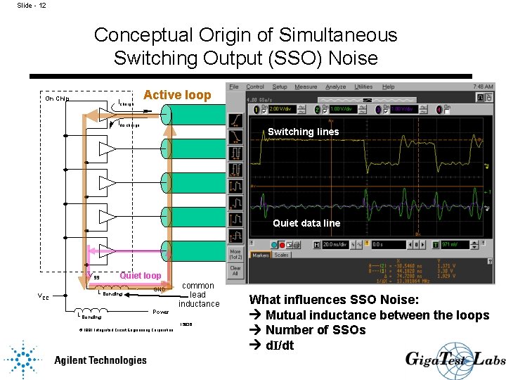
Slide - 12 Conceptual Origin of Simultaneous Switching Output (SSO) Noise On Chip Icharge Active loop Idischarge Switching lines Quiet data line V SS V CC Quiet loop L Bonding GND common lead inductance Power 15836 © 1991 Integrated Circuit Engineering Corporation What influences SSO Noise: Mutual inductance between the loops Number of SSOs d. I/dt

Slide - 13 See additional Notes

Slide - 14 See additional Notes

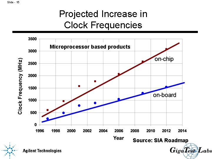
Slide - 15 Projected Increase in Clock Frequencies Microprocessor based products Source: SIA Roadmap

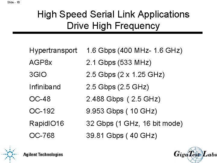
Slide - 16 High Speed Serial Link Applications Drive High Frequency Hypertransport 1. 6 Gbps (400 MHz- 1. 6 GHz) AGP 8 x 2. 1 Gbps (533 MHz) 3 GIO 2. 5 Gbps (2 x 1. 25 GHz) Infiniband 2. 5 Gbps (2. 5 GHz) OC-48 2. 488 Gbps ( 2. 5 GHz) OC-192 9. 953 Gbps ( 10 GHz) Rapid. IO 16 32 Gbps (1 GHz, 16 bit mode) OC-768 39. 81 Gbps ( 40 GHz)

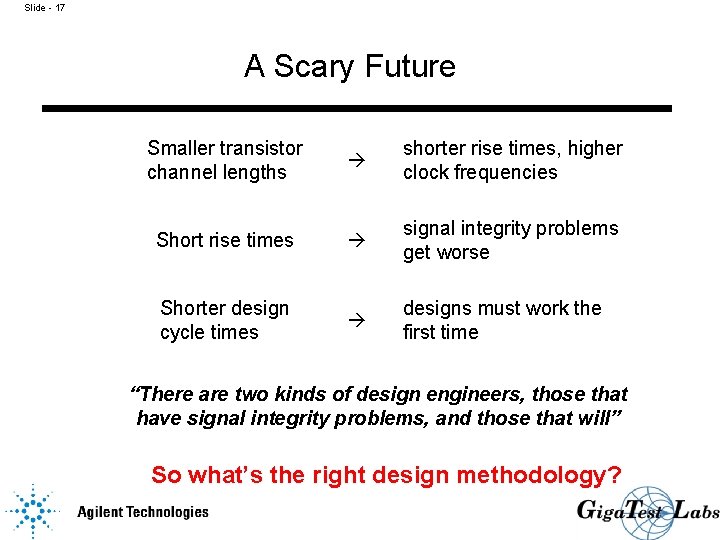
Slide - 17 A Scary Future Smaller transistor channel lengths shorter rise times, higher clock frequencies Short rise times signal integrity problems get worse Shorter design cycle times designs must work the first time “There are two kinds of design engineers, those that have signal integrity problems, and those that will” So what’s the right design methodology?

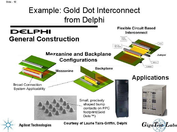
Slide - 18 Example: Gold Dot Interconnect from Delphi General Construction Applications Courtesy of Laurie Taira-Griffin, Delphi

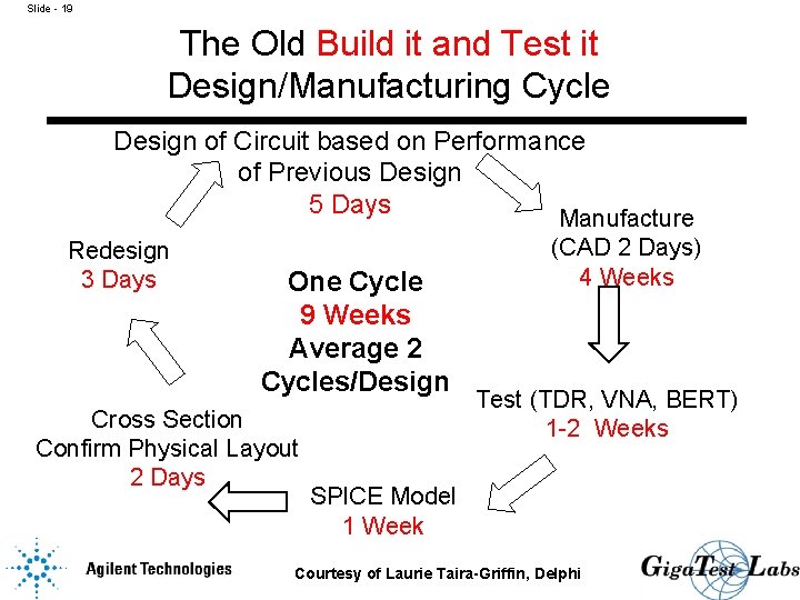
Slide - 19 The Old Build it and Test it Design/Manufacturing Cycle Design of Circuit based on Performance of Previous Design 5 Days Manufacture Redesign 3 Days One Cycle 9 Weeks Average 2 Cycles/Design Cross Section Confirm Physical Layout 2 Days (CAD 2 Days) 4 Weeks Test (TDR, VNA, BERT) 1 -2 Weeks SPICE Model 1 Week Courtesy of Laurie Taira-Griffin, Delphi

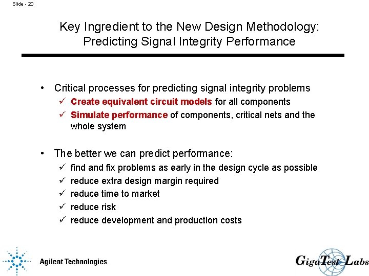
Slide - 20 Key Ingredient to the New Design Methodology: Predicting Signal Integrity Performance • Critical processes for predicting signal integrity problems ü Create equivalent circuit models for all components ü Simulate performance of components, critical nets and the whole system • The better we can predict performance: ü ü ü find and fix problems as early in the design cycle as possible reduce extra design margin required reduce time to market reduce risk reduce development and production costs

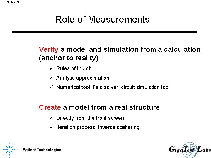
Slide - 21 Role of Measurements Verify a model and simulation from a calculation (anchor to reality) ü Rules of thumb ü Analytic approximation ü Numerical tool: field solver, circuit simulation tool Create a model from a real structure ü Directly from the front screen ü Iteration process: inverse scattering

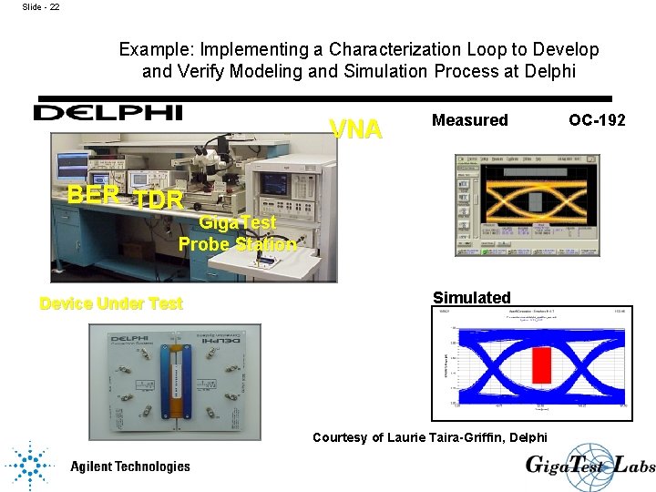
Slide - 22 Example: Implementing a Characterization Loop to Develop and Verify Modeling and Simulation Process at Delphi VNA Measured BER TDR Giga. Test Probe Station Device Under Test Simulated Courtesy of Laurie Taira-Griffin, Delphi OC-192

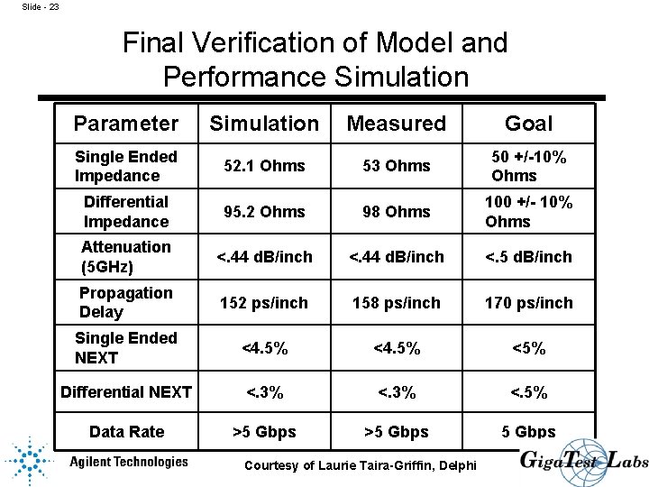
Slide - 23 Final Verification of Model and Performance Simulation Parameter Simulation Measured Goal Single Ended Impedance 52. 1 Ohms 53 Ohms 50 +/-10% Ohms Differential Impedance 95. 2 Ohms 98 Ohms 100 +/- 10% Ohms Attenuation (5 GHz) <. 44 d. B/inch <. 5 d. B/inch Propagation Delay 152 ps/inch 158 ps/inch 170 ps/inch Single Ended NEXT <4. 5% <5% Differential NEXT <. 3% <. 5% Data Rate >5 Gbps Courtesy of Laurie Taira-Griffin, Delphi

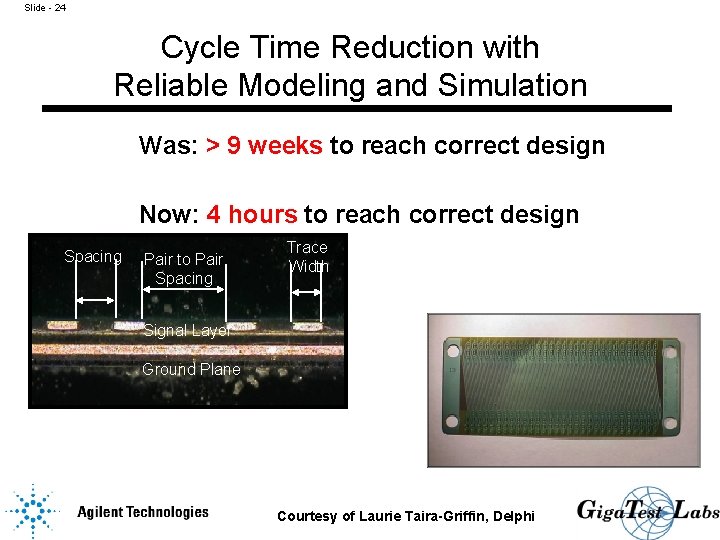
Slide - 24 Cycle Time Reduction with Reliable Modeling and Simulation Was: > 9 weeks to reach correct design Now: 4 hours to reach correct design Spacing Pair to Pair Spacing Trace Width Signal Layer Ground Plane Courtesy of Laurie Taira-Griffin, Delphi

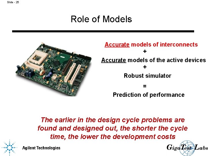
Slide - 25 Role of Models Accurate models of interconnects + Accurate models of the active devices + Robust simulator = Prediction of performance The earlier in the design cycle problems are found and designed out, the shorter the cycle time, the lower the development costs

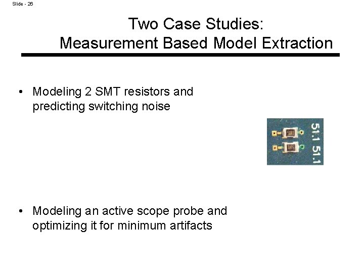
Slide - 26 Two Case Studies: Measurement Based Model Extraction • Modeling 2 SMT resistors and predicting switching noise • Modeling an active scope probe and optimizing it for minimum artifacts

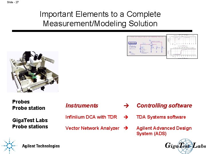
Slide - 27 Important Elements to a Complete Measurement/Modeling Solution Probes Probe station Giga. Test Labs Probe stations Instruments Controlling software Infiniium DCA with TDR TDA Systems software Vector Network Analyzer Agilent Advanced Design System (ADS)

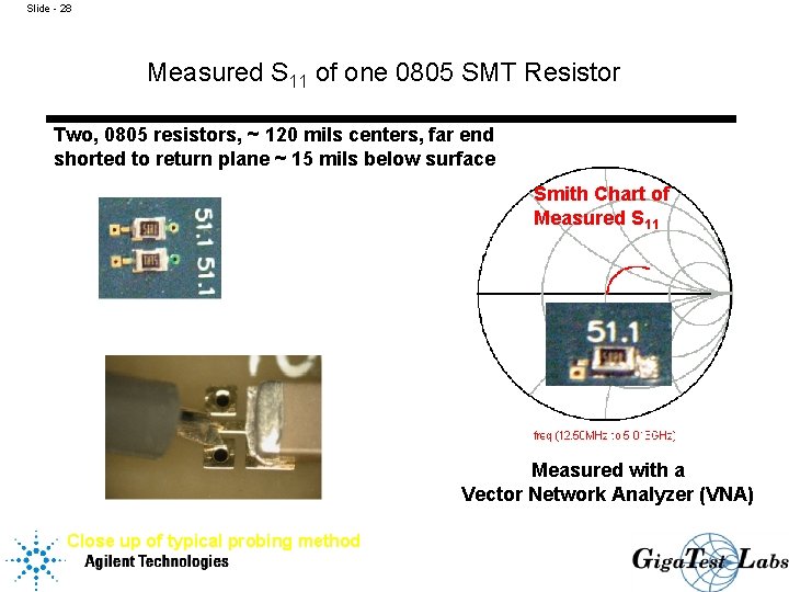
Slide - 28 Measured S 11 of one 0805 SMT Resistor Two, 0805 resistors, ~ 120 mils centers, far end shorted to return plane ~ 15 mils below surface Smith Chart of Measured S 11 Measured with a Vector Network Analyzer (VNA) Close up of typical probing method

Slide - 29 See additional Notes

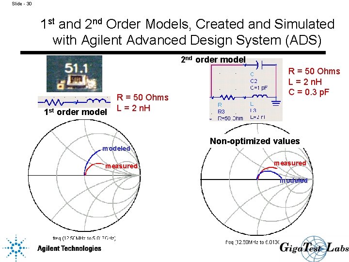
Slide - 30 1 st and 2 nd Order Models, Created and Simulated with Agilent Advanced Design System (ADS) 2 nd order model 1 st order model R = 50 Ohms L = 2 n. H modeled measured R = 50 Ohms L = 2 n. H C = 0. 3 p. F Non-optimized values measured modeled

Slide - 31 See additional Notes

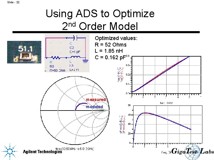
Slide - 32 Using ADS to Optimize 2 nd Order Model Optimized values: R = 52 Ohms L = 1. 85 n. H C = 0. 162 p. F measured modeled

Slide - 33 Features of the Model • A simple model matches the measured performance very well • The interconnect model is very accurate • Bandwidth of the model is at least 5 GHzcould be higher • The precise parameter values will depend on the location of the return plane and the via structures

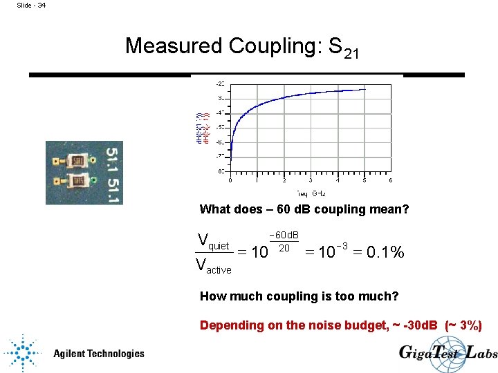
Slide - 34 Measured Coupling: S 21 What does – 60 d. B coupling mean? - 60 d. B Vquiet = 10 20 = 10 -3 = 0. 1% Vactive How much coupling is too much? Depending on the noise budget, ~ -30 d. B (~ 3%)

Slide - 35 See additional Notes

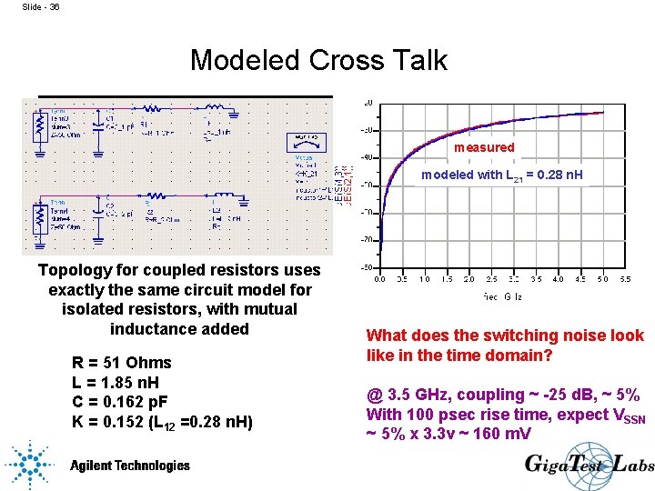
Slide - 36 Modeled Cross Talk measured modeled with L 21 = 0. 28 n. H Topology for coupled resistors uses exactly the same circuit model for isolated resistors, with mutual inductance added R = 51 Ohms L = 1. 85 n. H C = 0. 162 p. F K = 0. 152 (L 12 =0. 28 n. H) What does the switching noise look like in the time domain? @ 3. 5 GHz, coupling ~ -25 d. B, ~ 5% With 100 psec rise time, expect VSSN ~ 5% x 3. 3 v ~ 160 m. V

Slide - 37 See additional Notes

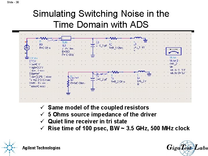
Slide - 38 Simulating Switching Noise in the Time Domain with ADS ü ü Same model of the coupled resistors 5 Ohms source impedance of the driver Quiet line receiver in tri state Rise time of 100 psec, BW ~ 3. 5 GHz, 500 MHz clock

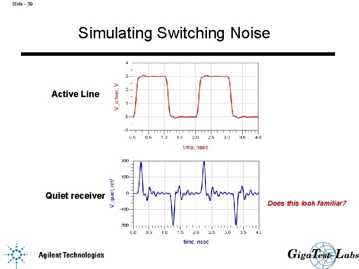
Slide - 39 Simulating Switching Noise Active Line Quiet receiver Does this look familiar?

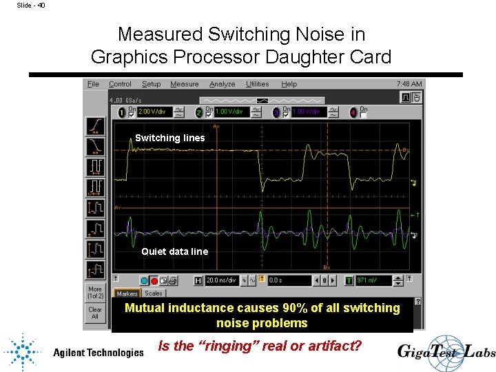
Slide - 40 Measured Switching Noise in Graphics Processor Daughter Card Switching lines Quiet data line Mutual inductance causes 90% of all switching noise problems Is the “ringing” real or artifact?

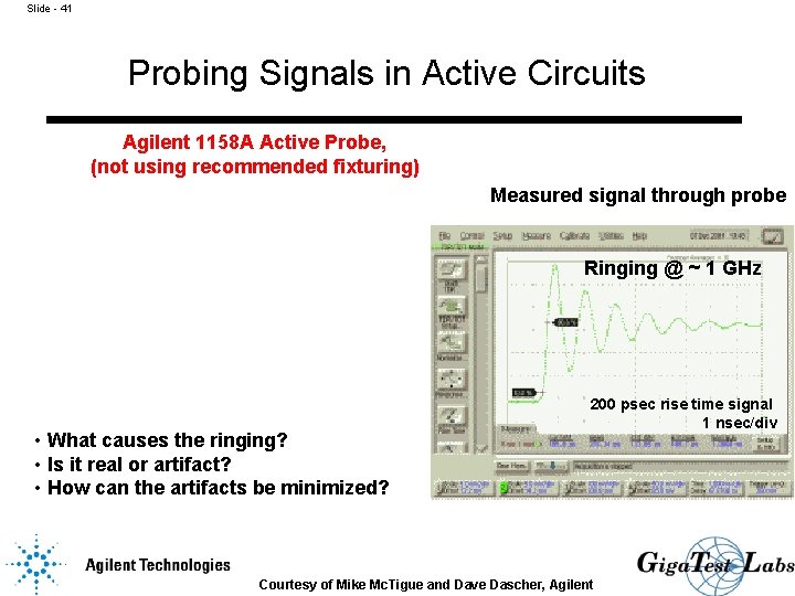
Slide - 41 Probing Signals in Active Circuits Agilent 1158 A Active Probe, (not using recommended fixturing) Measured signal through probe Ringing @ ~ 1 GHz • What causes the ringing? • Is it real or artifact? • How can the artifacts be minimized? 200 psec rise time signal 1 nsec/div Courtesy of Mike Mc. Tigue and Dave Dascher, Agilent

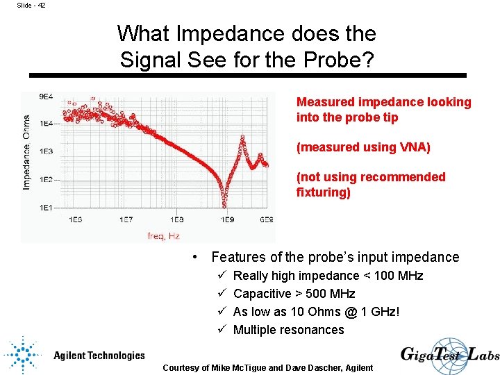
Slide - 42 What Impedance does the Signal See for the Probe? Measured impedance looking into the probe tip (measured using VNA) (not using recommended fixturing) • Features of the probe’s input impedance ü ü Really high impedance < 100 MHz Capacitive > 500 MHz As low as 10 Ohms @ 1 GHz! Multiple resonances Courtesy of Mike Mc. Tigue and Dave Dascher, Agilent

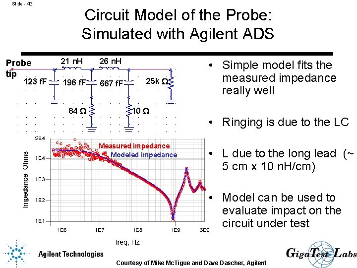
Slide - 43 Probe tip 123 f. F Circuit Model of the Probe: Simulated with Agilent ADS 21 n. H 26 n. H 196 f. F 667 f. F 84 25 k 10 Measured impedance Modeled impedance • Simple model fits the measured impedance really well • Ringing is due to the LC • L due to the long lead (~ 5 cm x 10 n. H/cm) • Model can be used to evaluate impact on the circuit under test Courtesy of Mike Mc. Tigue and Dave Dascher, Agilent

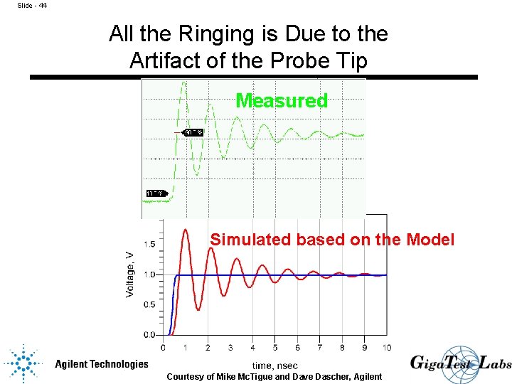
Slide - 44 All the Ringing is Due to the Artifact of the Probe Tip Measured Simulated based on the Model Courtesy of Mike Mc. Tigue and Dave Dascher, Agilent

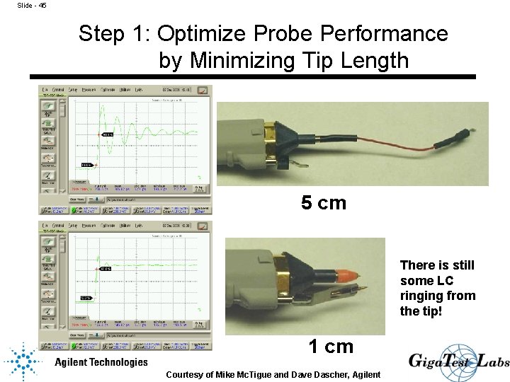
Slide - 45 Step 1: Optimize Probe Performance by Minimizing Tip Length 5 cm There is still some LC ringing from the tip! 1 cm Courtesy of Mike Mc. Tigue and Dave Dascher, Agilent

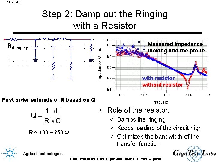
Slide - 46 Step 2: Damp out the Ringing with a Resistor Measured impedance looking into the probe Rdamping with resistor without resistor First order estimate of R based on Q ~ 1 • Role of the resistor: R ~ 100 – 250 ü Damps the ringing ü Keeps loading of the circuit high ü Optimizes the bandwidth of the transfer function Courtesy of Mike Mc. Tigue and Dave Dascher, Agilent

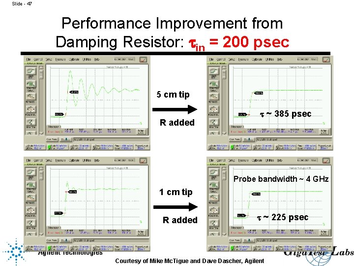
Slide - 47 Performance Improvement from Damping Resistor: tin = 200 psec 5 cm tip R added t ~ 385 psec Probe bandwidth ~ 4 GHz 1 cm tip R added t ~ 225 psec Courtesy of Mike Mc. Tigue and Dave Dascher, Agilent

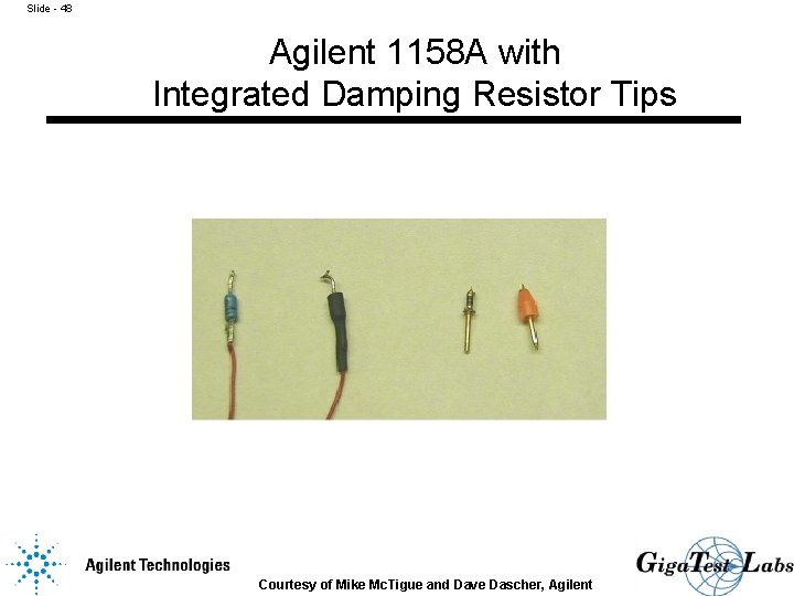
Slide - 48 Agilent 1158 A with Integrated Damping Resistor Tips Courtesy of Mike Mc. Tigue and Dave Dascher, Agilent

Slide - 49 Summary of Good Probe Techniques Agilent 1158 A 1. Keep probe lengths as short as possible 2. Use integrated damping resistor 3. Select R value based on Agilent recommended table 4. Always consider the impact of the probe’s impedance on the circuit performance Courtesy of Mike Mc. Tigue and Dave Dascher, Agilent

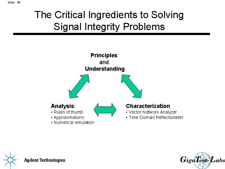
Slide - 50 The Critical Ingredients to Solving Signal Integrity Problems Principles and Understanding Analysis: Characterization • Rules of thumb • Approximations • Numerical simulation • Vector Network Analyzer • Time Domain Reflectometer

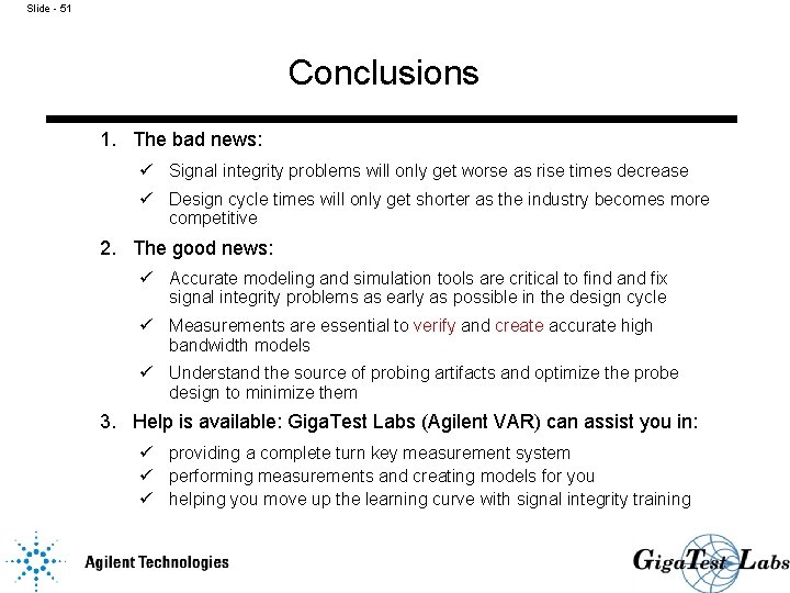
Slide - 51 Conclusions 1. The bad news: ü Signal integrity problems will only get worse as rise times decrease ü Design cycle times will only get shorter as the industry becomes more competitive 2. The good news: ü Accurate modeling and simulation tools are critical to find and fix signal integrity problems as early as possible in the design cycle ü Measurements are essential to verify and create accurate high bandwidth models ü Understand the source of probing artifacts and optimize the probe design to minimize them 3. Help is available: Giga. Test Labs (Agilent VAR) can assist you in: ü providing a complete turn key measurement system ü performing measurements and creating models for you ü helping you move up the learning curve with signal integrity training