Shift Register FSM design procedure Describe FSM behavior

Shift Register

FSM design procedure • Describe FSM behavior, e. g. state diagram – Inputs and Outputs – States (symbolic) – State transitions • State diagram to state transition table, i. e. truth table – Inputs: inputs and current state – Outputs: outputs and next state • State encoding – decide on representation of states – lots of choices • Implementation – flip-flop for each state bit – synthesize combinational logic from encoded state table

Synthesis Example • Implement simple count sequence: 000, 011, 101, 110 • Derive the state transition table from the state transition diagram 010 101 110 011 note the don't care conditions that arise from the unused state codes
 • Synthesize logic for next state functions derive input")
Don’t cares in FSMs (cont’d) • Synthesize logic for next state functions derive input equations for flip-flops

• Start-up states Self-starting FSMs – at power-up, FSM may be in an used or invalid state – design must guarantee that it (eventually) enters a valid state • Self-starting solution – design FSM so that all the invalid states eventually transition to a valid state may limit exploitation of don't cares

Self-starting FSMs Deriving state transition table from don't care assignment

Comparison of Mealy and Moore machines • Mealy machines tend to have fewer states – different outputs on arcs (i*n) rather than states (n) • Mealy machines react faster to inputs – react in same cycle – don't need to wait for clock – delay to output depends on arrival of input • Moore machines are generally safer to use – outputs change at clock edge (always one cycle later) – in Mealy machines, input change can cause output change as soon as logic is done – a big problem when two machines are interconnected – asynchronous feedback

Implementing an FSM • 1. Perform state assignment – different assignments may give very different results – no really good heuristics – using an extra bit or two for state works well • FPGAs often use a 1 -hot encoding • 2. Convert state diagram to state table – equivalent representation – mechanical • 3. State table gives truth table for next state and output functions – synthesize into logic circuit – e. g. 2 -level logic implementation

Example: Vending Machine FSM General Machine Concept: • deliver package of gum after 15 cents deposited • single coin slot for dimes, nickels • no change Step 1. Understand the problem: Draw a picture! Coin Sensor N D Reset Vending Machine FSM Open Clk Block Diagram Gum Release Mechanism

Vending Machine Example

Vending Machine Example Step 3: State Minimization Reset Present State 0¢ 0¢ N 5¢ D N 5¢ 10¢ D N, D 10¢ 15¢ [open] reuse states whenever possible 15¢ Inputs D N 0 0 0 1 1 0 0 0 1 1 X X Next State 0¢ 5¢ 10¢ X 5¢ 10¢ 15¢ X 15¢ Symbolic State Table Output Open 0 0 0 X 1

Vending Machine Example Step 4: State Encoding Present State Inputs D N Q 1 Q 0 0 0 1 1 0 1 1 0 0 1 1 Next State D 1 D 0 0 1 1 0 X X 0 1 1 X X 1 1 1 X X Output Open 0 0 0 X 1 1 1 X

Vending Machine Example

Data Converters Santanu Chattopadhyay Electronics and Electrical Communication Engineering
 • Analog-to-Digital Converters (ADCs)")
• Digital-to-Analog Converters (DACs) • Analog-to-Digital Converters (ADCs)
")
Digital-to-Analog Converter (DAC)
 converts a digital")
What is a DAC? • A digital to analog converter (DAC) converts a digital signal to an analog voltage or current output. 100101… DAC

What is a DAC?

Types of DACs • Many types of DACs available • Usually switches, resistors, and op-amps used to implement conversion • Two Types: – Binary Weighted Resistor – R-2 R Ladder

Binary Weighted Resistor • Utilizes a summing op-amp circuit • Weighted resistors are used to distinguish each bit from the most significant to the least significant • Transistors are used to switch between Vref and ground (bit high or low)

Binary Weighted Resistor • Assume Ideal Op-amp • No current into op-amp • Virtual ground at inverting input • Vout= -IRf Vref R 2 R 4 R 2 n. R I Rf + Vout

Binary Weighted Resistor Voltages V 1 through Vn are either Vref if corresponding bit is high or ground if corresponding bit is low V 1 is most significant bit Vn is least significant bit MSB LSB

Binary Weighted Resistor If Rf=R/2 For example, a 4 -Bit converter yields Where b 3 corresponds to Bit-3, b 2 to Bit-2, etc.

Binary Weighted Resistor • • Advantages – Simple Construction/Analysis – Fast Conversion Disadvantages – Requires large range of resistors (2000: 1 for 12 -bit DAC) with necessary high precision for low resistors – Requires low switch resistances in transistors – Can be expensive. Therefore, usually limited to 8 -bit resolution.

R-2 R Ladder Vref Bit: 0 Each bit corresponds to a switch: If the bit is high, the corresponding switch is connected to the inverting input of the op-amp. 0 0 0 4 -Bit Converter Vout If the bit is low, the corresponding switch is connected to ground.

R-2 R Ladder Vref V 1 V 2 V 3 Ideal Op-amp 2 R 2 R

R-2 R Ladder Vref V 1 V 2 V 3 R I Likewise, Vout R

R-2 R Ladder Vref V 1 V 2 Results: V 3 Vout Where b 3 corresponds to bit 3, b 2 to bit 2, etc. If bit n is set, bn=1 If bit n is clear, bn=0

R-2 R Ladder For a 4 -Bit R-2 R Ladder For general n-Bit R-2 R Ladder or Binary Weighted Resister DAC
")
R-2 R Ladder • Advantages – Only two resistor values (R and 2 R) – Does not require high precision resistors • Disadvantage – Lower conversion speed than binary weighted DAC

Specifications of DACs • • • Resolution Speed Linearity Settling Time Reference Voltages Errors

Resolution • Smallest analog increment corresponding to 1 LSB change • An N-bit resolution can resolve 2 N distinct analog levels • Common DAC has a 8 -16 bit resolution

Speed • Rate of conversion of a single digital input to its analog equivalent • Conversion rate depends on – clock speed of input signal – settling time of converter • When the input changes rapidly, the DAC conversion speed must be high.

Linearity • The difference between the desired analog output and the actual output over the full range of expected values

Linearity • Ideally, a DAC should produce a linear relationship between the digital input and analog output Linearity (Ideal) Non-Linearity

Settling Time • Time required for the output signal to settle within +/- ½ LSB of its final value after a given change in input scale • Limited by slew rate of output amplifier • Ideally, an instantaneous change in analog voltage would occur when a new binary word enters into DAC

Reference Voltages • Used to determine how each digital input will be assigned to each voltage division • Types: – Non-multiplier DAC: Vref is fixed – Multiplier DAC: Vref provided by external source

Types of Errors Associated with DACs • • Gain Offset Full Scale Resolution Non-Linearity Non-Monotonic Settling Time and Overshoot

Gain Error • Occurs when the slope of the actual output deviates from the ideal output

Offset Error • Occurs when there is a constant offset between the actual output and the ideal output

Full Scale Error • Occurs when the actual signal has both gain and offset errors

Resolution Error • Poor representation of ideal output due to poor resolution • Size of voltage divisions affect the resolution

Non-Linearity Error • Occurs when analog output signal is non-linear • Two Types – Differential – analog step-size changes with increasing digital input (measure of largest deviation; between successive bits) – Integral – amount of deviation from a straight line after offset and gain errors removed; on concurrent bits

Non-Linearity Error, cont.

Non-Monotonic Error • Occurs when an increase in digital input results in a decrease in the analog output

Settling Time and Overshoot Error Analog • Settling Time – time Output +1/2*VLSB required for the output Ideal to fall with in +/- ½ VLSB Output -1/2*VLSB • Overshoot – occurs when analog output Settling overshoots the ideal Time output Time

Applications • • • Digital Motor Control Computer Printers Sound Equipment (e. g. CD/MP 3 Players, etc. ) Electronic Cruise Control Digital Thermostat
")
Analog-to-Digital Converter (ADC)

Background Information • • What is ADC? Conversion Process Accuracy Examples of ADC applications

Signal Types Analog Signals • Any continuous signal, that is a time varying variable of the signal, is a representation of some other time varying quantity – Measures one quantity in terms of some other quantity – Examples • Speedometer needle as function of speed • Radio volume as function of knob movement t

Signal Types Digital Signals • Consist of only two states – Binary States – On and off • Computers can only perform processing on digitized signals 1 0
 • An electronic integrated circuit which converts a signal from analog")
Analog-Digital Converter (ADC) • An electronic integrated circuit which converts a signal from analog (continuous) to digital (discrete) form • Provides a link between the analog world of transducers and the digital world of signal processing and data handling t

ADC Conversion Process Two main steps of process 1. Sampling and Holding 2. Quantization and Encoding

Sampling & Hold ADC Process • Measuring analog signals at uniform time intervals – Ideally twice as fast as what we are sampling • Digital system works with discrete states – Taking samples from each location • Reflects sampled and hold signal – Digital approximation

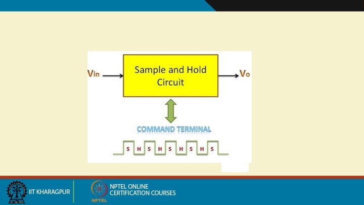
Sample and Hold Circuit • The time during which sample and hold circuit generates the sample of the input signal is called sampling time. • Similarly, the time duration of the circuit during which it holds the sampled value is called holding time. • Sampling time is generally between 1µs to 14 µs while the holding time can assume any value as required in the application. • Capacitor is the heart of sample and hold circuit. The capacitor charges to its peak value when the switch is closed, i. e. during sampling and holds the sampled voltage when the switch is open.

Circuit Diagram

Circuit Diagram

• • • The N-channel Enhancement MOSFET is used as the switching element. Input voltage is applied through its drain terminal and control voltage to its gate terminal. When the positive pulse of the control voltage is applied, the MOSFET will be switched to ON state - it acts as a closed switch. On the contrary, when the control voltage is zero then the MOSFET will be switched to OFF state - acts as an open switch. When the switch is closed, the analog signal applied to it through the drain terminal is fed to the capacitor. The capacitor charges to its peak value. When the MOSFET switch is opened, then the capacitor stops charging. Due to the high impedance operational amplifier connected at the end of the circuit, the capacitor experiences high impedance due to this it cannot get discharged. Charge is held by the capacitor for a definite amount of time - holding period. Time in which samples of the input voltage is generated - sampling period.

Input-Output Waveform

LF 398

Applications of Sample and Hold Circuit • • • Data Distribution System Sampling Oscilloscopes Data Conversion System Digital Voltmeters Analog Signal Processing Signal Constructional Filters

ADC Process Quantizing • Separating the input signal into discrete states with K increments • K=2 N – N is the number of bits of the ADC • Analog quantization size – Q=(Vmax-Vmin)/2 N – Q is the Resolution Encoding • Assigning a unique digital code to each state for input into the microprocessor

ADC Process Quantization & Coding • Use original analog signal

ADC Process Quantization & Coding • Use original analog signal • Apply 2 bit coding 11 10 01 00 K=22 00 01 10 11

ADC Process Quantization & Coding • Use original analog signal • Apply 2 bit coding 11 10 01 00 K=22 00 01 10 11

ADC Process Quantization & Coding • Use original analog signal • Apply 3 bit coding

ADC Process Quantization & Coding • Use original analog signal • Apply 3 bit coding • Better representation of input information with additional bits • MCS 12 has max of 10 bits

ADC Process-Accuracy The accuracy of an ADC can be improved by increasing: Sampling Rate, Ts • • Based on number of steps required in the conversion process Increases the maximum frequency that can be measured t Resolution (bit depth), Q • Improves accuracy in measuring amplitude of analog signal t
 – Occurs when the input signal is changing much")
ADC-Error Possibilities • Aliasing (sampling) – Occurs when the input signal is changing much faster than the sample rate – Should follow the Nyquist Rule when sampling • Answers question of what sample rate is required • Use a sampling frequency at least twice as high as the maximum frequency in the signal to avoid aliasing • fsample>2*fsignal • Quantization Error (resolution) – Optimize resolution – Dependent on ADC converter of microcontoller

ADC Applications • ADC are used virtually everywhere an analog signal has to be processed, stored, or transported in digital form – Microphones – Strain Gages – Thermocouple – Digital Multimeters

Types of ADC • Successive Approximation A/D Converter • Flash A/D Converter • Dual Slope A/D Converter

Successive Approximation ADC § Elements • • DAC = Digital to Analog Converter EOC = End of Conversion SAR = Successive Approximation Register S/H = Sample and Hold Circuit Vin = Input Voltage Comparator Vref = Reference Voltage

Successive Approximation ADC § Algorithm • • Uses an N-bit DAC and original analog results Performs a binary comparison of VDAC and Vin MSB is initialized at 1 for DAC If Vin < VDAC (VREF / 2^(N=1)) then MSB is reset to 0 If Vin > VDAC (VREF / 2^(N+1)) successive bit is set to 1 Algorithm is repeated up to LSB At end DAC in = ADC out N-bit conversion requires N comparison cycles

Successive Approximation ADC - Example

Flash ADC § Also known as parallel ADC § Elements • Encoder – Converts output of comparators to binary • Comparators

• Flash ADC

Flash ADC Example Vin = 5. 5 V, Vref= 8 V Vin lies in between Vcomp 5 & Vcomp 6 Vcomp 5 = Vref*5/8 = 5 V Vcomp 6 = Vref*6/8 = 6 V Comparator 1 - 5 => output 1 Comparator 6 - 7 => output 0 Encoder Octal Input = sum(0011111) = 5 Encoder Binary Output = 1 0 1

Dual Slope A/D Converter • Also known as an Integrating ADC

Dual-Slope ADC – How It Works • • • An unknown input voltage is applied to the input of the integrator and allowed to ramp for a fixed time period (tu) Then, a known reference voltage of opposite polarity is applied to the integrator and is allowed to ramp until the integrator output returns to zero (td) The input voltage is computed as a function of the reference voltage, the constant run-up time period, and the measured run-down time period The run-down time measurement is usually made in units of the converter's clock, so longer integration times allow for higher resolutions The speed of the converter can be improved by sacrificing resolution
 Cost (relative) Resolution (bits) Dual Slope Slow Med")
Comparison of ADC’s Type Speed (relative) Cost (relative) Resolution (bits) Dual Slope Slow Med 12 -16 Flash Very Fast High 4 -12 Successive Approx Medium – Fast Low 8 -16
- Slides: 82