Register Cell Design Page Large System architecture Large
- Slides: 19

Register Cell Design Page

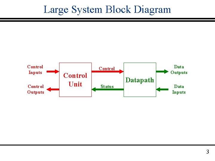
Large System architecture · Large digital systems typically partitioned into: § Datapath w Many registers, lots of Combinational Logic w Moves / processes system data w Operation specified by control word (from CU) § Control Unit w Many states and inputs w Specifies what DP does next w Decisions made based on DP status information 2

Large System Block Diagram Control Inputs Control Outputs Data Outputs Control Unit Status Datapath Data Inputs 3

Register Transfer · The movement of data stored in registers and the processing performed on the data are referred to as Register Transfer Operations · Register Transfer Language (RTL) captures register transfers and it’s components of: § The registers within the system § The operations performed on system data § The control that defines the sequence of operations 4

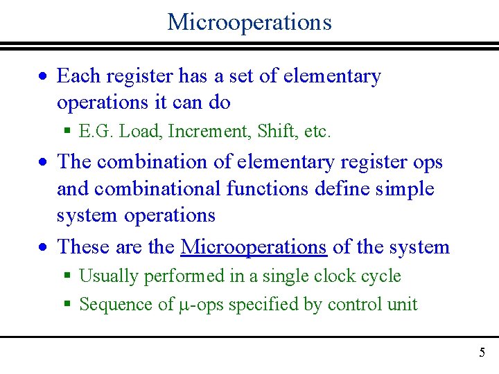
Microoperations · Each register has a set of elementary operations it can do § E. G. Load, Increment, Shift, etc. · The combination of elementary register ops and combinational functions define simple system operations · These are the Microoperations of the system § Usually performed in a single clock cycle § Sequence of -ops specified by control unit 5

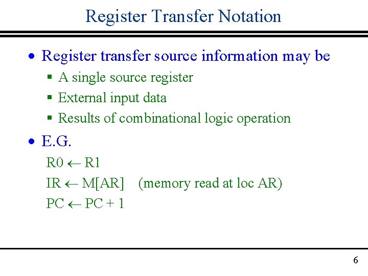
Register Transfer Notation · Register transfer source information may be § A single source register § External input data § Results of combinational logic operation · E. G. R 0 R 1 IR M[AR] (memory read at loc AR) PC + 1 6

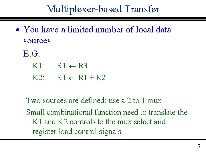
Multiplexer-based Transfer · You have a limited number of local data sources E. G. K 1: K 2: R 1 R 3 R 1 + R 2 Two sources are defined; use a 2 to 1 mux Small combinational function need to translate the K 1 and K 2 controls to the mux select and register load control signals 7

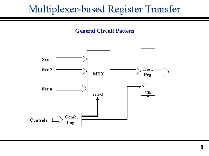
Multiplexer-based Register Transfer General Circuit Pattern Src 1 Src 2 MUX Src n select Controls Dest. Reg. EN Clk Comb. Logic 8

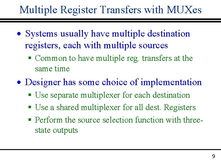
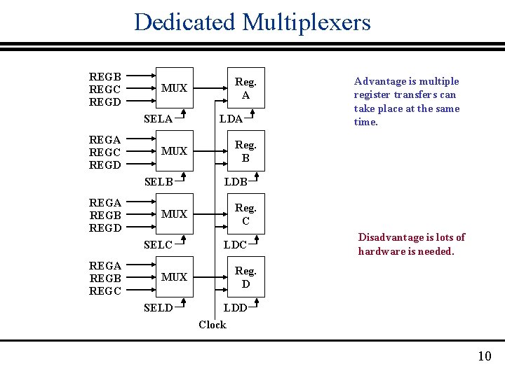
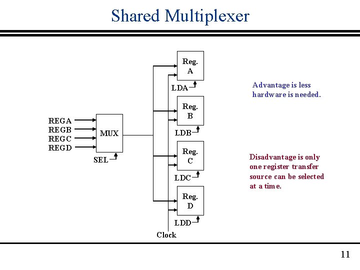
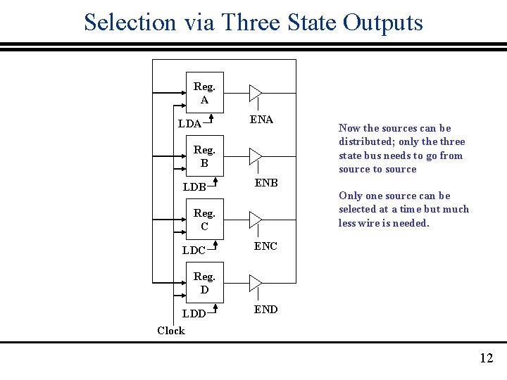
Multiple Register Transfers with MUXes · Systems usually have multiple destination registers, each with multiple sources § Common to have multiple reg. transfers at the same time · Designer has some choice of implementation § Use separate multiplexer for each destination § Use a shared multiplexer for all dest. Registers § Perform the source selection function with threestate outputs 9

Dedicated Multiplexers REGB REGC REGD MUX SELA REGC REGD MUX SELB REGA REGB REGD MUX SELC REGA REGB REGC MUX SELD Reg. A LDA Advantage is multiple register transfers can take place at the same time. Reg. B LDB Reg. C LDC Disadvantage is lots of hardware is needed. Reg. D LDD Clock 10

Shared Multiplexer Reg. A LDA REGB REGC REGD Advantage is less hardware is needed. Reg. B MUX SEL LDB Reg. C LDC Disadvantage is only one register transfer source can be selected at a time. Reg. D LDD Clock 11

Selection via Three State Outputs Reg. A LDA ENA Reg. B LDB ENB Only one source can be selected at a time but much less wire is needed. Reg. C LDC Now the sources can be distributed; only the three state bus needs to go from source to source ENC Reg. D LDD Clock END 12

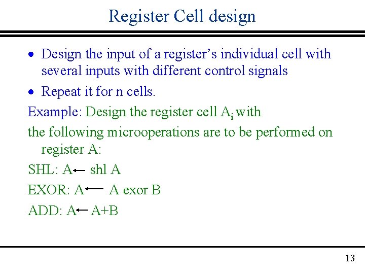
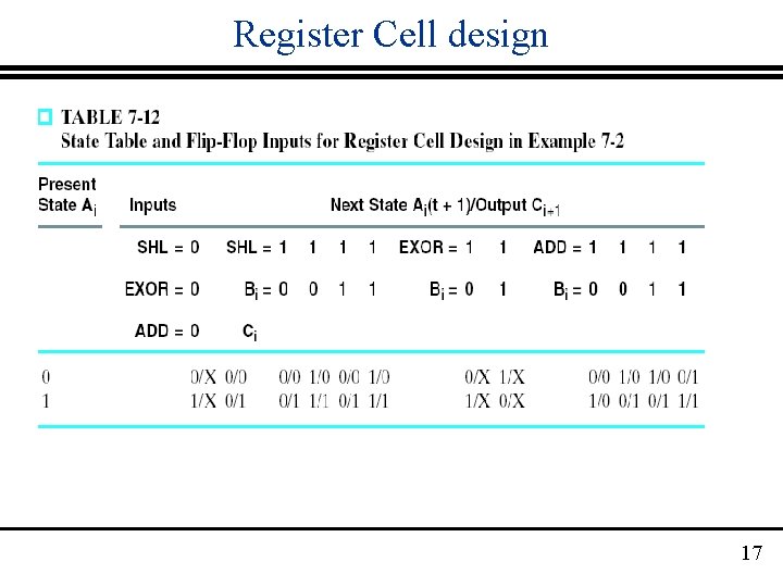
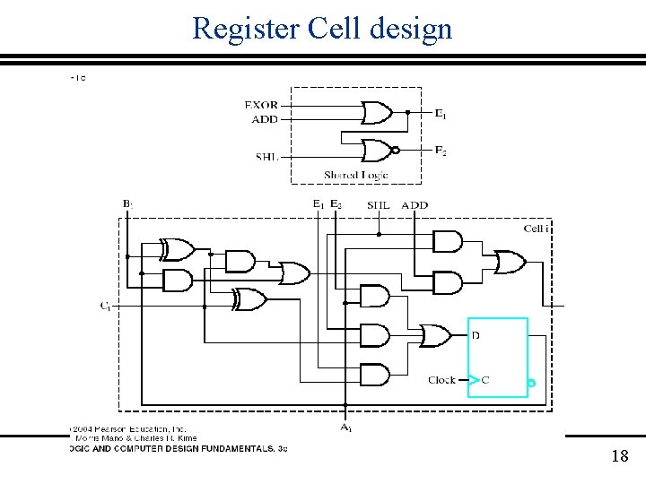
Register Cell design · Design the input of a register’s individual cell with several inputs with different control signals · Repeat it for n cells. Example: Design the register cell Ai with the following microoperations are to be performed on register A: SHL: A shl A EXOR: A A exor B ADD: A A+B 13

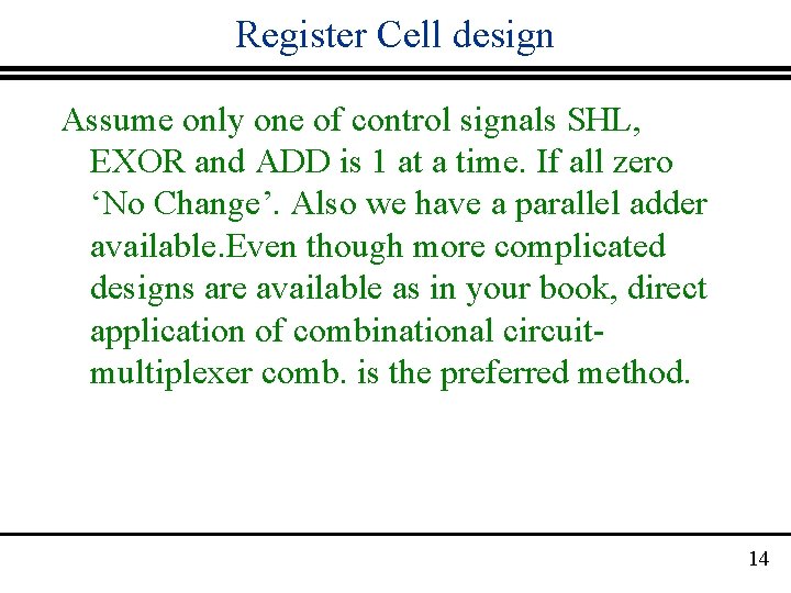
Register Cell design Assume only one of control signals SHL, EXOR and ADD is 1 at a time. If all zero ‘No Change’. Also we have a parallel adder available. Even though more complicated designs are available as in your book, direct application of combinational circuitmultiplexer comb. is the preferred method. 14

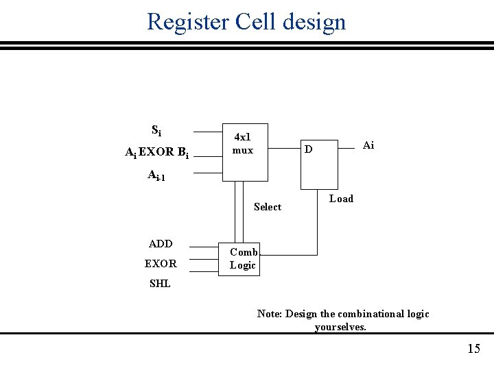
Register Cell design Si Ai EXOR Bi 4 x 1 mux Ai D Ai-1 Select ADD EXOR Load Comb. Logic SHL Note: Design the combinational logic yourselves. 15

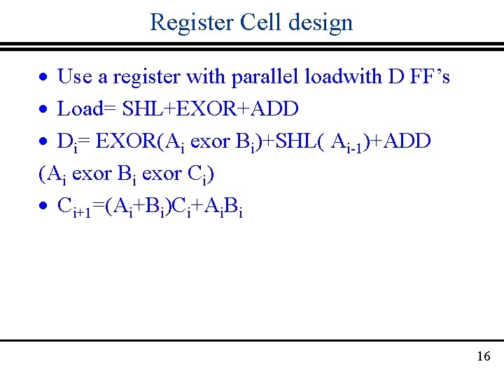
Register Cell design · Use a register with parallel loadwith D FF’s · Load= SHL+EXOR+ADD · Di= EXOR(Ai exor Bi)+SHL( Ai-1)+ADD (Ai exor Bi exor Ci) · Ci+1=(Ai+Bi)Ci+Ai. Bi 16

Register Cell design 17

Register Cell design 18

19