FlipFlop Applications Digital Electronics 2014 Project Lead The

- Slides: 19

Flip-Flop Applications Digital Electronics © 2014 Project Lead The Way, Inc.

Flip-Flop Applications This presentation will provide an overview of the following flip-flop applications: • Event Detect • Data Synchronizer • Shift Register • Frequency Divider Additional flip-flop applications will be covered in future lessons: • Asynchronous {Ripple} Counters • Synchronous {Parallel} Counters • State Machines 2

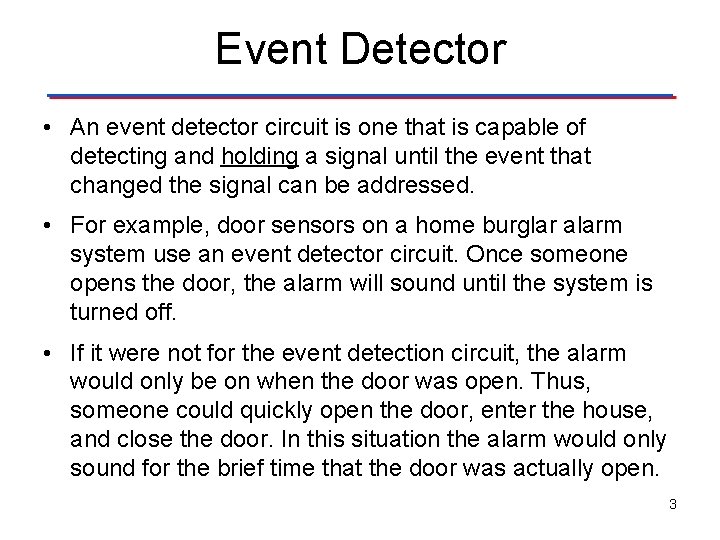
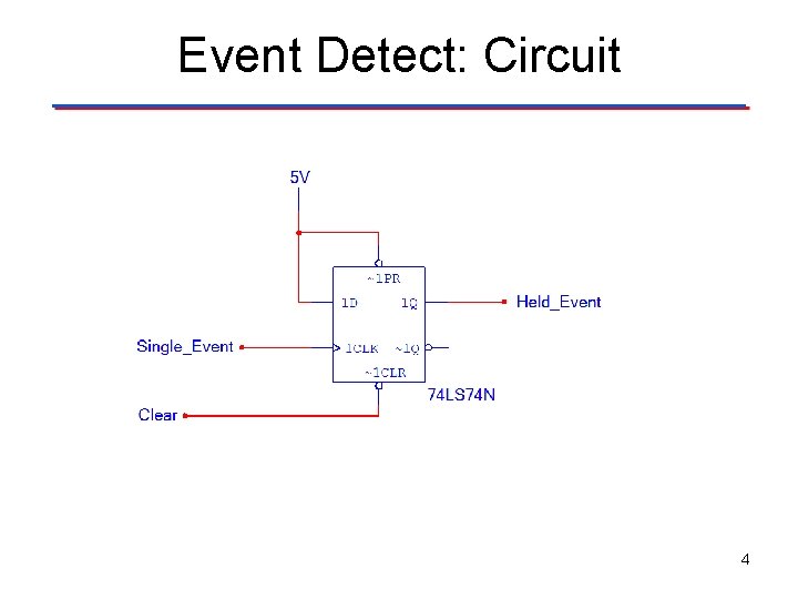
Event Detector • An event detector circuit is one that is capable of detecting and holding a signal until the event that changed the signal can be addressed. • For example, door sensors on a home burglar alarm system use an event detector circuit. Once someone opens the door, the alarm will sound until the system is turned off. • If it were not for the event detection circuit, the alarm would only be on when the door was open. Thus, someone could quickly open the door, enter the house, and close the door. In this situation the alarm would only sound for the brief time that the door was actually open. 3

Event Detect: Circuit 4

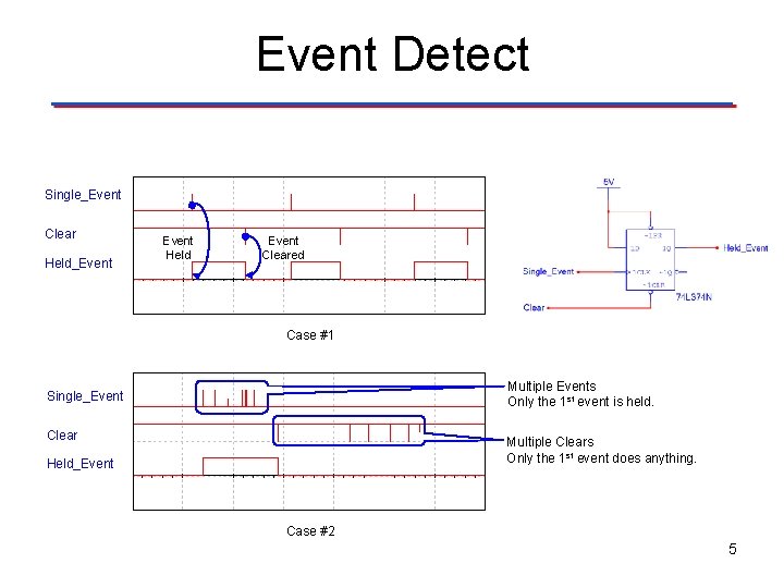
Event Detect Single_Event Clear Held_Event Held Event Cleared Case #1 Multiple Events Only the 1 st event is held. Single_Event Clear Multiple Clears Only the 1 st event does anything. Held_Event Case #2 5

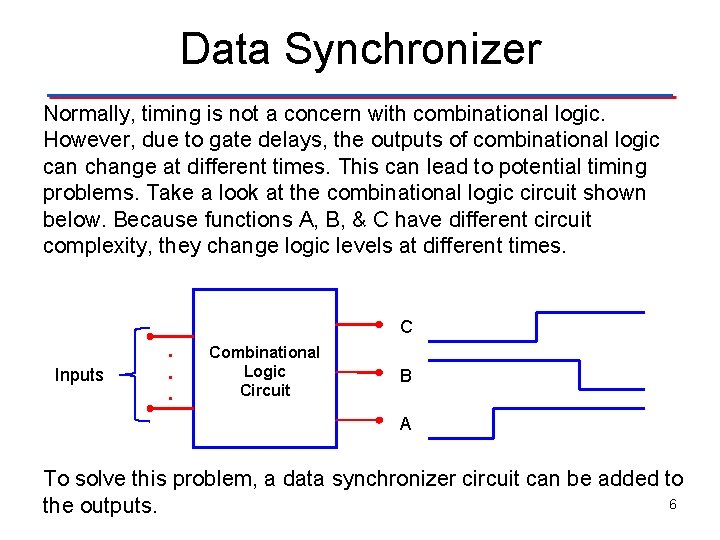
Data Synchronizer Normally, timing is not a concern with combinational logic. However, due to gate delays, the outputs of combinational logic can change at different times. This can lead to potential timing problems. Take a look at the combinational logic circuit shown below. Because functions A, B, & C have different circuit complexity, they change logic levels at different times. C Inputs . . . Combinational Logic Circuit B A To solve this problem, a data synchronizer circuit can be added to 6 the outputs.

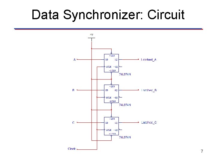
Data Synchronizer: Circuit 7

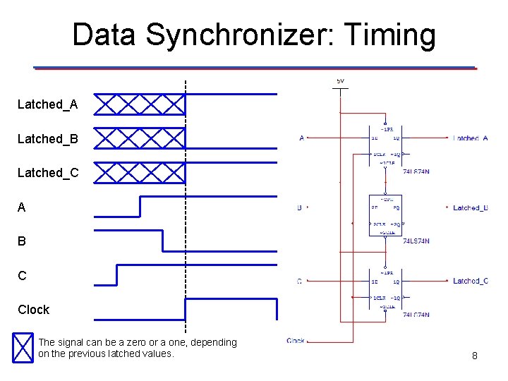
Data Synchronizer: Timing Latched_A Latched_B Latched_C A B C Clock The signal can be a zero or a one, depending on the previous latched values. 8

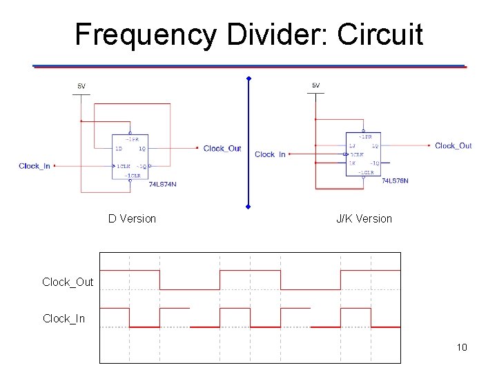
Frequency Divider • As the name implies, a frequency divider is a circuit the produces a digital output signal that is half the frequency of the input. • The frequency divider is used extensively in the design of asynchronous counters. 9

Frequency Divider: Circuit D Version J/K Version Clock_Out Clock_In 10

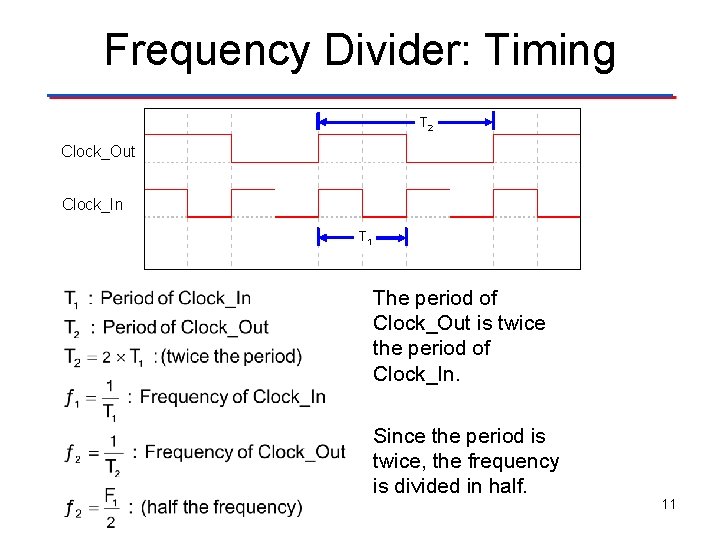
Frequency Divider: Timing T 2 Clock_Out Clock_In T 1 The period of Clock_Out is twice the period of Clock_In. Since the period is twice, the frequency is divided in half. 11

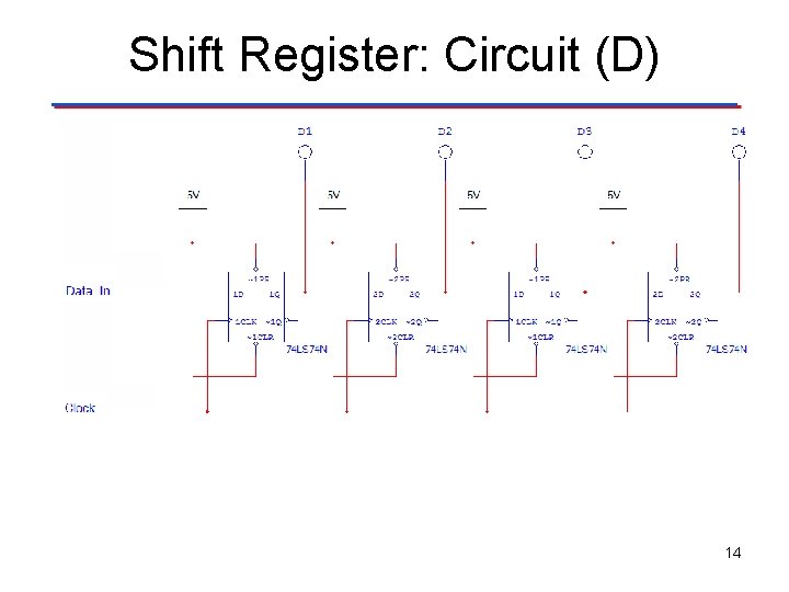
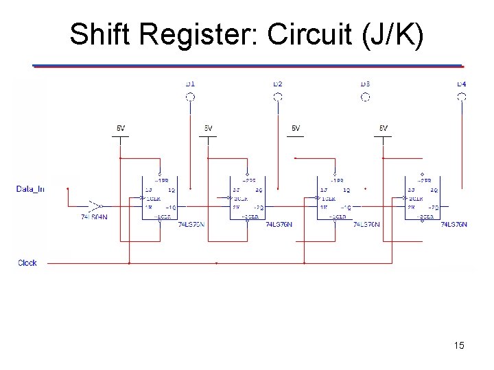
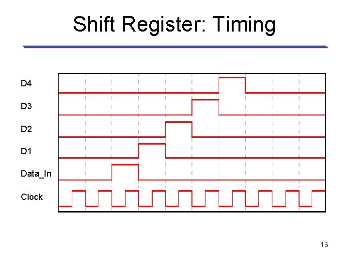
Shift Register • A shift register is a group of flip-flops (typically 4 or 8) that are arranged so that the values stored in the flip-flops are shifted from one flip-flop to the next for every clock. • Shift registers are used extensively in logic circuits to control digital displays. • A classic example is numbers being typed into a calculator. As the numbers are entered, the digits shift to the left one position. This shifting is controlled by a shift register. 12

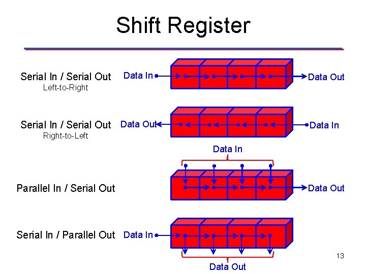
Shift Register Serial In / Serial Out Data In Data Out Left-to-Right Serial In / Serial Out Data In Right-to-Left Data In Parallel In / Serial Out Data Out Serial In / Parallel Out Data In 13 Data Out

Shift Register: Circuit (D) 14

Shift Register: Circuit (J/K) 15

Shift Register: Timing D 4 D 3 D 2 D 1 Data_In Clock 16

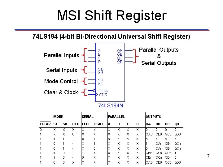
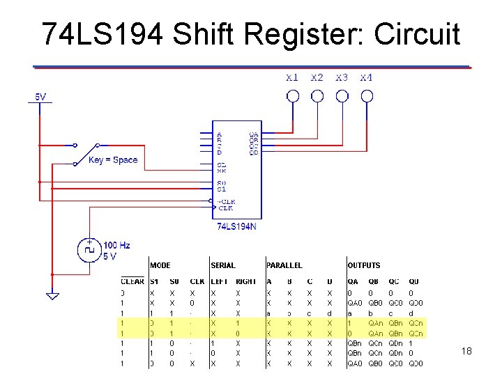
MSI Shift Register 74 LS 194 (4 -bit Bi-Directional Universal Shift Register) Parallel Inputs Parallel Outputs & Serial Outputs Serial Inputs Mode Control Clear & Clock 17

74 LS 194 Shift Register: Circuit 18

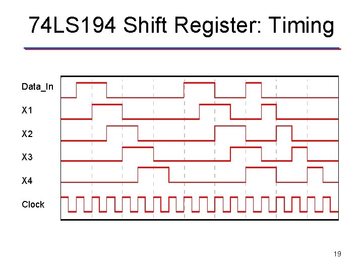
74 LS 194 Shift Register: Timing Data_In X 1 X 2 X 3 X 4 Clock 19