Rayat Shikshan Sansthas S M Joshi College Hadapsar028



- Slides: 115

Rayat Shikshan Sanstha’s S. M. Joshi College Hadapsar-028 Department of Electronics Science Integrated Circuit Logic Families Presented by. Dr. Bhalerao S. P

� Selected areas covered in this chapter: Digital IC terminology as in manufacturer data sheets. Characteristics of various TTL series. Characteristics of the various CMOS series. Major characteristics & differences among TTL, ECL, MOS, and CMOS logic families. ◦ Considerations when interfacing digital circuits from different logic families. ◦ Using voltage comparators to allow a digital system to be controlled by analog signals. ◦ Using a logic pulser and a logic probe as digital circuit troubleshooting tools. ◦ ◦

� Digital IC technology has advanced rapidly from integrations which can 1 million or more gates. � ICs pack more circuitry in a small package, so overall size of almost any system is reduced. ◦ Cost is reduced because of the economies of mass-producing large volumes of similar devices. � ICs have made digital systems more reliable by reducing the number of external interconnections from one device to another. ◦ Protected from poor soldering, breaks or shorts in connecting paths on a circuit board, and other physical problems.

� ICs cannot handle very large currents or voltage. ◦ Heat generated in such small spaces would cause temperatures to rise beyond acceptable limits. �For higher power levels, an interfacing circuit will be needed—typically of components or special power ICs. � ICs can’t easily implement certain devices such as inductors, transformers, and large capacitors. ◦ Principally used to perform low-power circuit operations—commonly called information processing.

Chapter 8 � Various logic families differ in major components in their circuitry. ◦ TTL and ECL use bipolar transistors as their major circuit element. ◦ PMOS, NMOS, and CMOS use unipolar MOSFET transistors.

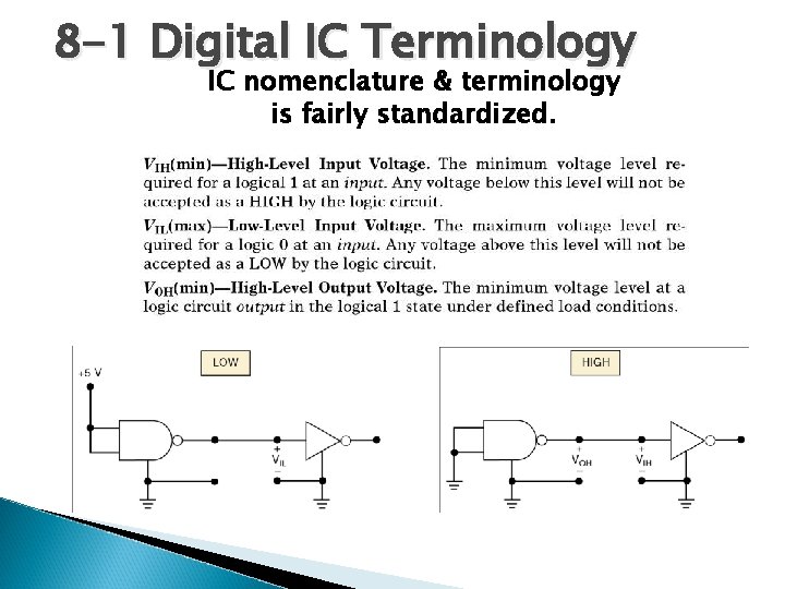
8 -1 Digital IC Terminology IC nomenclature & terminology is fairly standardized.

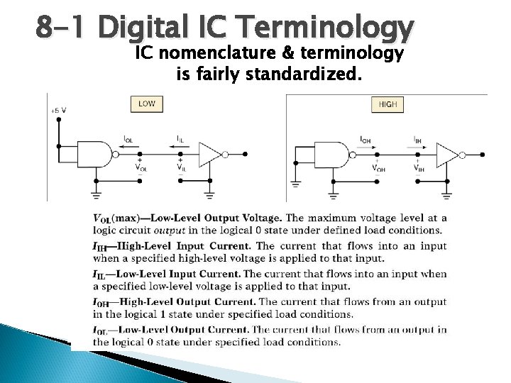
8 -1 Digital IC Terminology IC nomenclature & terminology is fairly standardized.

8 -1 Digital IC Terminology – Fan Out � A logic-circuit output is generally required to drive several logic inputs. ◦ Sometimes all ICs are from the same logic family. �But many systems have a mix of various logic families. ◦ The fan-out—loading factor—is the maximum number of logic inputs an output can drive reliably.

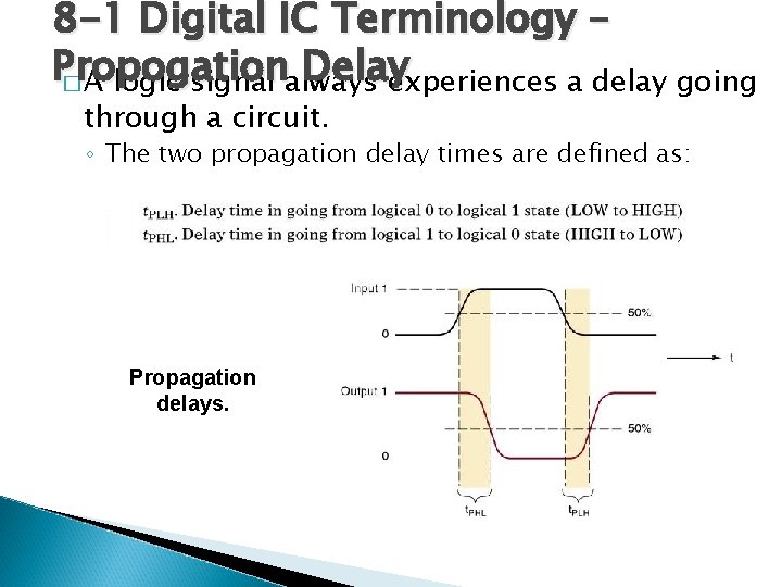
8 -1 Digital IC Terminology – Propogation Delay � A logic signal always experiences a delay going through a circuit. ◦ The two propagation delay times are defined as: Propagation delays.

8 -1 Digital IC Terminology – Power Requirements � Every IC requires a certain amount of electrical power to operate. ◦ Supplied by one or more power-supply voltages connected at VCC (TTL) or VDD (MOS devices). ◦ For many ICs, current drawn from the supply varies depending on logic states of the circuits on the chip.

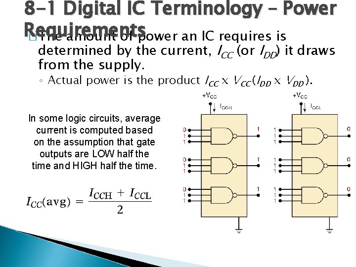
8 -1 Digital IC Terminology – Power Requirements � The amount of power an IC requires is determined by the current, ICC (or IDD) it draws from the supply. ◦ Actual power is the product ICC x VCC (IDD x VDD ). In some logic circuits, average current is computed based on the assumption that gate outputs are LOW half the time and HIGH half the time.

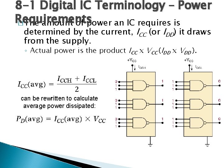
8 -1 Digital IC Terminology – Power Requirements � The amount of power an IC requires is determined by the current, ICC (or IDD) it draws from the supply. ◦ Actual power is the product ICC x VCC (IDD x VDD ). can be rewritten to calculate average power dissipated:

8 -1 Digital IC Terminology – Noise � Stray electric/magnetic fields can induce voltages on the connecting wires between logic circuits ◦ Called noise, these unwanted, spurious signals can sometimes cause unpredictable operation.

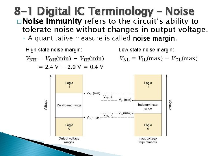
8 -1 Digital IC Terminology – Noise � Noise immunity refers to the circuit’s ability to tolerate noise without changes in output voltage. ◦ A quantitative measure is called noise margin. High-state noise margin: Low-state noise margin:

8 -1 Digital IC Terminology – Invalid Voltage � For properation, logic circuit input voltage levels must be kept out of the indeterminate range. ◦ Lower than VIL(max) or higher than VIH (min). � It �Invalid voltage will produce unpredictable output. is important to know valid voltage ranges for the logic family being used so invalid conditions can be recognized when testing or troubleshooting. � Logic families can be described by how current flows between the output of one logic circuit and the input of another.

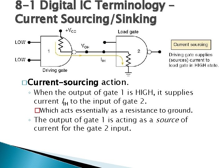
8 -1 Digital IC Terminology – Current Sourcing/Sinking � Current-sourcing action. ◦ When the output of gate 1 is HIGH, it supplies current IIH to the input of gate 2. �Which acts essentially as a resistance to ground. ◦ The output of gate 1 is acting as a source of current for the gate 2 input.

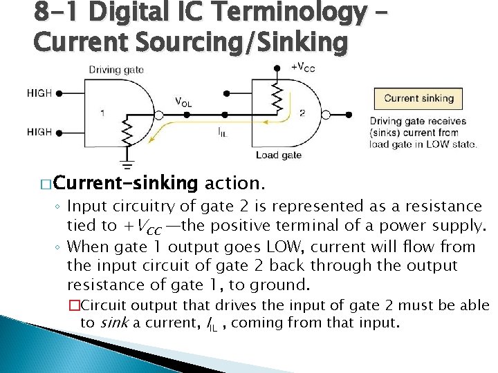
8 -1 Digital IC Terminology – Current Sourcing/Sinking � Current-sinking action. ◦ Input circuitry of gate 2 is represented as a resistance tied to +VCC —the positive terminal of a power supply. ◦ When gate 1 output goes LOW, current will flow from the input circuit of gate 2 back through the output resistance of gate 1, to ground. �Circuit output that drives the input of gate 2 must be able to sink a current, IIL , coming from that input.

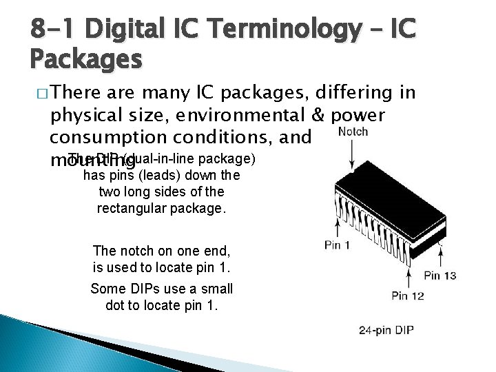
8 -1 Digital IC Terminology – IC Packages � There are many IC packages, differing in physical size, environmental & power consumption conditions, and circuit board The DIP (dual-in-line package) mounting has pins (leads) down the two long sides of the rectangular package. The notch on one end, is used to locate pin 1. Some DIPs use a small dot to locate pin 1.

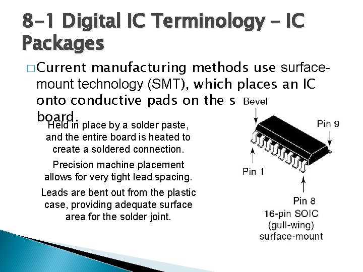
8 -1 Digital IC Terminology – IC Packages � Current manufacturing methods use surfacemount technology (SMT), which places an IC onto conductive pads on the surface of the board. Held in place by a solder paste, and the entire board is heated to create a soldered connection. Precision machine placement allows for very tight lead spacing. Leads are bent out from the plastic case, providing adequate surface area for the solder joint.

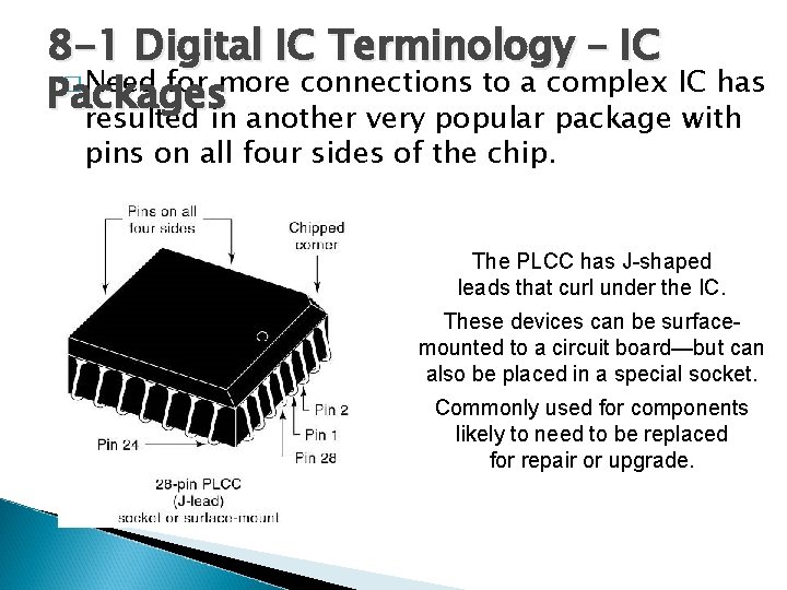
8 -1 Digital IC Terminology – IC � Need for more connections to a complex IC has Packages resulted in another very popular package with pins on all four sides of the chip. The PLCC has J-shaped leads that curl under the IC. These devices can be surfacemounted to a circuit board—but can also be placed in a special socket. Commonly used for components likely to need to be replaced for repair or upgrade.

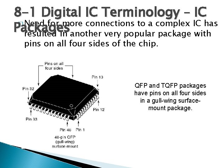
8 -1 Digital IC Terminology – IC � Need for more connections to a complex IC has Packages resulted in another very popular package with pins on all four sides of the chip. QFP and TQFP packages have pins on all four sides in a gull-wing surfacemount package.

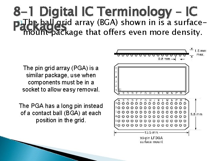
8 -1 Digital IC Terminology – IC � The ball grid array (BGA) shown in is a surface. Packages mount package that offers even more density. The pin grid array (PGA) is a similar package, use when components must be in a socket to allow easy removal. The PGA has a long pin instead of a contact ball (BGA) at each position in the grid.

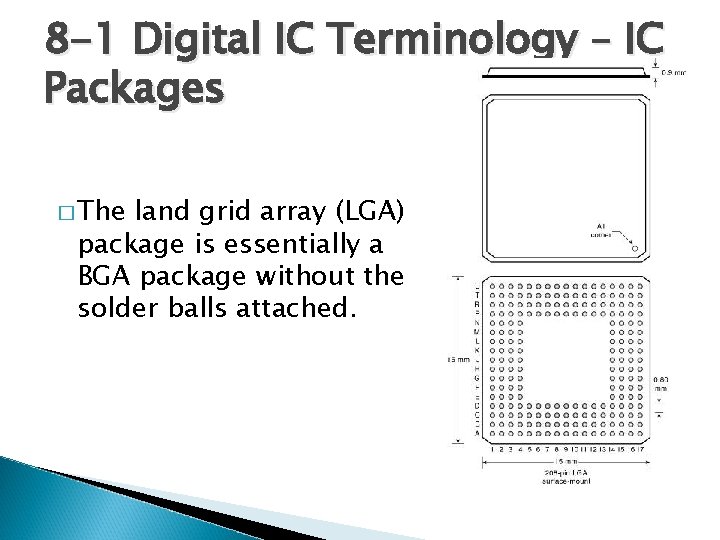
8 -1 Digital IC Terminology – IC Packages � The land grid array (LGA) package is essentially a BGA package without the solder balls attached.

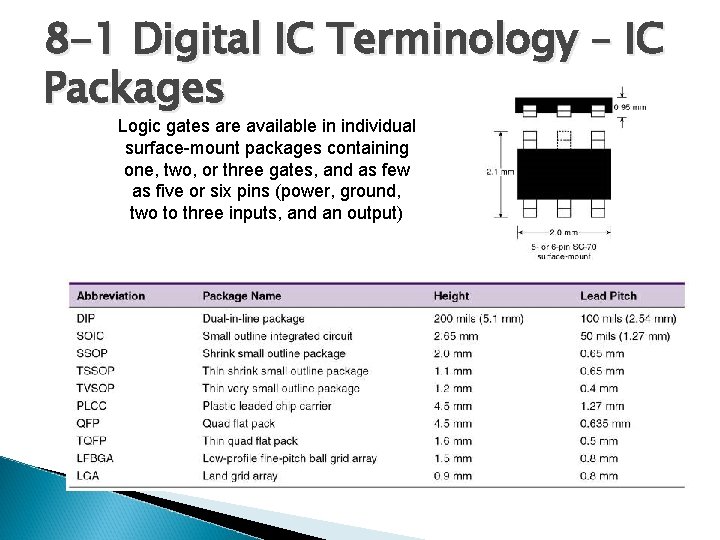
8 -1 Digital IC Terminology – IC Packages Logic gates are available in individual surface-mount packages containing one, two, or three gates, and as few as five or six pins (power, ground, two to three inputs, and an output)

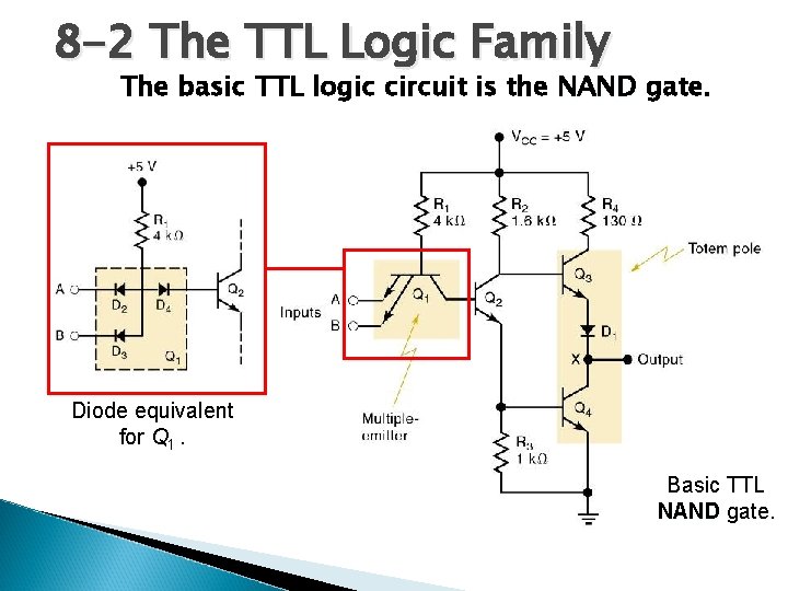
8 -2 The TTL Logic Family � Most TTL circuits have a similar structure ◦ NAND and AND gates use multiple-emitter transistor or multiple diode junction inputs. ◦ NOR and OR gates use separate input transistors. � The input will be the cathode of a P-N junction ◦ A HIGH input will turn off the junction. �Only a leakage current is generated. ◦ A LOW input turns on the junction. �Relatively large current is generated. � Most TTL circuits have some type of totempole output configuration.

8 -2 The TTL Logic Family The basic TTL logic circuit is the NAND gate. Diode equivalent for Q 1. Basic TTL NAND gate.

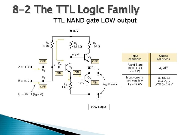
8 -2 The TTL Logic Family TTL NAND gate LOW output

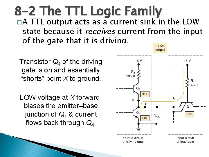
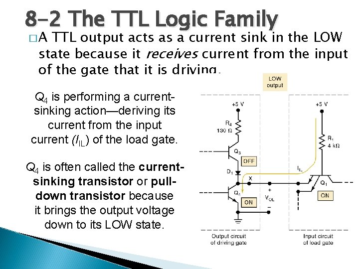
8 -2 The TTL Logic Family �A TTL output acts as a current sink in the LOW state because it receives current from the input of the gate that it is driving. Transistor Q 4 of the driving gate is on and essentially “shorts” point X to ground. LOW voltage at X forwardbiases the emitter–base junction of Q 1 & current flows back through Q 4.

8 -2 The TTL Logic Family �A TTL output acts as a current sink in the LOW state because it receives current from the input of the gate that it is driving. Q 4 is performing a currentsinking action—deriving its current from the input current (IIL) of the load gate. Q 4 is often called the currentsinking transistor or pulldown transistor because it brings the output voltage down to its LOW state.

8 -2 The TTL Logic Family TTL NAND gate HIGH output

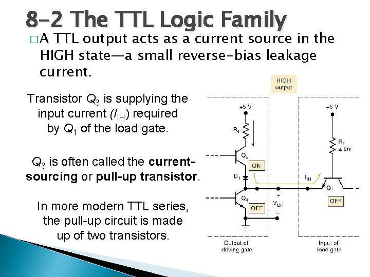
8 -2 The TTL Logic Family �A TTL output acts as a current source in the HIGH state—a small reverse-bias leakage current. Transistor Q 3 is supplying the input current (IIH) required by Q 1 of the load gate. Q 3 is often called the currentsourcing or pull-up transistor. In more modern TTL series, the pull-up circuit is made up of two transistors.

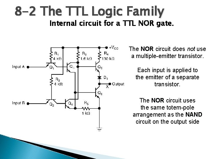
8 -2 The TTL Logic Family Internal circuit for a TTL NOR gate. The NOR circuit does not use a multiple-emitter transistor. Each input is applied to the emitter of a separate transistor. The NOR circuit uses the same totem-pole arrangement as the NAND circuit on the output side

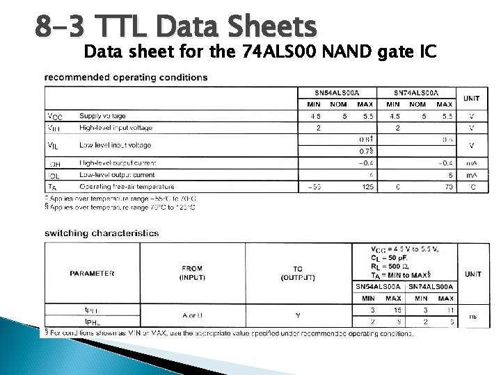
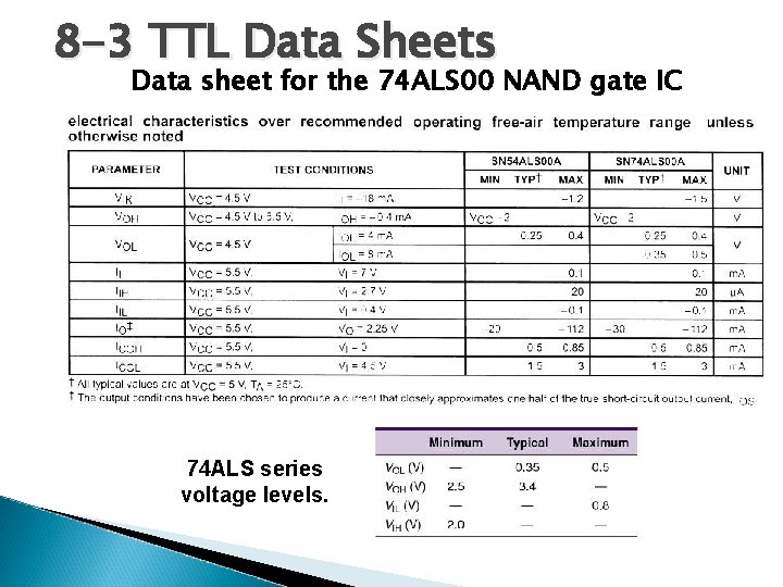
8 -3 TTL Data Sheets � The first line of TTL ICs was the 54/74 series from Texas Instruments—introduced in 1964. � Manufacturers use the same numbering system. ◦ Prefix indicates manufacturer. �SN – Texas Instruments. �DM – National Semiconductor. �S – Signetics. ◦ DM 7402, SN 7402, S 7402 perform the same function. � Data sheets contain electrical characteristics, switching characteristics, and recommended operating conditions.

8 -3 TTL Data Sheets Data sheet for the 74 ALS 00 NAND gate IC

8 -3 TTL Data Sheets Data sheet for the 74 ALS 00 NAND gate IC 74 ALS series voltage levels.

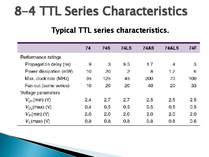
8 -4 TTL Series Characteristics Typical TTL series characteristics.

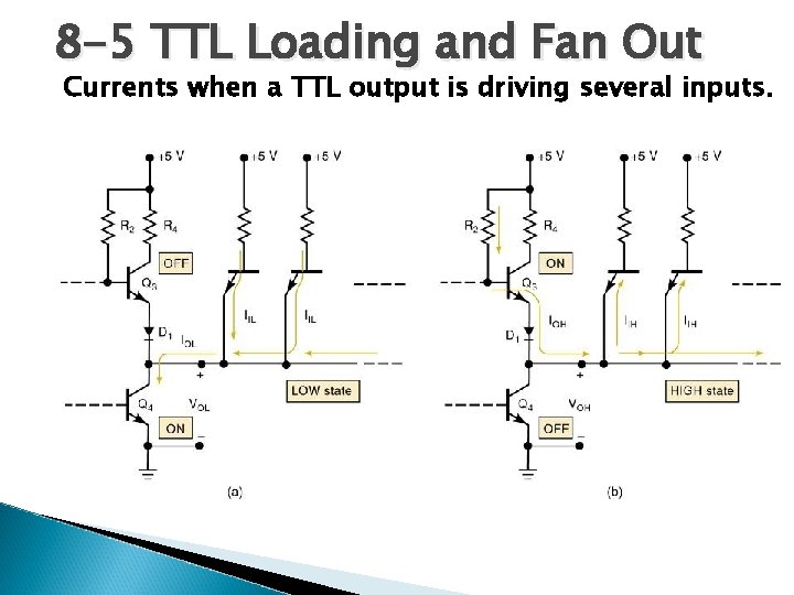
8 -5 TTL Loading and Fan-Out � Fan-out refers to the load drive capability of an IC output ◦ A TTL output has a limit on how much current it can sink in the LOW state, or source in the HIGH state. ◦ Exceeding these currents will result in output voltage levels outside specified ranges. � Determining fan out ◦ Add the IIH for all inputs connected to an output. �Sum must be less than the output IOH specification. ◦ Add the IIL for all inputs connected to an output. �Sum must be less than the output IOL specification.

8 -5 TTL Loading and Fan Out Currents when a TTL output is driving several inputs.

8 -6 Other TTL Characteristics � Unconnected (floating) inputs. ◦ On any TTL IC, all of the inputs are 1 s if they are not connected to some logic signal. �An input left unconnected, it is said to be floating.

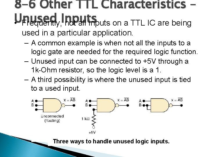
8 -6 Other TTL Characteristics – Unused • Frequently, Inputs not all inputs on a TTL IC are being used in a particular application. – A common example is when not all the inputs to a logic gate are needed for the required logic function. – Unused input can be connected to +5 V through a 1 k-Ohm resistor, so the logic level is a 1. – A third possibility is where the unused input is tied to a used input. Three ways to handle unused logic inputs.

8 -6 Other TTL Characteristics – Tied-Together Inputs � Two (or more) TTL inputs on the same gate connected to form a common input will generally represent a load that is the sum of the load current rating of each individual input. � The only exception is for NAND and AND gates. ◦ The LOW-state input load will be the same as a single input—no matter how many inputs are tied together.

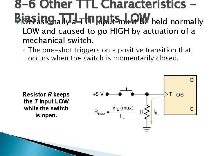
8 -6 Other TTL Characteristics – Biasing TTL Inputs LOW � Occasionally a TTL input must be held normally LOW and caused to go HIGH by actuation of a mechanical switch. ◦ The one-shot triggers on a positive transition that occurs when the switch is momentarily closed. Resistor R keeps the T input LOW while the switch is open.

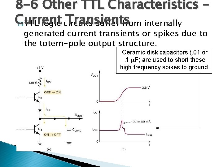
8 -6 Other TTL Characteristics – Current Transients � TTL logic circuits suffer from internally generated current transients or spikes due to the totem-pole output structure. Ceramic disk capacitors (. 01 or. 1 F) are used to short these high frequency spikes to ground.

8 -7 Technology � MOSMOS technology derives its name from the basic structure of a metal electrode, over an oxide insulator, over a semi-conductor substrate. ◦ Transistors of MOS technology are field-effect transistors—called MOSFETs. The electric field on the metal electrode side of the oxide insulator has an effect on the resistance of the substrate. • Most of the MOS digital ICs are constructed entirely of MOSFETs and no other components. – MOSFETs are relatively simple and inexpensive to fabricate, small, and consume very little power.

8 -7 Technology � The MOS principal disadvantage of MOS devices is their susceptibility to static-electricity damage. ◦ Although minimized by proper handling, TTL is still more durable for laboratory experimentation.

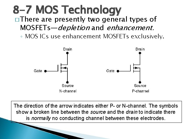
8 -7 MOS Technology � There are presently two general types of MOSFETs—depletion and enhancement. ◦ MOS ICs use enhancement MOSFETs exclusively. The direction of the arrow indicates either P- or N-channel. The symbols show a broken line between the source and the drain to indicate there is normally no conducting channel between these electrodes.

8 -7 MOS Technology – Basic MOSFET Switch � An N-channel MOSFET is the basic element in a family of devices known as N-MOS. ◦ Drain is always biased positive relative to the source.

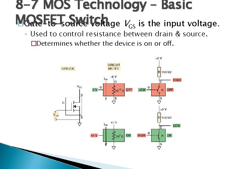
8 -7 MOS Technology – Basic MOSFET Switch � Gate-to-source voltage VGS is the input voltage. ◦ Used to control resistance between drain & source. �Determines whether the device is on or off.

8 -7 MOS Technology – Basic MOSFET Switch � The P-channel MOSFET—P-MOS—operates in the same manner as the N-channel. ◦ Except that it uses voltages of opposite polarity. � The drain is connected to the lower side of the circuit so it is biased with a more negative voltage relative to the source.

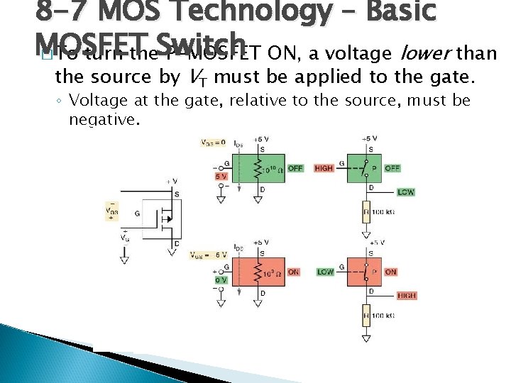
8 -7 MOS Technology – Basic MOSFET � To turn the. Switch P-MOSFET ON, a voltage lower than the source by VT must be applied to the gate. ◦ Voltage at the gate, relative to the source, must be negative.

8 -8 Complementary MOS Logic – CMOS Inverter � P-MOS & N-MOS circuits began to dominate the LSI and VLSI markets in the 1970 s and 1980 s. ◦ Use fewer components & are much simpler to manufacture than TTL circuits. � During this era, technology emerged that used P-MOS & N-MOS transistors in the same circuit. ◦ Complementary MOS, or CMOS, technology.

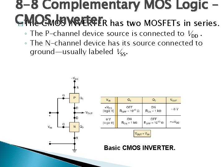
8 -8 Complementary MOS Logic – CMOS Inverter � The CMOS INVERTER has two MOSFETs in series. ◦ The P-channel device source is connected to VDD. ◦ The N-channel device has its source connected to ground—usually labeled VSS. Basic CMOS INVERTER.

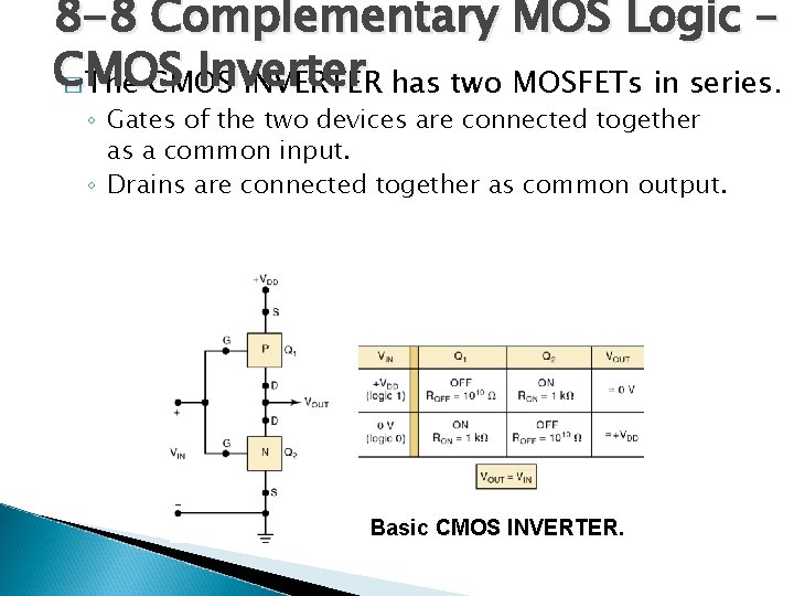
8 -8 Complementary MOS Logic – CMOS Inverter � The CMOS INVERTER has two MOSFETs in series. ◦ Gates of the two devices are connected together as a common input. ◦ Drains are connected together as common output. Basic CMOS INVERTER.

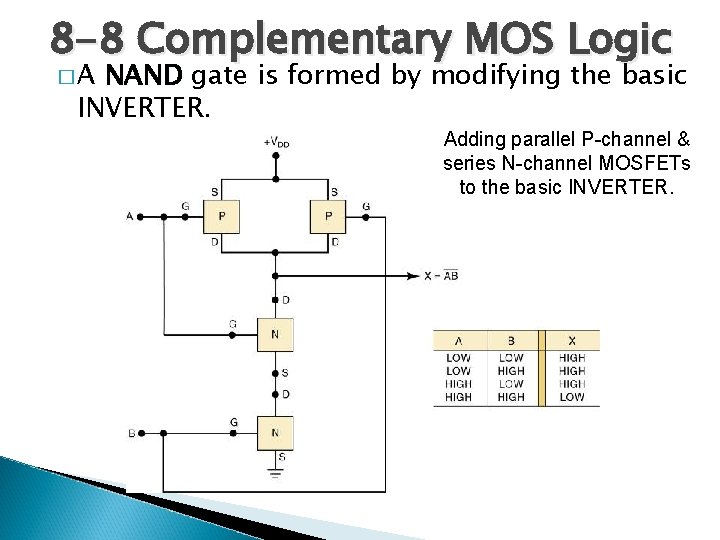
8 -8 Complementary MOS Logic �A NAND gate is formed by modifying the basic INVERTER. Adding parallel P-channel & series N-channel MOSFETs to the basic INVERTER.

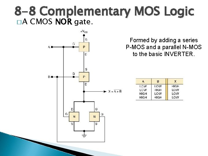
8 -8 Complementary MOS Logic �A CMOS NOR gate. Formed by adding a series P-MOS and a parallel N-MOS to the basic INVERTER.

8 -8 Complementary MOS Logic � Two CMOS NOR gates or NAND gates can be cross-coupled to form a simple SET-RESET latch ◦ Additional gating circuitry is used to convert the basic SET-RESET latch to clocked D and J-K flip-flops.

8 -9 CMOS Series Characteristics -� CMOS Terms ICs provide all TTL logic functions, and special-purpose functions not provided by TTL. � Terms used when ICs from different families or series are to be used together or as replacements. ◦ Pin-compatible—two ICs are pin-compatible when their pin configurations are the same. ◦ Functionally equivalent—ICs are functionally equivalent when the logic functions they perform are exactly the same. ◦ Electrically compatible—ICs are electrically compatible when they can be connected directly to each other without special measures to ensure properation.

8 -9 CMOS Series Characteristics –� The IC oldest Series CMOS series is the 4000 series by RCA—functionally equivalent to Motorola 14000. ◦ Rarely used in new designs except when a specialpurpose IC is not available in other series. � The 74 HC/HCT series has a 10 -fold increase in switching speed, comparable to 74 LS devices. ◦ Pin-compatible with, functionally equivalent to TTL ICs with the same device number. � The 74 AC/ACT series is often referred to as ACL for advanced CMOS logic. ◦ Functionally equivalent various TTL series, but not pin -compatible with TTL.

8 -9 CMOS Series Characteristics –� Series IC Series 74 AHC/AHCT offers a natural migration path from the HC series to faster, lower-power, low-drive applications. ◦ Three times faster, with similar noise immunity to HC without the over- under-shoot problems. � Bi. CMOS combines the best of bipolar & CMOS ◦ Characteristics are integrated to produce an extremely low-power, high-speed logic family. �Limited to functions used in microprocessor and bus interfacing applications.

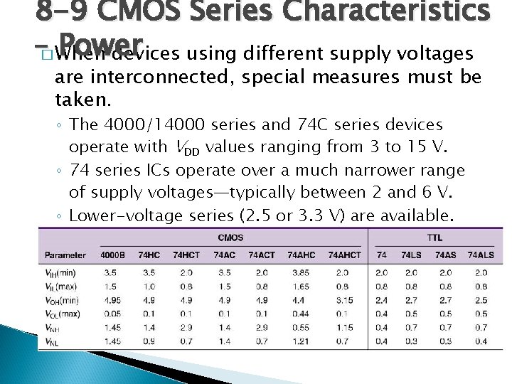
8 -9 CMOS Series Characteristics –� When Power devices using different supply voltages are interconnected, special measures must be taken. ◦ The 4000/14000 series and 74 C series devices operate with VDD values ranging from 3 to 15 V. ◦ 74 series ICs operate over a much narrower range of supply voltages—typically between 2 and 6 V. ◦ Lower-voltage series (2. 5 or 3. 3 V) are available.

8 -9 CMOS Series Characteristics –� In. Power general, CMOS devices have greater noise margins than TTL. � When a CMOS logic circuit is in a static state— not changing—its power dissipation is extremely low. ◦ Ideally suited for applications using battery power. � Power dissipation of a CMOS IC will be very low as long as it is in a dc condition. ◦ PD will increase in proportion to the frequency at which the circuits are switching states.

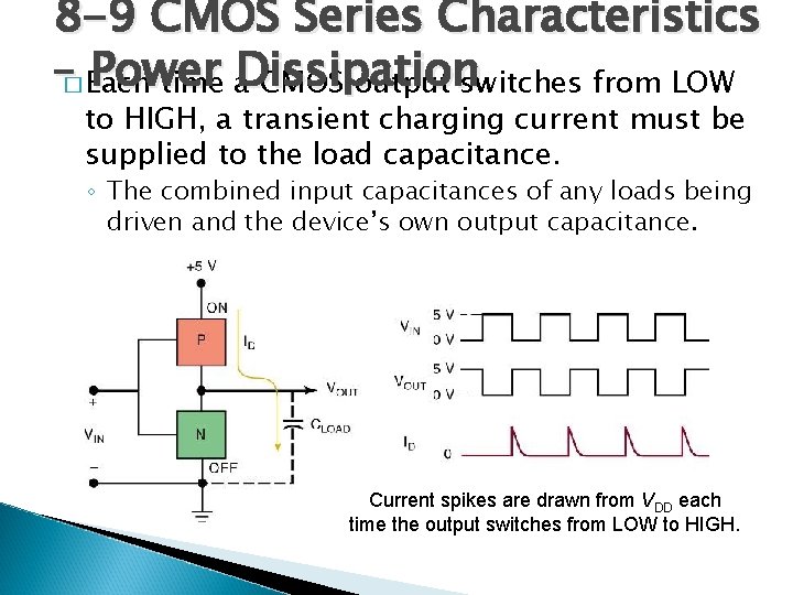
8 -9 CMOS Series Characteristics –� Each Power Dissipation time a CMOS output switches from LOW to HIGH, a transient charging current must be supplied to the load capacitance. ◦ The combined input capacitances of any loads being driven and the device’s own output capacitance. Current spikes are drawn from VDD each time the output switches from LOW to HIGH.

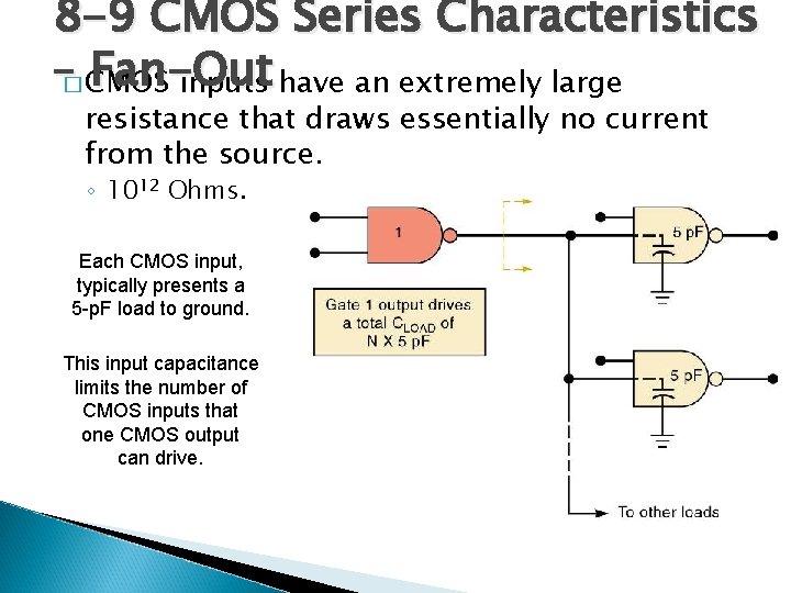
8 -9 CMOS Series Characteristics –� CMOS Fan-Out inputs have an extremely large resistance that draws essentially no current from the source. ◦ 1012 Ohms. Each CMOS input, typically presents a 5 -p. F load to ground. This input capacitance limits the number of CMOS inputs that one CMOS output can drive.

8 -9 CMOS Series Characteristics –� Although Switching CMOS Speed must drive relatively large load capacitances, switching speed is somewhat faster. ◦ Due to low output resistance in each state. � In the CMOS circuit, output resistance in the HIGH state is the RON of the P-MOSFET. ◦ Typically 1 -k Ohms or less.

8 -9 CMOS Series Characteristics –� All Static Sensitivity electronic devices, to varying degrees, are sensitive to damage by static electricity. ◦ MOS logic families are especially susceptible.

8 -9 CMOS Series Characteristics –� Precautions Static Sensitivity against Electrostatic discharge: ◦ Connect the chassis of all test instruments, solderingiron tips, and your metal workbench to earth ground. ◦ Connect yourself to ground with a special wrist strap. ◦ Keep ICs in conductive foam or aluminum foil. �So no dangerous voltages develop between any pins. ◦ Avoid touching IC pins—insert the IC into the circuit immediately after removing from the protective carrier. ◦ Place shorting straps across the edge connectors of PC boards when the boards are carried/transported. �Avoid touching the edge connectors. ◦ Do not leave any unused IC inputs unconnected. �Open inputs tend to pick up stray static charges.

8 -9 CMOS Series Characteristics –� Unavoidable Switching Speed existence of parasitic (unwanted) PNP and NPN transistors embedded in CMOS substrate can cause a condition called latch-up. ◦ If triggered, they will latch-up (stay ON permanently), and a large current will destroy the IC. � Most modern CMOS ICs are designed with protection circuitry that helps prevent latch-up ◦ It can still occur when the device’s maximum voltage ratings are exceeded. ◦ Latch-up can be triggered by high-voltage spikes or ringing at the device inputs and outputs.

8 -10 Low Voltage Technology � Increased chip density has major benefits: ◦ It allows more circuits to be packed onto the chip; �With the circuits closer together, the time for signals to propagate from one circuit to another will decrease. � There also drawbacks to higher chip density ◦ When circuits are closer together, insulating material that isolates one circuit from another is narrower. �Decreases the amount of voltage that the device can withstand before dielectric breakdown occurs. ◦ Chip power dissipation increases, which can raise chip temperature above maximum for reliable operation. �These drawbacks can be neutralized by operating the chip at lower volt-age levels,

8 -10 Low Voltage Technology – CMOS � Several low-voltage series are currently available: ◦ 74 LVC (Low-Voltage CMOS) series contains the widest assortment of the familiar SSI gates and MSI functions of the 5 -V families. ◦ 74 ALVC (Advanced Low-Voltage CMOS) offers the highest performance. ◦ 74 LV (Low-Voltage) series offers CMOS technology and many SSI gates/MSI logic functions, along with some popular octal buffers, latches, and flip-flops. ◦ 74 AVC (Advanced Very-Low-Voltage CMOS) series is optimized for 2. 5 -V systems. �It has many of the bus interface features of the Bi. CMOS series that will make it useful in future generations.

8 -10 Low Voltage Technology – CMOS � Several low-voltage series are currently available: ◦ 74 AUC (Advanced Ultra-Low-Voltage CMOS) series is optimized to operate at 1. 8 -V logic levels. ◦ 74 AUP (Advanced Ultra-low Power) is the lowestpower logic series—used in battery-operated portable applications. ◦ 74 CBT (Cross Bar Technology) series offers highspeed bus-interface circuits that can switch quickly. � 74 CBTLV (Cross Bar Technology Low Voltage) is the 3. 3 -V complement to the 74 CBT series. ◦ 74 GTLP (Gunning Transceiver Logic Plus) series is made for high-speed parallel backplane applications.

8 -10 Low Voltage Technology – CMOS � Several low-voltage series are currently available: ◦ 74 SSTV (Stub Series Terminated Logic) is useful in high -speed advanced-memory systems. ◦ TS Switch (TI Signal Switch) series is made for mixedsignal applications and offers some analog/digital switching & multiplexing solutions. ◦ 74 TVC (Translation Voltage Clamp) series is used to protect the inputs and outputs of sensitive devices from voltage overshoot on the bus lines.

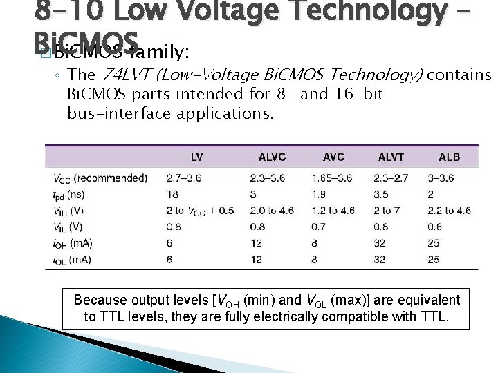
8 -10 Low Voltage Technology – Bi. CMOS � Bi. CMOS family: ◦ The 74 LVT (Low-Voltage Bi. CMOS Technology) contains Bi. CMOS parts intended for 8 - and 16 -bit bus-interface applications. Because output levels [VOH (min) and VOL (max)] are equivalent to TTL levels, they are fully electrically compatible with TTL.

8 -10 Low Voltage Technology � Bi. CMOS family: ◦ 74 ALVT (Advanced Low-Voltage Bi. CMOS Technology) series is an improvement over the LVT. �It offers 3. 3 -V or 2. 5 -V operation at 3 ns, pin-compatible with ABT and LVT, also intended for bus-interface uses. ◦ 74 ALB (Advanced Low-Voltage Bi. CMOS) series is designed for 3. 3 -V bus-interface applications. � 25 m. A output drive & propagation delays of only 2. 2 ns. ◦ 74 VME (VERSA Module Eurocard) series is designed to operate with the standard VME bus technology.

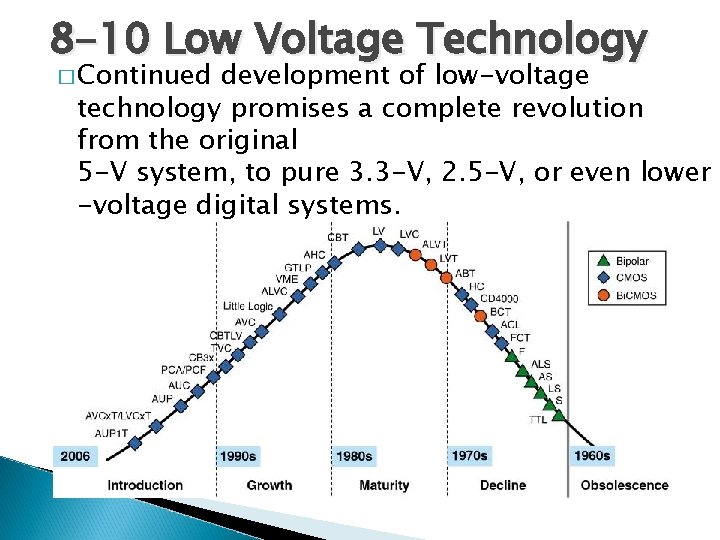
8 -10 Low Voltage Technology � Continued development of low-voltage technology promises a complete revolution from the original 5 -V system, to pure 3. 3 -V, 2. 5 -V, or even lower -voltage digital systems.

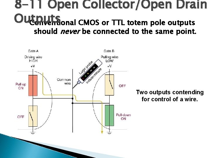
8 -11 Open Collector/Open Drain Outputs Conventional CMOS or TTL totem pole outputs should never be connected to the same point. Two outputs contending for control of a wire.

8 -11 Open Collector/Open Drain Outputs � One solution to the problem of sharing a common wire among gates is to remove the active pull-up transistor from each gate’s output circuit. ◦ In this way, none of the gates will ever try to assert a logic HIGH.

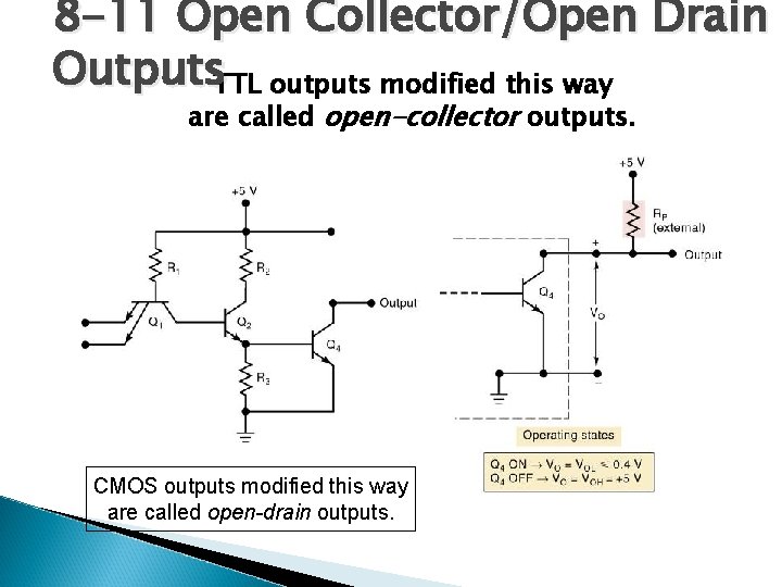
8 -11 Open Collector/Open Drain Outputs. TTL outputs modified this way are called open-collector outputs. CMOS outputs modified this way are called open-drain outputs.

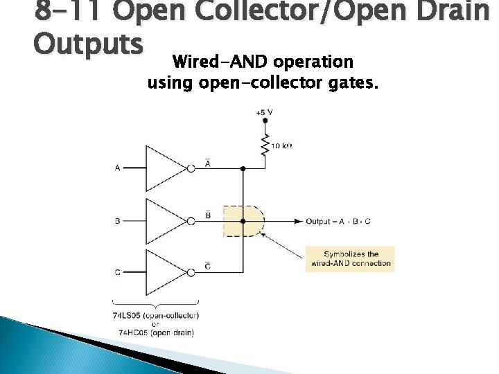
8 -11 Open Collector/Open Drain Outputs Wired-AND operation using open-collector gates.

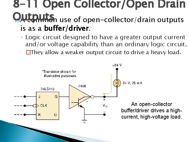
8 -11 Open Collector/Open Drain Outputs � A common use of open-collector/drain outputs is as a buffer/driver. ◦ Logic circuit designed to have a greater output current and/or voltage capability than an ordinary logic circuit. �They allow a weaker output circuit to drive a heavy load. An open-collector buffer/driver drives a highcurrent, high-voltage load.

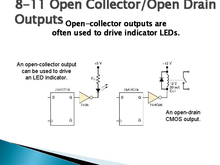
8 -11 Open Collector/Open Drain Outputs Open-collector outputs are often used to drive indicator LEDs. An open-collector output can be used to drive an LED indicator. An open-drain CMOS output.

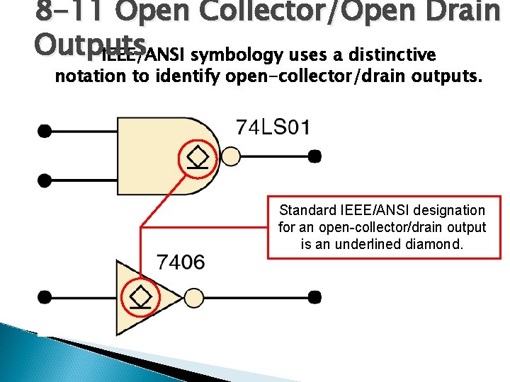
8 -11 Open Collector/Open Drain Outputs IEEE/ANSI symbology uses a distinctive notation to identify open-collector/drain outputs. Standard IEEE/ANSI designation for an open-collector/drain output is an underlined diamond.

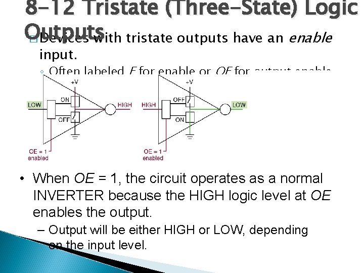
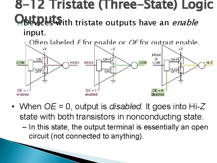
8 -12 Tristate (Three-State) Logic Outputs � The tristate configuration takes advantage of the high-speed operation of the pull-up/ pulldown output arrangement. ◦ While allowing outputs to be connected together to share a common wire. � Called tristate because it allows three possible output states: ◦ HIGH, LOW, and high-impedance (Hi-Z). � Hi-Z is a condition in which both pull-up & pull -down transistors are turned OFF. ◦ The output terminal is a high impedance to both ground and the power supply.

8 -12 Tristate (Three-State) Logic Outputs � Devices with tristate outputs have an enable input. ◦ Often labeled E for enable or OE for output enable. • When OE = 1, the circuit operates as a normal INVERTER because the HIGH logic level at OE enables the output. – Output will be either HIGH or LOW, depending on the input level.

8 -12 Tristate (Three-State) Logic Outputs � Devices with tristate outputs have an enable input. ◦ Often labeled E for enable or OE for output enable. • When OE = 0, output is disabled. It goes into Hi-Z state with both transistors in nonconducting state. – In this state, the output terminal is essentially an open circuit (not connected to anything).

8 -12 Tristate (Three-State) Logic Outputs � Outputs of tristate ICs can be connected together without sacrificing switching speed. ◦ When tristate outputs are connected together, only one of them should be enabled at one time. �Two active outputs could fight for control of the common wire. � Many ICs are designed with tristate outputs. ◦ 74 LS 374 is an octal D-type FF register IC with tristate outputs.

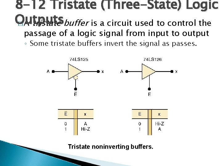
8 -12 Tristate (Three-State) Logic Outputs � A tristate buffer is a circuit used to control the passage of a logic signal from input to output ◦ Some tristate buffers invert the signal as passes. Tristate noninverting buffers.

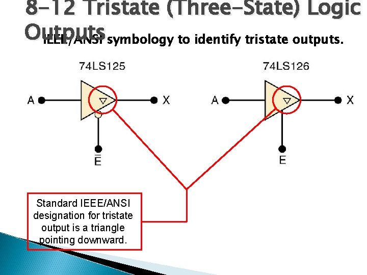
8 -12 Tristate (Three-State) Logic Outputs IEEE/ANSI symbology to identify tristate outputs. Standard IEEE/ANSI designation for tristate output is a triangle pointing downward.

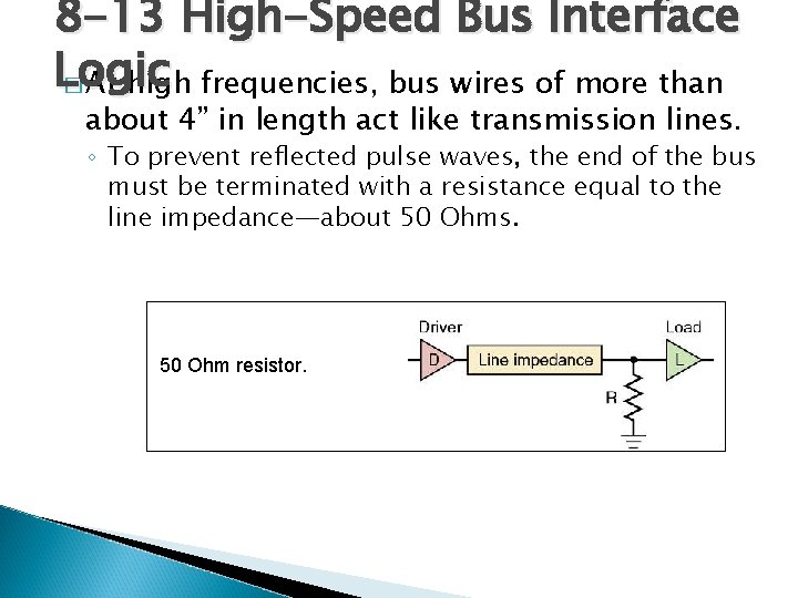
8 -13 High-Speed Bus Interface Logic � At high frequencies, bus wires of more than about 4” in length act like transmission lines. ◦ To prevent reflected pulse waves, the end of the bus must be terminated with a resistance equal to the line impedance—about 50 Ohms. 50 Ohm resistor.

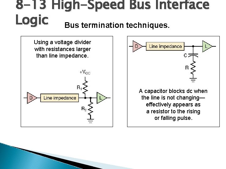
8 -13 High-Speed Bus Interface Logic Bus termination techniques. Using a voltage divider with resistances larger than line impedance. A capacitor blocks dc when the line is not changing— effectively appears as a resistor to the rising or falling pulse.

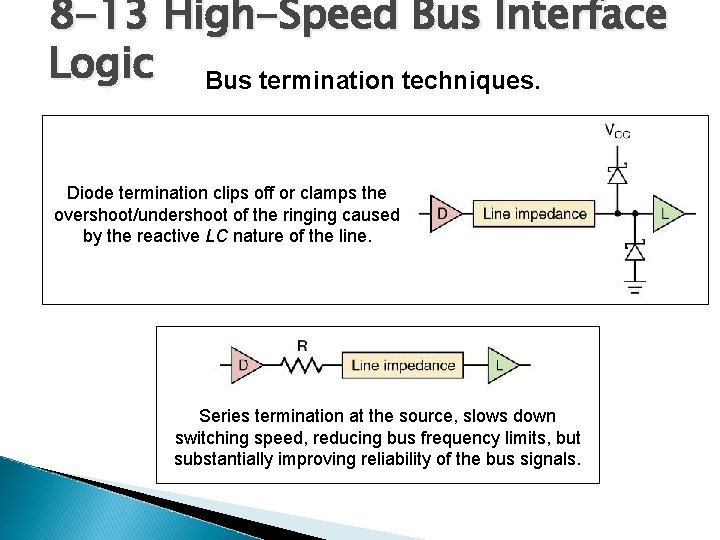
8 -13 High-Speed Bus Interface Logic Bus termination techniques. Diode termination clips off or clamps the overshoot/undershoot of the ringing caused by the reactive LC nature of the line. Series termination at the source, slows down switching speed, reducing bus frequency limits, but substantially improving reliability of the bus signals.

8 -13 High-Speed Bus Interface Logic � The GTLP (Gunning Transceiver Logic Plus) series of bus interface devices is specially designed to drive relatively long buses. � Low-voltage differential signaling (LVDS) uses two wires for each signal. ◦ Differential signaling means it responds to the difference between the two wires.

8 -14 The ECL Digital IC Family 8 -14 The ECL Digital ICfamily operates � The emitter-coupled logic (ECL) on the principle of current switching whereby… Family ◦ A fixed bias current less than I (sat) is switched C from one transistor’s collector to another. �Also referred to as current-mode logic (CML).

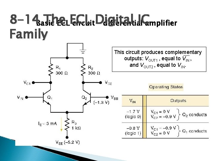
8 -14 The ECL Digital IC Family 8 -14 Basic The ICamplifier ECLECL circuit. Digital – differential Family This circuit produces complementary outputs: VOUT 1 , equal to VIN , and VOUT 2 , equal to VIN.

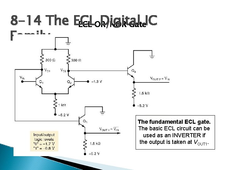
8 -14 The ECL Digital IC Family 8 -14 The ECL Digital ECL OR/ NOR Gate. IC OR Family The fundamental ECL gate. The basic ECL circuit can be used as an INVERTER if the output is taken at VOUT 1.

8 -14 The ECL Digital IC Family 8 -14 The ECL Digital IC � ECL characteristics: ◦ Very fast switching with typical propagation delay Family of 360 ps—faster than TTL or CMOS. ◦ The standard ECL logic levels are nominally -0. 8 V and 1. 7 V for logical 1 and 0 respectively. ◦ Worst-case noise margins approximately 150 m. V. ◦ ECL logic gates usually produce an output and its complement, eliminating the need for inverters. ◦ Current flow remains constant, eliminating noise spikes

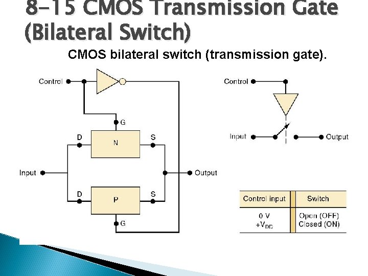
8 -15 CMOS Transmission Gate (Bilateral Switch) � A CMOS circuit with no TTL or ECL counterpart is the transmission gate or bilateral switch. ◦ Essentially acts as a single-pole, single-throw switch controlled by an input logic level. ◦ Passes signals in both directions—useful for digital and analog applications. ◦ Input must be between 0 and VDD volts.

8 -15 CMOS Transmission Gate (Bilateral Switch) CMOS bilateral switch (transmission gate).

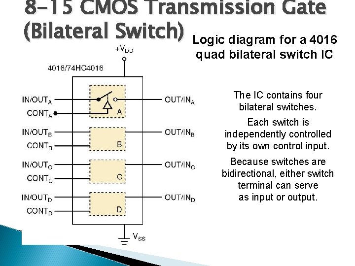
8 -15 CMOS Transmission Gate (Bilateral Switch) Logic diagram for a 4016 quad bilateral switch IC The IC contains four bilateral switches. Each switch is independently controlled by its own control input. Because switches are bidirectional, either switch terminal can serve as input or output.

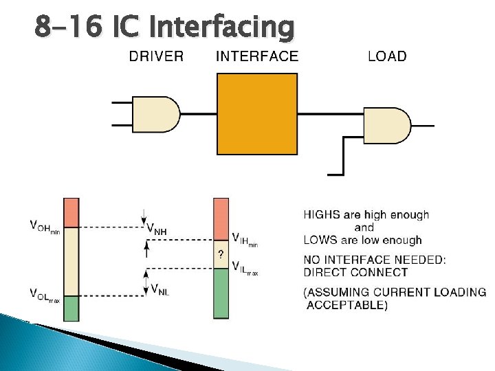
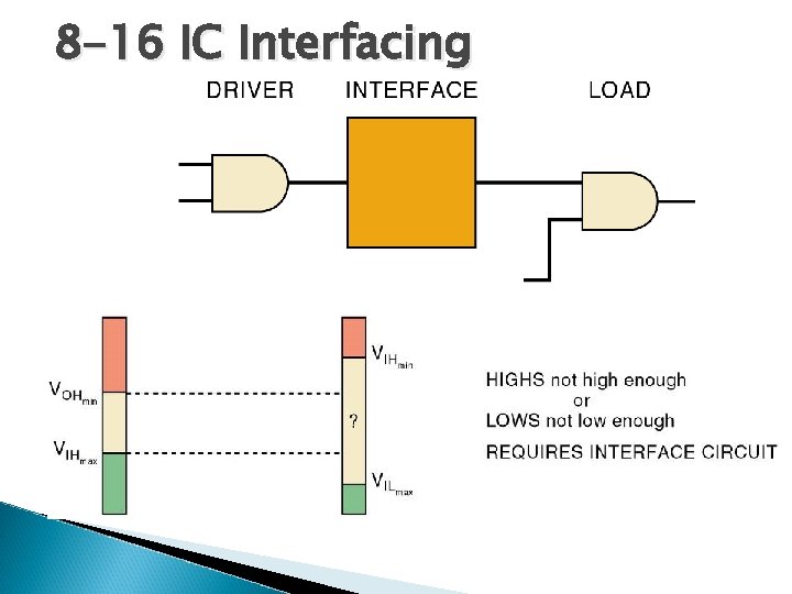
8 -16 IC Interfacing � Interfacing means connecting output(s) of one circuit/system to input(s) of another circuit/system. � The simplest and most desirable interface circuit between a driver and a load is a direct connection. ◦ Often a direct connection cannot be made due to a difference in electrical characteristics. � An interface circuit is connected between the driver and the load, to condition the driver output signal so it is compatible with requirements of the load.

8 -16 IC Interfacing

8 -16 IC Interfacing

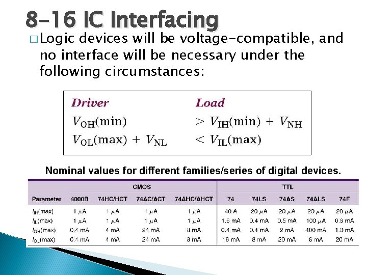
8 -16 IC Interfacing � Logic devices will be voltage-compatible, and no interface will be necessary under the following circumstances: Nominal values for different families/series of digital devices.

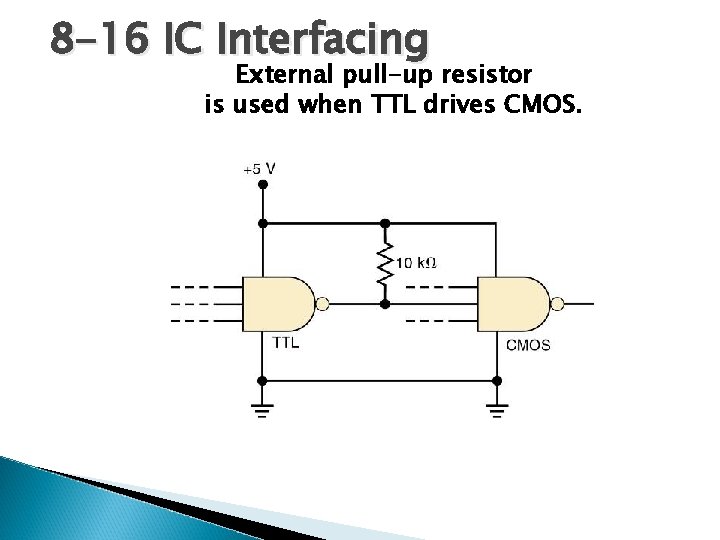
8 -16 IC Interfacing External pull-up resistor is used when TTL drives CMOS.

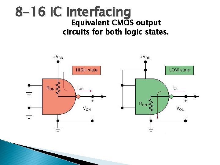
8 -16 IC Interfacing Equivalent CMOS output circuits for both logic states.

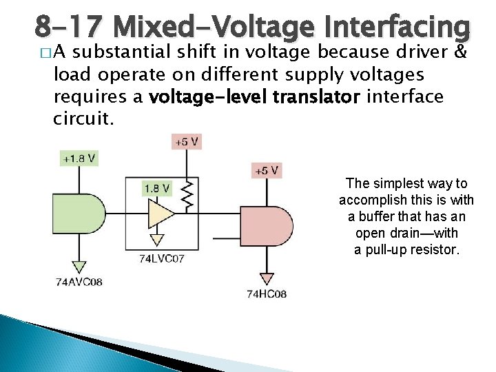
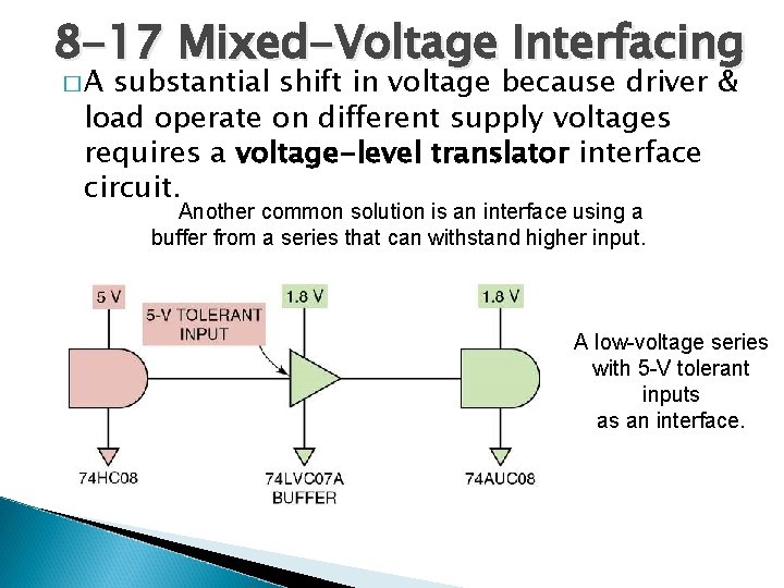
8 -17 Mixed-Voltage Interfacing �A substantial shift in voltage because driver & load operate on different supply voltages requires a voltage-level translator interface circuit. The simplest way to accomplish this is with a buffer that has an open drain—with a pull-up resistor.

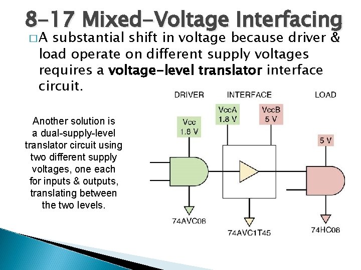
8 -17 Mixed-Voltage Interfacing �A substantial shift in voltage because driver & load operate on different supply voltages requires a voltage-level translator interface circuit. Another solution is a dual-supply-level translator circuit using two different supply voltages, one each for inputs & outputs, translating between the two levels.

8 -17 Mixed-Voltage Interfacing �A substantial shift in voltage because driver & load operate on different supply voltages requires a voltage-level translator interface circuit. Another common solution is an interface using a buffer from a series that can withstand higher input. A low-voltage series with 5 -V tolerant inputs as an interface.

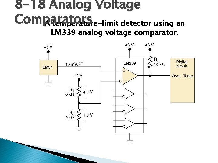
8 -18 Analog Voltage Comparators � Another very useful device for interfacing to digital systems is the analog voltage comparator. ◦ An comparator compares two voltages. �If (+) input voltage is greater than (-) input voltage, the output is HIGH. �If (-) input voltage is greater than (+) input voltage, the output is LOW. � Comparator inputs can be thought of as analog. ◦ Output is digital—always either HIGH or LOW. � The comparator is often referred to as a one-bit analog-to-digital (A/D) converter.

8 -18 Analog Voltage Comparators A temperature-limit detector using an LM 339 analog voltage comparator.

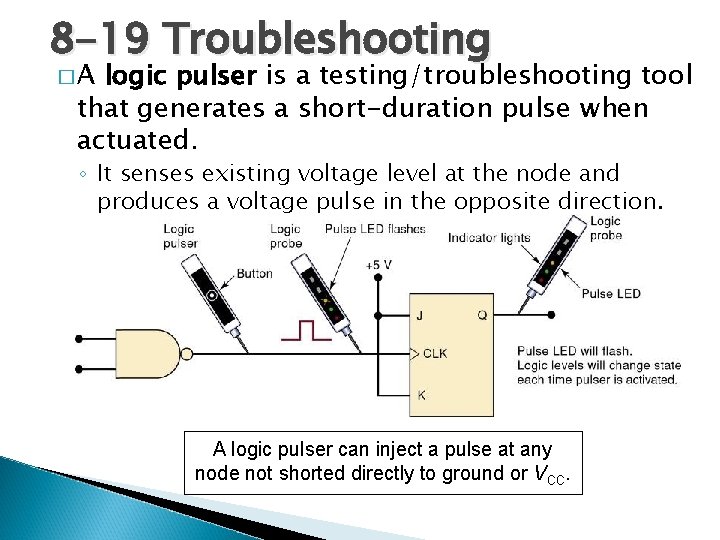
8 -19 Troubleshooting �A logic pulser is a testing/troubleshooting tool that generates a short-duration pulse when actuated. ◦ It senses existing voltage level at the node and produces a voltage pulse in the opposite direction. A logic pulser can inject a pulse at any node not shorted directly to ground or VCC.

8 -20 Characteristics of an FPGA � Consider the electrical and timing characteristics for the Altera Cyclone™ II family of devices. ◦ A subcategory of PLD devices referred to as field programmable gate arrays (FPGAs). � Two different power-supply voltages must be applied to a Cyclone II chip. ◦ VCCINT provides power for the internal logic of the chip. �The nominal value is 1. 2 V ◦ A separate supply voltage, VCCIO , will power the input and output buffers of the Cyclone chips.

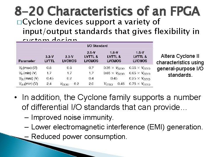
8 -20 Characteristics of an FPGA � Cyclone devices support a variety of input/output standards that gives flexibility in system design. Altera Cyclone II characteristics using general-purpose I/O standards. • In addition, the Cyclone family supports a number of differential I/O standards that can provide… – Improved noise immunity. – Lower electromagnetic interference (EMI) generation. – Reduced power consumption.

8 -20 Characteristics of an FPGA � The Cyclone II devices use CMOS, so power consumption will be low—power will be dependent on voltage level, frequencies & I/O signal loads. � The Quartus II software has two tools to estimate the amount the power usage for an application ◦ The Power. Play Early Power Estimator is typically used during the early stages of design ◦ The Power. Play Power Analyzer is often used with sample test vectors, for more accurate estimate.

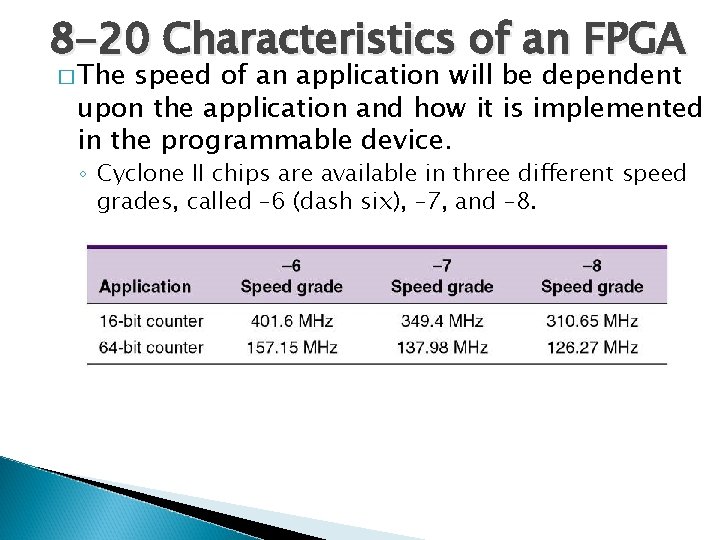
8 -20 Characteristics of an FPGA � The speed of an application will be dependent upon the application and how it is implemented in the programmable device. ◦ Cyclone II chips are available in three different speed grades, called – 6 (dash six), – 7, and – 8.

END