Rayat Shikshan Sansthas S M Joshi College Hadapsar028

- Slides: 33
Rayat Shikshan Sanstha’s S. M. Joshi College Hadapsar-028 Department of Electronics Science Passive Components Presented by. Dr. Kakade P. K
Op-Amp � Introduction of Operation Amplifier (Op-Amp) � Block Diagram � Analysis of ideal Op-Amp applications � Comparison of ideal and non-ideal Op-Amp � Non-ideal Op-Amp consideration Operational Amplifier 2
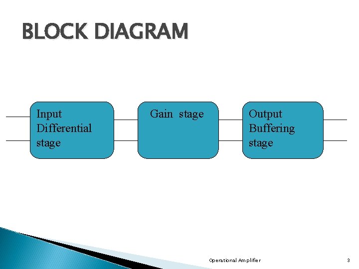
BLOCK DIAGRAM Input Differential stage Gain stage Output Buffering stage Operational Amplifier 3
Stages � Input Differential Stage � Intermediate � Output � Current Signal-Ended High-Gain Stage Buffering Stage Source / Short Circuit Protection
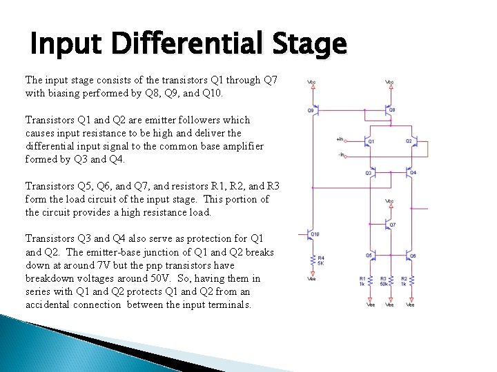
Input Differential Stage The input stage consists of the transistors Q 1 through Q 7 with biasing performed by Q 8, Q 9, and Q 10. Transistors Q 1 and Q 2 are emitter followers which causes input resistance to be high and deliver the differential input signal to the common base amplifier formed by Q 3 and Q 4. Transistors Q 5, Q 6, and Q 7, and resistors R 1, R 2, and R 3 form the load circuit of the input stage. This portion of the circuit provides a high resistance load. Transistors Q 3 and Q 4 also serve as protection for Q 1 and Q 2. The emitter-base junction of Q 1 and Q 2 breaks down at around 7 V but the pnp transistors have breakdown voltages around 50 V. So, having them in series with Q 1 and Q 2 protects Q 1 and Q 2 from an accidental connection between the input terminals.
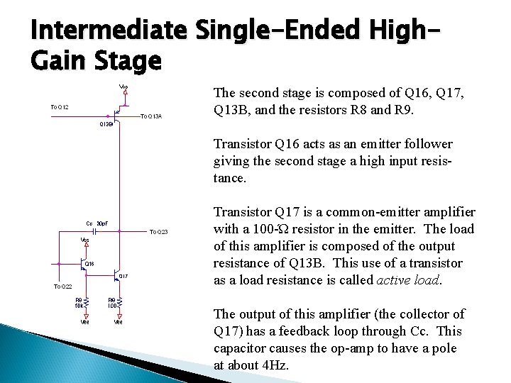
Intermediate Single-Ended High. Gain Stage The second stage is composed of Q 16, Q 17, Q 13 B, and the resistors R 8 and R 9. Transistor Q 16 acts as an emitter follower giving the second stage a high input resistance. Transistor Q 17 is a common-emitter amplifier with a 100 -Ώ resistor in the emitter. The load of this amplifier is composed of the output resistance of Q 13 B. This use of a transistor as a load resistance is called active load. The output of this amplifier (the collector of Q 17) has a feedback loop through Cc. This capacitor causes the op-amp to have a pole at about 4 Hz.
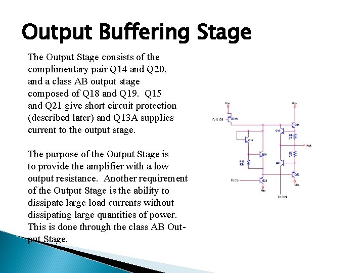
Output Buffering Stage The Output Stage consists of the complimentary pair Q 14 and Q 20, and a class AB output stage composed of Q 18 and Q 19. Q 15 and Q 21 give short circuit protection (described later) and Q 13 A supplies current to the output stage. The purpose of the Output Stage is to provide the amplifier with a low output resistance. Another requirement of the Output Stage is the ability to dissipate large load currents without dissipating large quantities of power. This is done through the class AB Output Stage.
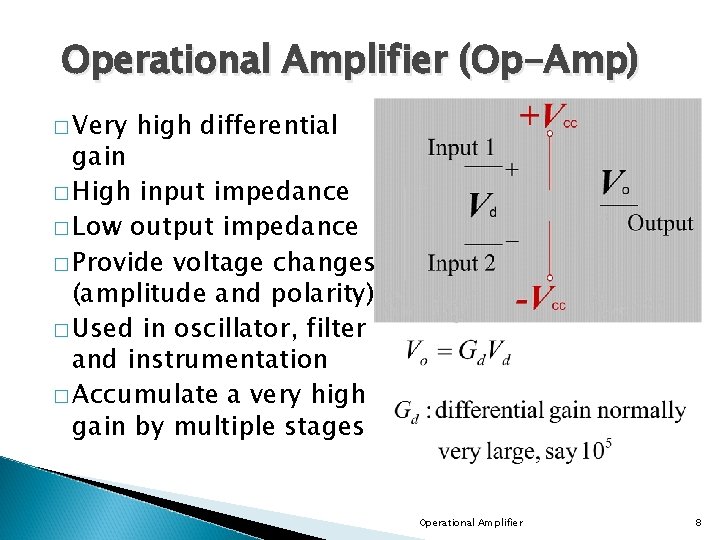
Operational Amplifier (Op-Amp) � Very high differential gain � High input impedance � Low output impedance � Provide voltage changes (amplitude and polarity) � Used in oscillator, filter and instrumentation � Accumulate a very high gain by multiple stages Operational Amplifier 8
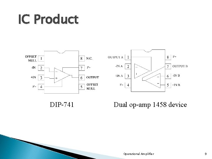
IC Product DIP-741 Dual op-amp 1458 device Operational Amplifier 9
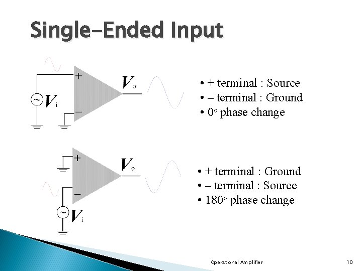
Single-Ended Input • + terminal : Source • – terminal : Ground • 0 o phase change • + terminal : Ground • – terminal : Source • 180 o phase change Operational Amplifier 10
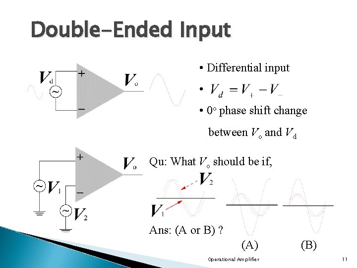
Double-Ended Input • Differential input • • 0 o phase shift change between Vo and Vd Qu: What Vo should be if, Ans: (A or B) ? (A) Operational Amplifier (B) 11
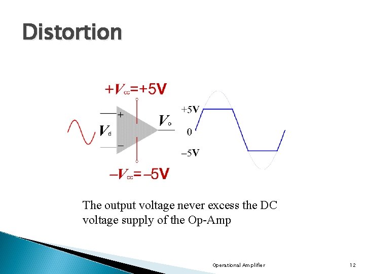
Distortion The output voltage never excess the DC voltage supply of the Op-Amp Operational Amplifier 12
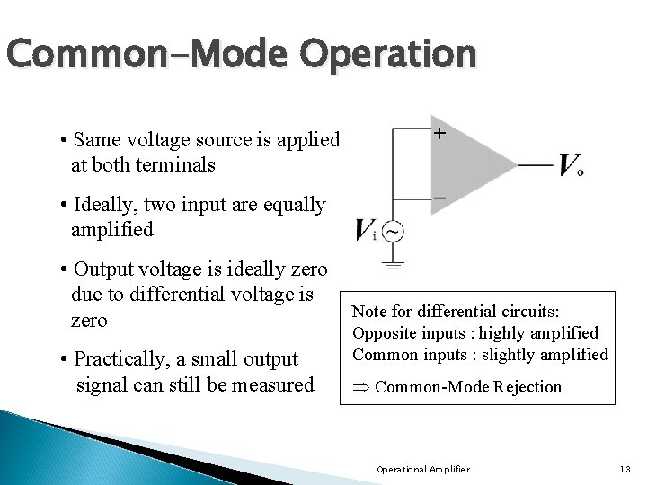
Common-Mode Operation • Same voltage source is applied at both terminals • Ideally, two input are equally amplified • Output voltage is ideally zero due to differential voltage is zero • Practically, a small output signal can still be measured Note for differential circuits: Opposite inputs : highly amplified Common inputs : slightly amplified Common-Mode Rejection Operational Amplifier 13
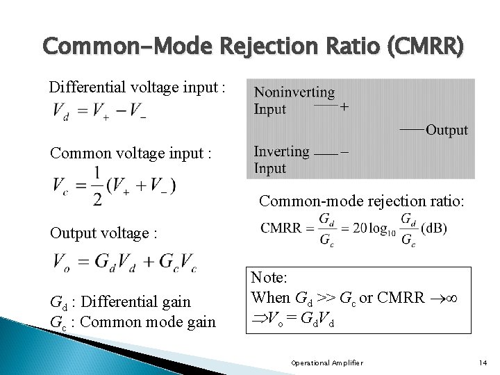
Common-Mode Rejection Ratio (CMRR) Differential voltage input : Common voltage input : Common-mode rejection ratio: Output voltage : Gd : Differential gain Gc : Common mode gain Note: When Gd >> Gc or CMRR Vo = Gd. Vd Operational Amplifier 14
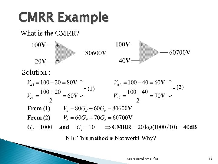
CMRR Example What is the CMRR? Solution : (2) (1) NB: This method is Not work! Why? Operational Amplifier 15
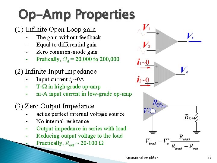
Op-Amp Properties (1) Infinite Open Loop gain - The gain without feedback Equal to differential gain Zero common-mode gain Pratically, Gd = 20, 000 to 200, 000 (2) Infinite Input impedance - Input current ii ~0 A T- in high-grade op-amp m-A input current in low-grade op-amp (3) Zero Output Impedance - act as perfect internal voltage source No internal resistance Output impedance in series with load Reducing output voltage to the load Practically, Rout ~ 20 -100 Operational Amplifier 16
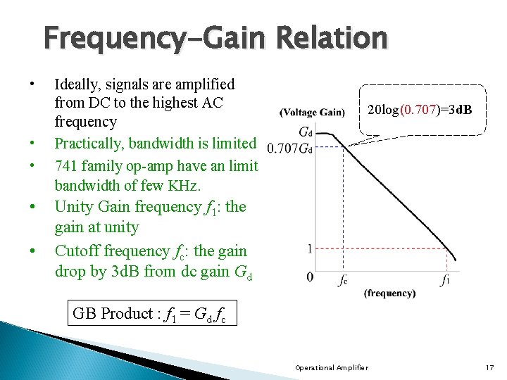
Frequency-Gain Relation • • • Ideally, signals are amplified from DC to the highest AC frequency Practically, bandwidth is limited 741 family op-amp have an limit bandwidth of few KHz. 20 log(0. 707)=3 d. B Unity Gain frequency f 1: the gain at unity Cutoff frequency fc: the gain drop by 3 d. B from dc gain Gd GB Product : f 1 = Gd fc Operational Amplifier 17
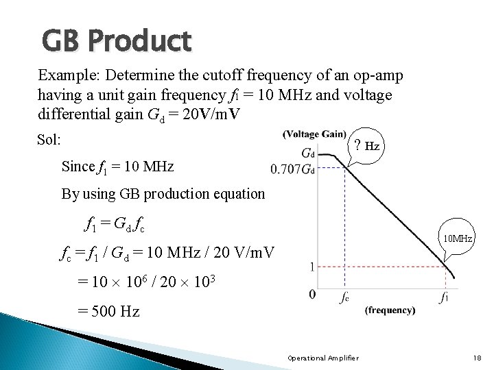
GB Product Example: Determine the cutoff frequency of an op-amp having a unit gain frequency f 1 = 10 MHz and voltage differential gain Gd = 20 V/m. V Sol: ? Hz Since f 1 = 10 MHz By using GB production equation f 1 = Gd f c 10 MHz fc = f 1 / Gd = 10 MHz / 20 V/m. V = 10 106 / 20 103 = 500 Hz Operational Amplifier 18
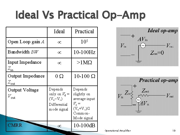
Ideal Vs Practical Op-Amp Ideal Practical Open Loop gain A 105 Bandwidth BW 10 -100 Hz Input Impedance Zin >1 M 0 10 -100 Depends only on Vd = (V+ V ) Differential mode signal Depends slightly on average input Vc = (V++V )/2 Common. Mode signal 10 -100 d. B Output Impedance Zout Output Voltage Vout CMRR Operational Amplifier 19
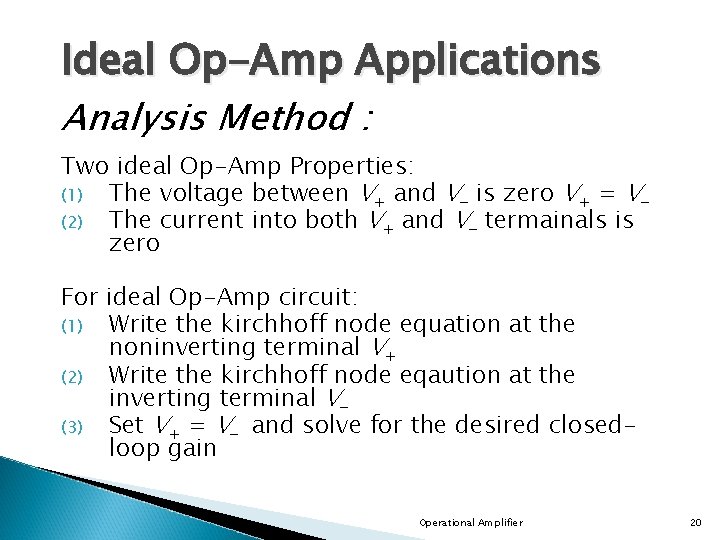
Ideal Op-Amp Applications Analysis Method : Two ideal Op-Amp Properties: (1) The voltage between V+ and V is zero V+ = V (2) The current into both V+ and V termainals is zero For ideal Op-Amp circuit: (1) Write the kirchhoff node equation at the noninverting terminal V+ (2) Write the kirchhoff node eqaution at the inverting terminal V (3) Set V+ = V and solve for the desired closedloop gain Operational Amplifier 20
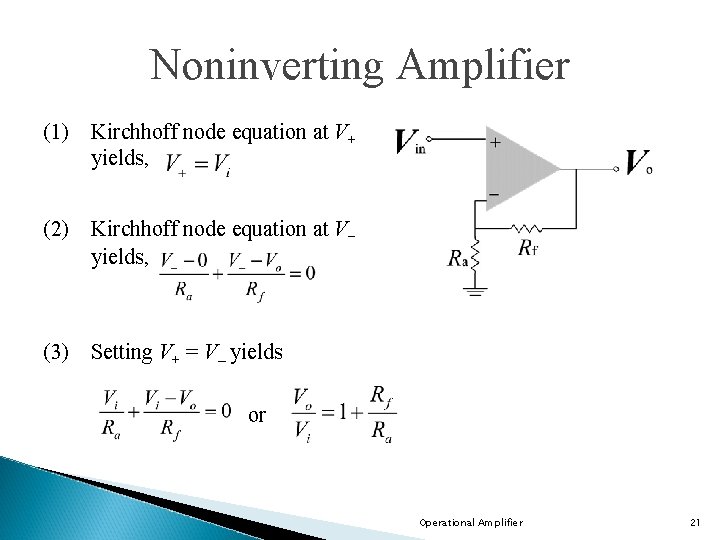
Noninverting Amplifier (1) Kirchhoff node equation at V+ yields, (2) Kirchhoff node equation at V yields, (3) Setting V+ = V– yields or Operational Amplifier 21
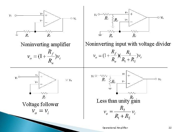
Noninverting amplifier Voltage follower Noninverting input with voltage divider Less than unity gain Operational Amplifier 22
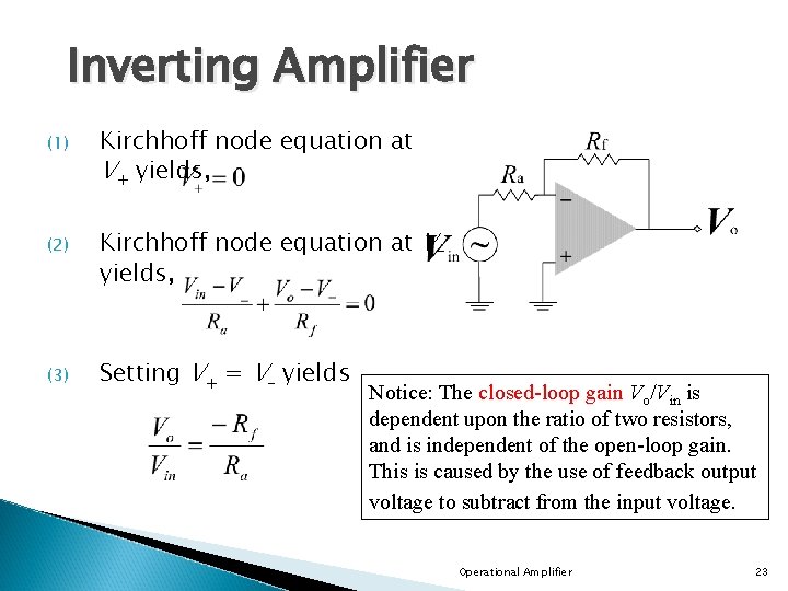
Inverting Amplifier (1) (2) (3) Kirchhoff node equation at V+ yields, Kirchhoff node equation at V yields, Setting V+ = V– yields Notice: The closed-loop gain Vo/Vin is dependent upon the ratio of two resistors, and is independent of the open-loop gain. This is caused by the use of feedback output voltage to subtract from the input voltage. Operational Amplifier 23
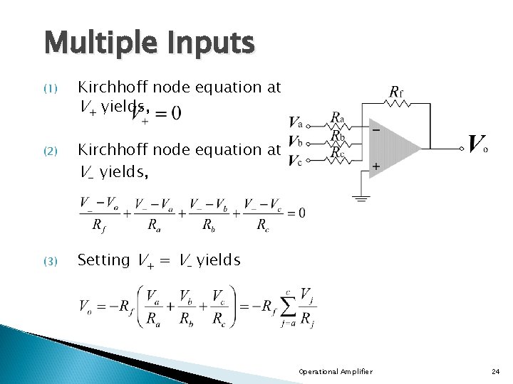
Multiple Inputs (1) Kirchhoff node equation at V+ yields, (2) Kirchhoff node equation at V yields, (3) Setting V+ = V– yields Operational Amplifier 24
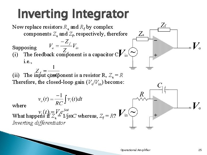
Inverting Integrator Now replace resistors Ra and Rf by complex components Za and Zf, respectively, therefore Supposing (i) The feedback component is a capacitor C, i. e. , (ii) The input component is a resistor R, Za = R Therefore, the closed-loop gain (Vo/Vin) become: where What happens if Za = 1/j C whereas, Zf = R? Inverting differentiator Operational Amplifier 25
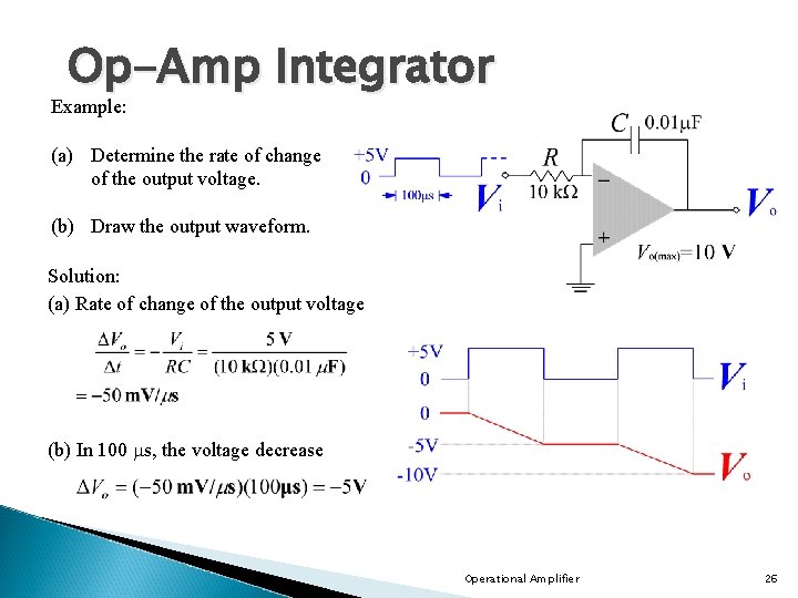
Op-Amp Integrator Example: (a) Determine the rate of change of the output voltage. (b) Draw the output waveform. Solution: (a) Rate of change of the output voltage (b) In 100 s, the voltage decrease Operational Amplifier 26
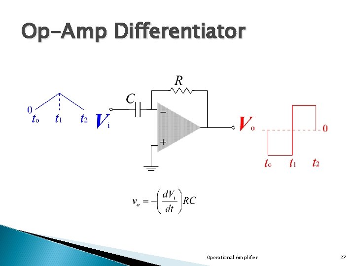
Op-Amp Differentiator Operational Amplifier 27
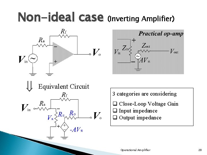
Non-ideal case (Inverting Amplifier) Equivalent Circuit 3 categories are considering q Close-Loop Voltage Gain q Input impedance q Output impedance Operational Amplifier 28
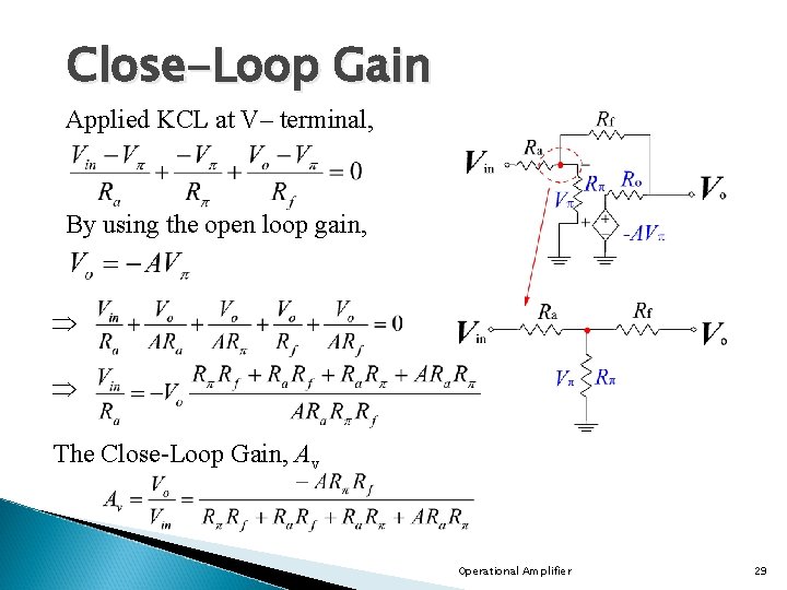
Close-Loop Gain Applied KCL at V– terminal, By using the open loop gain, The Close-Loop Gain, Av Operational Amplifier 29
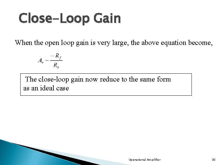
Close-Loop Gain When the open loop gain is very large, the above equation become, The close-loop gain now reduce to the same form as an ideal case Operational Amplifier 30
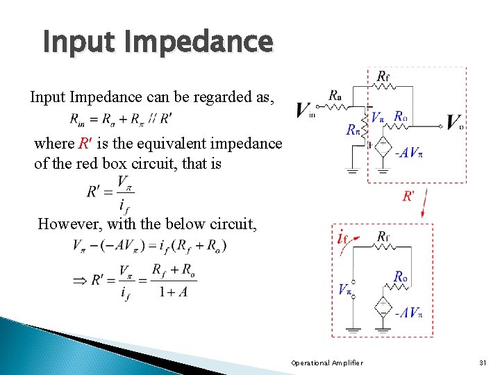
Input Impedance can be regarded as, where R is the equivalent impedance of the red box circuit, that is However, with the below circuit, Operational Amplifier 31
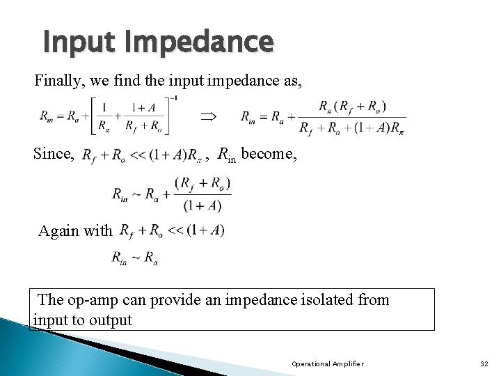
Input Impedance Finally, we find the input impedance as, Since, , Rin become, Again with The op-amp can provide an impedance isolated from input to output Operational Amplifier 32
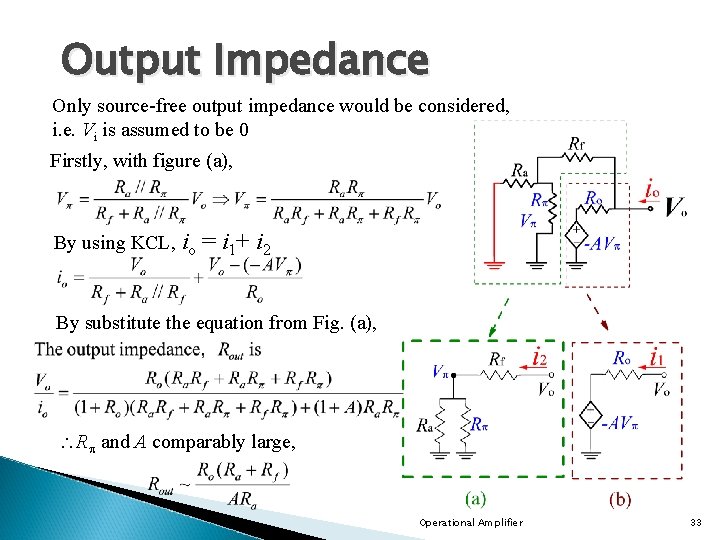
Output Impedance Only source-free output impedance would be considered, i. e. Vi is assumed to be 0 Firstly, with figure (a), By using KCL, io = i 1+ i 2 By substitute the equation from Fig. (a), R and A comparably large, Operational Amplifier 33