OnChip Communication Architectures Models for Power and Thermal
![Bus Wire Power Models Chern et al. [EDL ‘ 92] proposed a model for Bus Wire Power Models Chern et al. [EDL ‘ 92] proposed a model for](https://slidetodoc.com/presentation_image_h2/165812980931d609cb385b23bab13772/image-10.jpg)
![Bus Wire Power Models More accurate analytical models (Ho et al. [IEEE 2001]) combine Bus Wire Power Models More accurate analytical models (Ho et al. [IEEE 2001]) combine](https://slidetodoc.com/presentation_image_h2/165812980931d609cb385b23bab13772/image-12.jpg)
![Coupling-Aware Wire Power Models Kretzschmar et al. [DATE ‘ 04] proposed an analytical model Coupling-Aware Wire Power Models Kretzschmar et al. [DATE ‘ 04] proposed an analytical model](https://slidetodoc.com/presentation_image_h2/165812980931d609cb385b23bab13772/image-17.jpg)
![Coupling-Aware Wire Power Models Gupta et al. [ICCAD 2003] proposed a bus power model Coupling-Aware Wire Power Models Gupta et al. [ICCAD 2003] proposed a bus power model](https://slidetodoc.com/presentation_image_h2/165812980931d609cb385b23bab13772/image-19.jpg)
![Power Estimation of On-Chip Communication Architectures Lahiri et al. [CODES+ISSS 2004] proposed gate level Power Estimation of On-Chip Communication Architectures Lahiri et al. [CODES+ISSS 2004] proposed gate level](https://slidetodoc.com/presentation_image_h2/165812980931d609cb385b23bab13772/image-24.jpg)
![Power Estimation of On-Chip Communication Architectures Pasricha et al. [CODES+ISSS 2006] proposed an energy Power Estimation of On-Chip Communication Architectures Pasricha et al. [CODES+ISSS 2006] proposed an energy](https://slidetodoc.com/presentation_image_h2/165812980931d609cb385b23bab13772/image-26.jpg)
![Power Estimation of On-Chip Communication Architectures Caldari et al. [DATE 2003] proposed energy macro Power Estimation of On-Chip Communication Architectures Caldari et al. [DATE 2003] proposed energy macro](https://slidetodoc.com/presentation_image_h2/165812980931d609cb385b23bab13772/image-35.jpg)
![Power Estimation of On-Chip Communication Architectures Bona et al. [DATE 2004] proposed macro-models to Power Estimation of On-Chip Communication Architectures Bona et al. [DATE 2004] proposed macro-models to](https://slidetodoc.com/presentation_image_h2/165812980931d609cb385b23bab13772/image-37.jpg)
![Models for Thermal Estimation Sotiriadis et al. [TVLSI 2002] proposed a model for the Models for Thermal Estimation Sotiriadis et al. [TVLSI 2002] proposed a model for the](https://slidetodoc.com/presentation_image_h2/165812980931d609cb385b23bab13772/image-43.jpg)
![Models for Thermal Estimation Sundaresan et al. [VLSID 2005] proposed anothermal model for bus Models for Thermal Estimation Sundaresan et al. [VLSID 2005] proposed anothermal model for bus](https://slidetodoc.com/presentation_image_h2/165812980931d609cb385b23bab13772/image-45.jpg)
![PVT Variation-aware Power Estimation Pasricha et al. [VLSID 2008] presented several experimental results to PVT Variation-aware Power Estimation Pasricha et al. [VLSID 2008] presented several experimental results to](https://slidetodoc.com/presentation_image_h2/165812980931d609cb385b23bab13772/image-50.jpg)



- Slides: 57

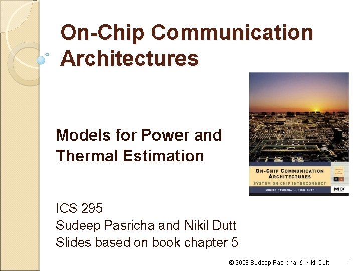
On-Chip Communication Architectures Models for Power and Thermal Estimation ICS 295 Sudeep Pasricha and Nikil Dutt Slides based on book chapter 5 © 2008 Sudeep Pasricha & Nikil Dutt 1

Outline Introduction Models for Power Estimation of Wires Models for Power Estimation of On-Chip Communication Architectures Models PVT for Thermal Estimation variation-aware Power Estimation © 2008 Sudeep Pasricha & Nikil Dutt 2

Introduction Power today is an important multi-processor systemon-chip (MPSo. C) design constraint ◦ for mobile applications such as cellular phones, MP 3 players, and laptops with fixed battery budgets e. g. , watching several movies on a single battery charge is virtually impossible on today’s devices ◦ for non-portable applications server farms e. g. , as much as 2 megawatts for a 25, 000 square foot server farm with 8000 servers In future silicon technologies increasing operating frequencies and transistor densities will make power dissipation a major concern Note: Power, Energy used interchangeably from here onwards © 2008 Sudeep Pasricha & Nikil Dutt 3

Introduction Power dissipation has an undesirable thermal side effect of increasing device temperature -> affects reliability of MPSo. Cs ◦ Reliability: probability that system will operate correctly at any given time of operation measured by mean time to failure (MTTF) Need to extend MTTF beyond expected life of a product ◦ for critical systems used in aircraft control, automotive control, medical equipment, defense applications Temperature cycles/spikes due to excessive power dissipation cause: ◦ Specific failure in components/wires ◦ Secondary effects such as timing failure and data corruption Techniques to estimate and reduce power consumption are essential for lowering operating temperatures © 2008 Sudeep Pasricha & Nikil Dutt 4

Introduction On-chip communication architectures have a considerable impact on MPSo. C power dissipation in DSM technologies ◦ coupling/parasitic capacitance increasingly dominant ◦ interconnect capacitance a large portion of chip capacitance ◦ large number of repeaters and vias to reduce wire delay in DSM technologies doubles power dissipation in interconnects ◦ state of the art communication architectures also have significant amounts of hardware logic e. g. , bridges, arbiters, decoders, buffers, etc. comparable to logic in embedded processors of moderate complexity © 2008 Sudeep Pasricha & Nikil Dutt 5

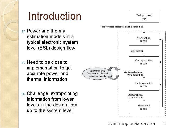
Introduction Power and thermal estimation models in a typical electronic system level (ESL) design flow Need to be close to implementation to get accurate power and thermal information Challenge: extrapolating information from lower levels in the design flow up to the system level © 2008 Sudeep Pasricha & Nikil Dutt 6

Outline Introduction Models for Power Estimation of Wires Models for Power Estimation of On-Chip Communication Architectures Models PVT for Thermal Estimation variation-aware Power Estimation © 2008 Sudeep Pasricha & Nikil Dutt 7

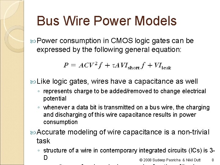
Bus Wire Power Models Power consumption in CMOS logic gates can be expressed by the following general equation: Like logic gates, wires have a capacitance as well ◦ represents charge to be added/removed to change electrical potential ◦ whenever a data bit is transmitted on a bus wire, the charging and discharging of this wire capacitance results in power consumption Accurate modeling of wire capacitance is a non-trivial task ◦ structure of a wire in contemporary integrated circuits (ICs) is 3 D © 2008 Sudeep Pasricha & Nikil Dutt 8

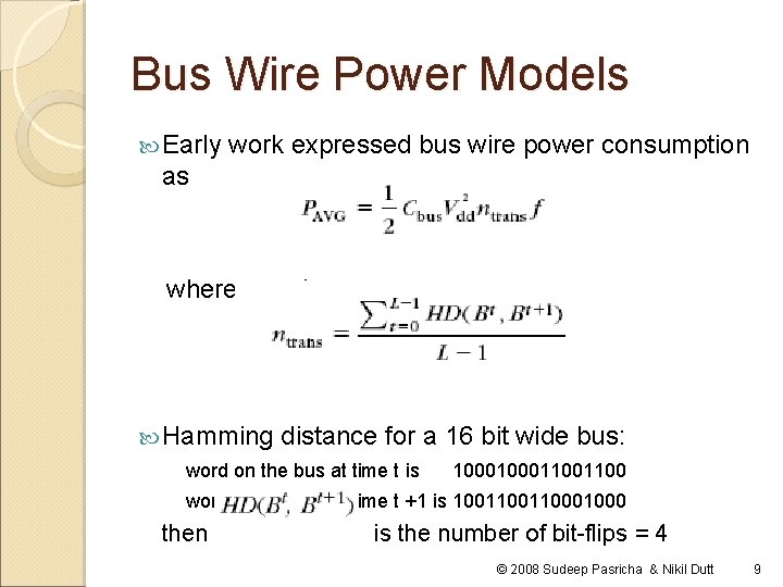
Bus Wire Power Models Early work expressed bus wire power consumption as where ntrans is Hamming distance for a 16 bit wide bus: word on the bus at time t is 10001100 word on the bus at time t +1 is 10011000 then is the number of bit-flips = 4 © 2008 Sudeep Pasricha & Nikil Dutt 9
![Bus Wire Power Models Chern et al EDL 92 proposed a model for Bus Wire Power Models Chern et al. [EDL ‘ 92] proposed a model for](https://slidetodoc.com/presentation_image_h2/165812980931d609cb385b23bab13772/image-10.jpg)
Bus Wire Power Models Chern et al. [EDL ‘ 92] proposed a model for wire capacitance ◦ three primary constituents of wire capacitance line-to-line capacitance line-to-ground capacitance crossover capacitance ◦ For wire on metal layer 2, © 2008 Sudeep Pasricha & Nikil Dutt 10

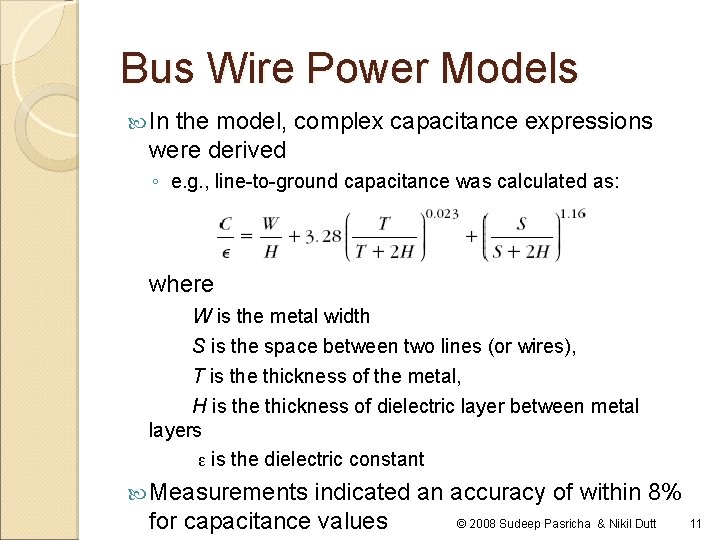
Bus Wire Power Models In the model, complex capacitance expressions were derived ◦ e. g. , line-to-ground capacitance was calculated as: where W is the metal width S is the space between two lines (or wires), T is the thickness of the metal, H is the thickness of dielectric layer between metal layers ɛ is the dielectric constant Measurements indicated an accuracy of within 8% © 2008 Sudeep Pasricha & Nikil Dutt for capacitance values 11
![Bus Wire Power Models More accurate analytical models Ho et al IEEE 2001 combine Bus Wire Power Models More accurate analytical models (Ho et al. [IEEE 2001]) combine](https://slidetodoc.com/presentation_image_h2/165812980931d609cb385b23bab13772/image-12.jpg)
Bus Wire Power Models More accurate analytical models (Ho et al. [IEEE 2001]) combine a bottom plate term with a fringing term ◦ to account for field lines originating from edge and top of wire Capacitance can then be modeled by four parallel plate capacitors for the top, bottom, left, and right sides, plus a constant term for fringing capacitance © 2008 Sudeep Pasricha & Nikil Dutt 12

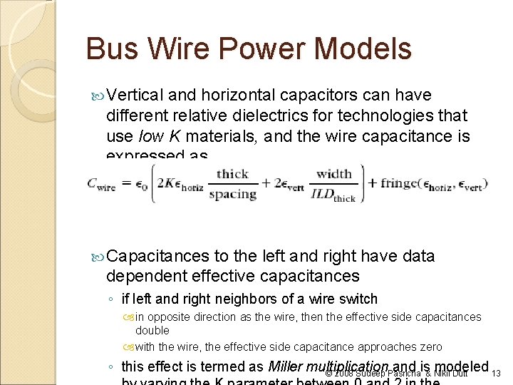
Bus Wire Power Models Vertical and horizontal capacitors can have different relative dielectrics for technologies that use low K materials, and the wire capacitance is expressed as Capacitances to the left and right have data dependent effective capacitances ◦ if left and right neighbors of a wire switch in opposite direction as the wire, then the effective side capacitances double with the wire, the effective side capacitance approaches zero ◦ this effect is termed as Miller multiplication and is modeled 13 © 2008 Sudeep Pasricha & Nikil Dutt

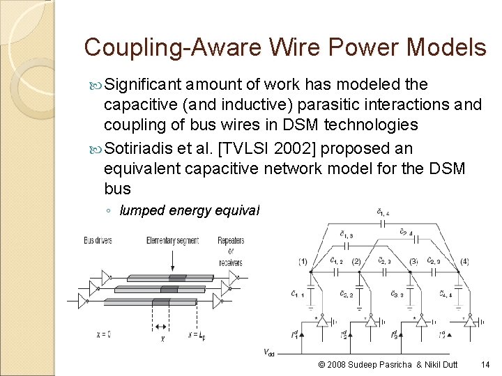
Coupling-Aware Wire Power Models Significant amount of work has modeled the capacitive (and inductive) parasitic interactions and coupling of bus wires in DSM technologies Sotiriadis et al. [TVLSI 2002] proposed an equivalent capacitive network model for the DSM bus ◦ lumped energy equivalent DSM bus model © 2008 Sudeep Pasricha & Nikil Dutt 14

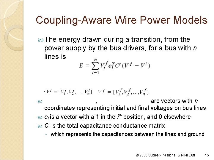
Coupling-Aware Wire Power Models The energy drawn during a transition, from the power supply by the bus drivers, for a bus with n lines is where , are vectors with n coordinates representing initial and final voltages on bus lines ei is a vector with a 1 in the ith position, and 0 elsewhere Ct is the total capacitance conductance matrix ◦ which represents the capacitances between the lines and ground © 2008 Sudeep Pasricha & Nikil Dutt 15

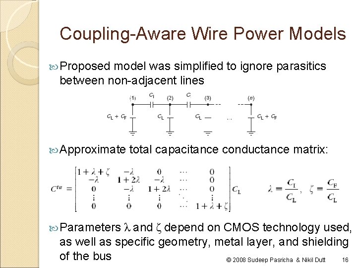
Coupling-Aware Wire Power Models Proposed model was simplified to ignore parasitics between non-adjacent lines Approximate Parameters total capacitance conductance matrix: λ and ζ depend on CMOS technology used, as well as specific geometry, metal layer, and shielding of the bus © 2008 Sudeep Pasricha & Nikil Dutt 16
![CouplingAware Wire Power Models Kretzschmar et al DATE 04 proposed an analytical model Coupling-Aware Wire Power Models Kretzschmar et al. [DATE ‘ 04] proposed an analytical model](https://slidetodoc.com/presentation_image_h2/165812980931d609cb385b23bab13772/image-17.jpg)
Coupling-Aware Wire Power Models Kretzschmar et al. [DATE ‘ 04] proposed an analytical model for power dissipation on a bus, accounting for repeaters Wire capacitance per unit length is © 2008 Sudeep Pasricha & Nikil Dutt 17

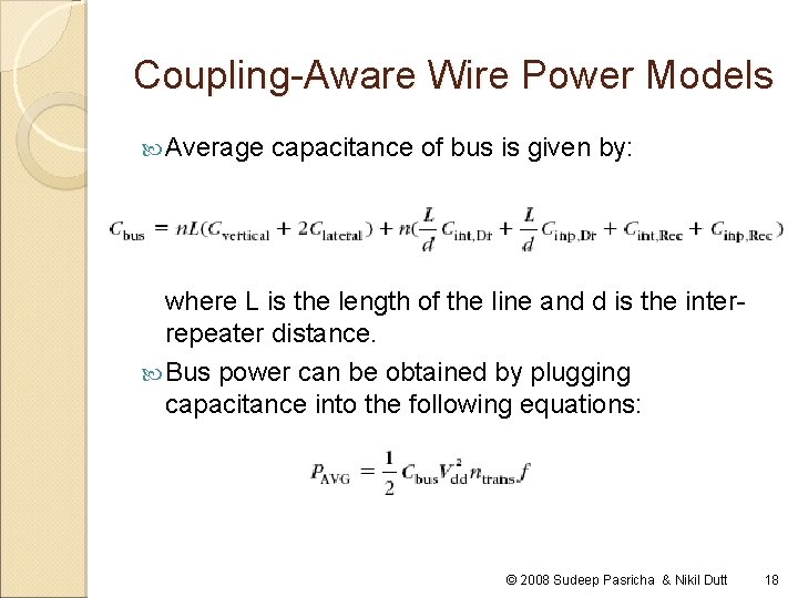
Coupling-Aware Wire Power Models Average capacitance of bus is given by: where L is the length of the line and d is the interrepeater distance. Bus power can be obtained by plugging capacitance into the following equations: © 2008 Sudeep Pasricha & Nikil Dutt 18
![CouplingAware Wire Power Models Gupta et al ICCAD 2003 proposed a bus power model Coupling-Aware Wire Power Models Gupta et al. [ICCAD 2003] proposed a bus power model](https://slidetodoc.com/presentation_image_h2/165812980931d609cb385b23bab13772/image-19.jpg)
Coupling-Aware Wire Power Models Gupta et al. [ICCAD 2003] proposed a bus power model for use in high level exploration Switching power PSW uses a table lookup technique ◦ low level transistor simulation used to construct a threewire lookup table for minimally spaced wires of various lengths ◦ gives power consumption for each type of transition in the transition set © 2008 Sudeep Pasricha & Nikil Dutt 19

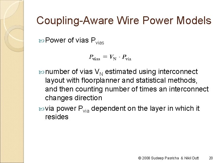
Coupling-Aware Wire Power Models Power of vias Pvias number of vias VN estimated using interconnect layout with floorplanner and statistical methods, and then counting number of times an interconnect changes direction via power Pvia dependent on the layer in which it resides © 2008 Sudeep Pasricha & Nikil Dutt 20

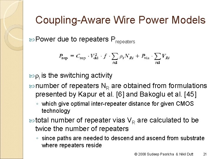
Coupling-Aware Wire Power Models Power due to repeaters Prepeaters ρi is the switching activity number of repeaters NR are obtained from formulations presented by Kapur et al. [6] and Bakoglu et al. [45] ◦ which give optimal inter-repeater distance for given CMOS technology total number of repeater vias VR are calculated to be twice the number of repeaters ◦ since paths are needed to descend ascend from substrate where repeaters reside © 2008 Sudeep Pasricha & Nikil Dutt 21

Outline Introduction Models for Power Estimation of Wires Models for Power Estimation of On-Chip Communication Architectures Models PVT for Thermal Estimation variation-aware Power Estimation © 2008 Sudeep Pasricha & Nikil Dutt 22

Power Estimation of On-Chip Communication Architectures In addition to wires, an important component of onchip communication architectures is bus logic Bridges, arbiters, decoders, buffer stages, etc. have a significant contribution towards on-chip power Important to account for power contribution for both bus logic and bus wires Especially true for increasingly complex communication architectures being used in multicore So. C designs today © 2008 Sudeep Pasricha & Nikil Dutt 23
![Power Estimation of OnChip Communication Architectures Lahiri et al CODESISSS 2004 proposed gate level Power Estimation of On-Chip Communication Architectures Lahiri et al. [CODES+ISSS 2004] proposed gate level](https://slidetodoc.com/presentation_image_h2/165812980931d609cb385b23bab13772/image-24.jpg)
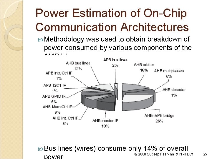
Power Estimation of On-Chip Communication Architectures Lahiri et al. [CODES+ISSS 2004] proposed gate level power estimation methodology for estimation of logic and bus wire power for AMBA AHB/APB © 2008 Sudeep Pasricha & Nikil Dutt 24

Power Estimation of On-Chip Communication Architectures Methodology was used to obtain breakdown of power consumed by various components of the AMBA bus Bus lines (wires) consume only 14% of overall © 2008 Sudeep Pasricha & Nikil Dutt 25
![Power Estimation of OnChip Communication Architectures Pasricha et al CODESISSS 2006 proposed an energy Power Estimation of On-Chip Communication Architectures Pasricha et al. [CODES+ISSS 2006] proposed an energy](https://slidetodoc.com/presentation_image_h2/165812980931d609cb385b23bab13772/image-26.jpg)
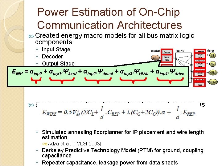
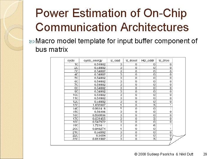
Power Estimation of On-Chip Communication Architectures Pasricha et al. [CODES+ISSS 2006] proposed an energy macro-model based methodology to estimate power for bus matrix communication architectures at the system-level An energy macro-model for a component has two basic elements ◦ variables – that represent factors (events) influencing energy consumption Control (e. g. signal value changes) Data (e. g. Hamming distance of input data values) Structural (e. g. bus widths) ◦ regression coefficients – that capture correlation between the variables and energy consumption Linear model © 2008 Sudeep Pasricha & Nikil Dutt 26

Power Estimation of On-Chip Communication Architectures Created energy macro-models for all bus matrix logic components ◦ Input Stage ◦ Decoder ◦ Output Stage ◦ Arbiter EINP = αinp 0 + αinp 1. Ψload + αinp 2. Ψdesel + αinp 3. ΨHDin + αinp 4. Ψdrive Energy consumption of wires at system-level, is given as ◦ Simulated annealing floorplanner for IP placement and wire length estimation Adya et al. [TVLSI 2003] ◦ Berkeley Predictive Technology Model (PTM) for ground, coupling capacitance ◦ Repeater capacitance, leakage power from data sheets

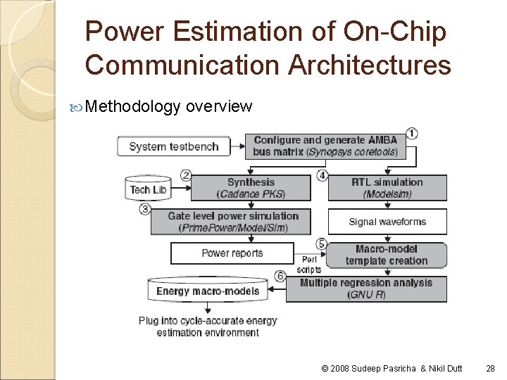
Power Estimation of On-Chip Communication Architectures Methodology overview © 2008 Sudeep Pasricha & Nikil Dutt 28

Power Estimation of On-Chip Communication Architectures Macro model template for input buffer component of bus matrix © 2008 Sudeep Pasricha & Nikil Dutt 29

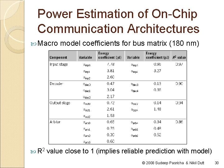
Power Estimation of On-Chip Communication Architectures Macro R 2 model coefficients for bus matrix (180 nm) value close to 1 (implies reliable prediction with model) © 2008 Sudeep Pasricha & Nikil Dutt 30

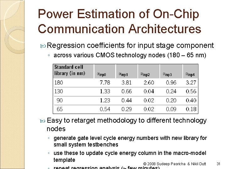
Power Estimation of On-Chip Communication Architectures Regression coefficients for input stage component ◦ across various CMOS technology nodes (180 – 65 nm) Easy to retarget methodology to different technology nodes ◦ generate gate level cycle energy numbers with new library for small system testbenches ◦ use these to update cycle energy column in the macro-model template © 2008 Sudeep Pasricha & Nikil Dutt 31

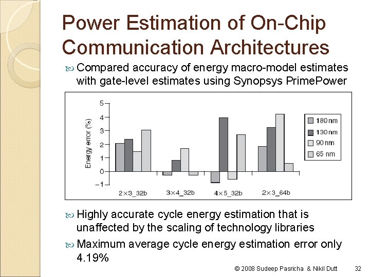
Power Estimation of On-Chip Communication Architectures Compared accuracy of energy macro-model estimates with gate-level estimates using Synopsys Prime. Power Highly accurate cycle energy estimation that is unaffected by the scaling of technology libraries Maximum average cycle energy estimation error only 4. 19% © 2008 Sudeep Pasricha & Nikil Dutt 32

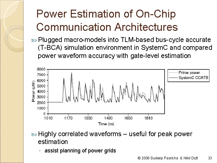
Power Estimation of On-Chip Communication Architectures Plugged macro-models into TLM-based bus-cycle accurate (T-BCA) simulation environment in System. C and compared power waveform accuracy with gate-level estimation Highly correlated waveforms – useful for peak power estimation ◦ assist planning of power grids © 2008 Sudeep Pasricha & Nikil Dutt 33

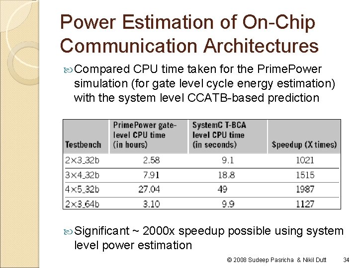
Power Estimation of On-Chip Communication Architectures Compared CPU time taken for the Prime. Power simulation (for gate level cycle energy estimation) with the system level CCATB-based prediction Significant ~ 2000 x speedup possible using system level power estimation © 2008 Sudeep Pasricha & Nikil Dutt 34
![Power Estimation of OnChip Communication Architectures Caldari et al DATE 2003 proposed energy macro Power Estimation of On-Chip Communication Architectures Caldari et al. [DATE 2003] proposed energy macro](https://slidetodoc.com/presentation_image_h2/165812980931d609cb385b23bab13772/image-35.jpg)
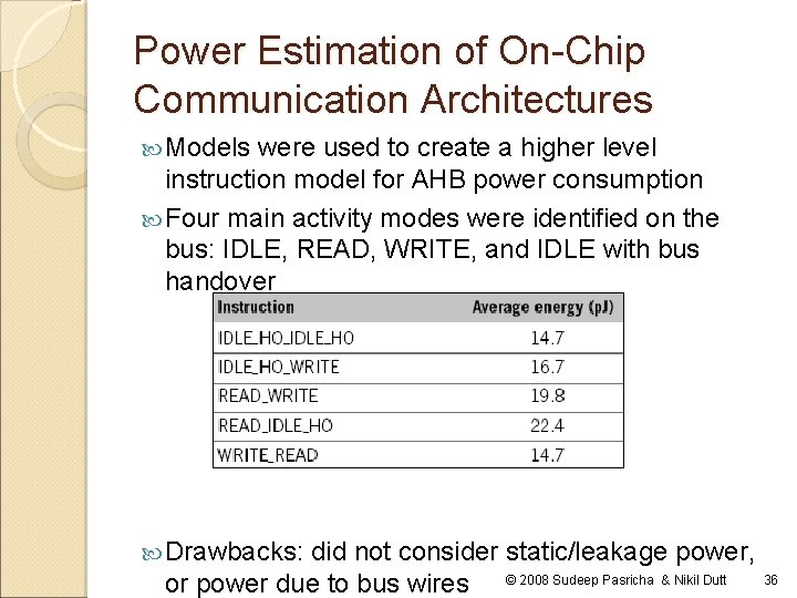
Power Estimation of On-Chip Communication Architectures Caldari et al. [DATE 2003] proposed energy macro models for an AMBA AHB bus Models created for arbiter, decoder, multiplexing logic ◦ For e. g. , decoder macro model where n 0 ≥ 2 is number of slaves attached to decoder n 1 is first integer number greater than log 2(n 0 -1) CO is capacitance of each output node © 2008 Sudeepof Pasricha Dutt 35 CPD is equivalent capacitance one& Nikil node

Power Estimation of On-Chip Communication Architectures Models were used to create a higher level instruction model for AHB power consumption Four main activity modes were identified on the bus: IDLE, READ, WRITE, and IDLE with bus handover Drawbacks: did not consider static/leakage power, or power due to bus wires © 2008 Sudeep Pasricha & Nikil Dutt 36
![Power Estimation of OnChip Communication Architectures Bona et al DATE 2004 proposed macromodels to Power Estimation of On-Chip Communication Architectures Bona et al. [DATE 2004] proposed macro-models to](https://slidetodoc.com/presentation_image_h2/165812980931d609cb385b23bab13772/image-37.jpg)
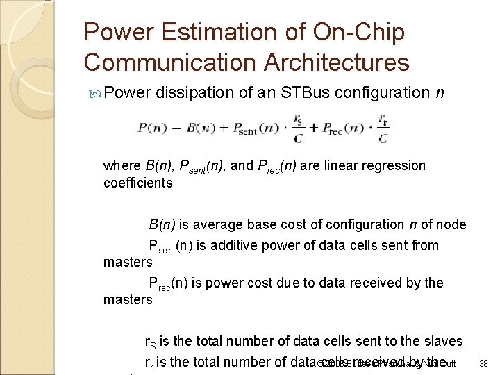
Power Estimation of On-Chip Communication Architectures Bona et al. [DATE 2004] proposed macro-models to estimate power consumption for the crossbar (or shared bus) topology-based Type 2 and Type 3 STBus Macro-model represents an STBus configuration n in design space S: where i is the number of initiators (or masters) t is the number of targets (or slaves) rqr, rpr are the no. of request or response resources, p is the type of arbitration policy, CL is the total output pin capacitance dps is the data path width (e. g. , 32 or 64 bits) © 2008 Sudeep Pasricha & Nikil Dutt 37

Power Estimation of On-Chip Communication Architectures Power dissipation of an STBus configuration n where B(n), Psent(n), and Prec(n) are linear regression coefficients B(n) is average base cost of configuration n of node Psent(n) is additive power of data cells sent from masters Prec(n) is power cost due to data received by the masters r. S is the total number of data cells sent to the slaves 2008 Sudeep Pasrichaby & Nikil rr is the total number of data ©cells received the. Dutt 38

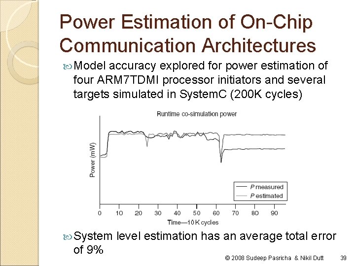
Power Estimation of On-Chip Communication Architectures Model accuracy explored for power estimation of four ARM 7 TDMI processor initiators and several targets simulated in System. C (200 K cycles) System of 9% level estimation has an average total error © 2008 Sudeep Pasricha & Nikil Dutt 39

Outline Introduction Models for Power Estimation of Wires Models for Power Estimation of On-Chip Communication Architectures Models PVT for Thermal Estimation variation-aware Power Estimation © 2008 Sudeep Pasricha & Nikil Dutt 40

Models for Thermal Estimation Thermal effects are an inseparable aspect of signal propagation ◦ Current flowing through an interconnect causes power dissipation Substrate, which is attached to the heat-sink, is typically far away from the interconnect lines (especially global-tier ones) ◦ heat generated by interconnect cannot be efficiently removed ◦ leads to increase in interconnect temperature -> Joule heating With aggressive CMOS scaling, low K inter-layer and intermetal dielectrics (IMDs) have been introduced ◦ to reduce RC delay, crosstalk, dynamic power consumption over Si. O 2 ◦ but low K dielectrics increase interconnect temperature have poor thermal conductivities Increasing © 2008 Sudeep Pasricha & Nikil Dutt no. of metal layers (~6 in 180 nm to 10 in 50 nm) 41

Models for Thermal Estimation Thermal effects have a significant impact on the performance, power, design, and reliability of interconnects because: ◦ interconnect lifetime (or reliability) has an exponential dependence on the inverse metal temperature ◦ thermal effects put a limit on maximum allowed root mean square (RMS) current density through the interconnects ◦ interconnect metal resistivity is dependent on temperature e. g. , resistivity of Cu increases by 39% from 20°C to 120°C higher resistivity causes larger RC delay that degrades performance ◦ leakage power has a significant dependence on temperature, and can be order of magnitudes greater at high temperatures ◦ thermally induced open circuit metal failure under short duration high peak currents including electrostatic discharge (ESD) can introduce latent electromagnetic (EM) damage ESD is the single largest cause of failures ICs. Pasricha © 2008 in Sudeep & Nikil Dutt 42
![Models for Thermal Estimation Sotiriadis et al TVLSI 2002 proposed a model for the Models for Thermal Estimation Sotiriadis et al. [TVLSI 2002] proposed a model for the](https://slidetodoc.com/presentation_image_h2/165812980931d609cb385b23bab13772/image-43.jpg)
Models for Thermal Estimation Sotiriadis et al. [TVLSI 2002] proposed a model for the energy dissipated as heat on bus lines Energy drawn from the power supply consists of two parts: ◦ energy stored in the capacitances of the repeaters and bus ◦ energy dissipated as heat Energy drawn by the ith driver on a bus, which is converted into heat during a transition, is given by Total energy drawn from power supply Difference in energy stored in capacitances before and after switching © 2008 Sudeep Pasricha & Nikil Dutt 43

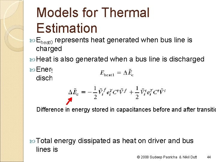
Models for Thermal Estimation Eheat 0 represents heat generated when bus line is charged Heat is also generated when a bus line is discharged Energy converted into heat during bus line discharging is: Difference in energy stored in capacitances before and after transitio Total energy dissipated as heat on driver and bus lines is © 2008 Sudeep Pasricha & Nikil Dutt 44
![Models for Thermal Estimation Sundaresan et al VLSID 2005 proposed anothermal model for bus Models for Thermal Estimation Sundaresan et al. [VLSID 2005] proposed anothermal model for bus](https://slidetodoc.com/presentation_image_h2/165812980931d609cb385b23bab13772/image-45.jpg)
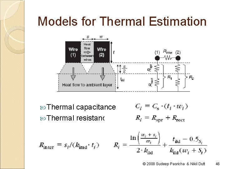
Models for Thermal Estimation Sundaresan et al. [VLSID 2005] proposed anothermal model for bus lines Created equivalent electrical and thermal RC network for a 5 bit bus © 2008 Sudeep Pasricha & Nikil Dutt 45

Models for Thermal Estimation Thermal capacitance Thermal resistance © 2008 Sudeep Pasricha & Nikil Dutt 46

Outline Introduction Models for Power Estimation of Wires Models for Power Estimation of On-Chip Communication Architectures Models PVT for Thermal Estimation variation-aware Power Estimation © 2008 Sudeep Pasricha & Nikil Dutt 47

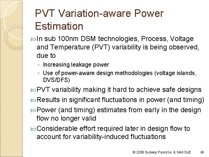
PVT Variation-aware Power Estimation In sub 100 nm DSM technologies, Process, Voltage and Temperature (PVT) variability is being observed, due to ◦ Increasing leakage power ◦ Use of power-aware design methodologies (voltage islands, DVS/DFS) PVT variability making it hard to achieve safe designs Results in significant fluctuations in power (and timing) Power (and timing) estimates from early in the design flow no longer valid Considerable effort required later in design flow to account for variability-induced fluctuations © 2008 Sudeep Pasricha & Nikil Dutt 48

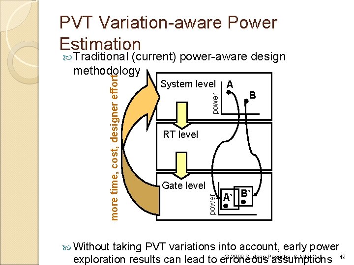
PVT Variation-aware Power Estimation (current) power-aware design methodology Without power System level A B RT level Gate level power more time, cost, designer effort Traditional A` B` taking PVT variations into account, early power © 2008 Sudeep Pasricha & Nikil Dutt exploration results can lead to erroneous assumptions 49
![PVT Variationaware Power Estimation Pasricha et al VLSID 2008 presented several experimental results to PVT Variation-aware Power Estimation Pasricha et al. [VLSID 2008] presented several experimental results to](https://slidetodoc.com/presentation_image_h2/165812980931d609cb385b23bab13772/image-50.jpg)
PVT Variation-aware Power Estimation Pasricha et al. [VLSID 2008] presented several experimental results to motivate PVT variation aware power estimation at the system-level Proposed system level PVT corner analysis for more accurate power characterization of comm. architectures ◦ PVT corners are library characterizations at design corners used by a foundry to communicate PVT variations to designers ◦ relate cell metrics (timing, power) to PVT variations Up until 130 nm design tools relied on three corners: ◦ Typical, Worst, and Best corners; +/- 20% variation among corners ◦ negligible leakage; Vdd major factor influencing power dissipation For sub-100 nm UDSM, many more corners required ◦ essential to analyze design across these corners © 2008 Sudeep Pasricha & Nikil Dutt 50

PVT Variation-aware Power Estimation Impact of PVT variation on power dissipation of AMBA AHB bus matrix at 90 nm Significant (as much as 10×) variation in power dissipation across PVT corners for on-chip comm. © 2008 Sudeep Pasricha & Nikil Dutt architectures 51

PVT Variation-aware Power Estimation Impact of PVT variation on power dissipation of AMBA AHB bus matrix at 65 nm Significant (as much as 10×) variation in power dissipation across PVT corners for on-chip comm. © 2008 Sudeep Pasricha & Nikil Dutt architectures 52

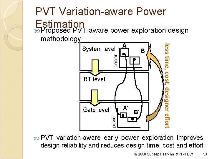
PVT Variation-aware Power Estimation Proposed PVT-aware power exploration design methodology A power B RT level A` power Gate level B` less time, cost, designer effort System level PVT variation-aware early power exploration improves design reliability and reduces design time, cost and effort © 2008 Sudeep Pasricha & Nikil Dutt 53

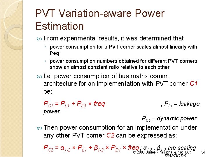
PVT Variation-aware Power Estimation From experimental results, it was determined that ◦ power consumption for a PVT corner scales almost linearly with freq ◦ power consumption numbers obtained for different PVT corners show an almost constant ratio relative to each other Let power consumption of bus matrix comm. architecture for an implementation with PVT corner C 1 be: PC 1 = PL 1 + PD 1 × freq ; PL 1 – leakage power PD 1 – dynamic power Then power consumption for an implementation under any other PVT corner C 2 can be expressed as: PC 2 = α 1 -2 × PL 1 + β 1 -2 × PD 1 × freq ; α 1 -2 , β 1 -2 are scaling © 2008 Sudeep Pasricha & Nikil Dutt 54

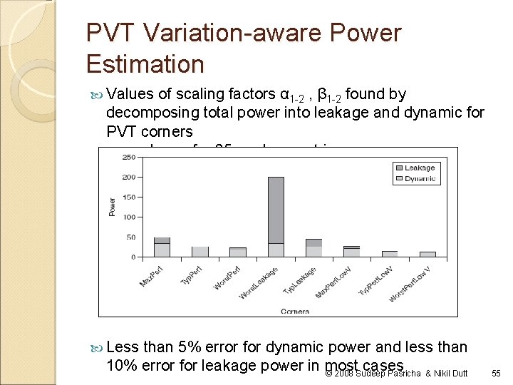
PVT Variation-aware Power Estimation Values of scaling factors α 1 -2 , β 1 -2 found by decomposing total power into leakage and dynamic for PVT corners ◦ as shown for 65 nm bus matrix case Less than 5% error for dynamic power and less than 10% error for leakage power in most cases © 2008 Sudeep Pasricha & Nikil Dutt 55

Summary Power is increasingly becoming a first class design objective ◦ thermal effects of power essential to consider in today’s designs Contribution of on-chip communication architectures to the overall chip power is rapidly increasing as technology scales ◦ critical need for accurate estimation models Presented ◦ ◦ an overview of several approaches to model power consumption of bus wires, power consumption of bus logic components thermal effects of signal propagation on interconnects PVT variations All of these models are most useful when incorporated into larger frameworks used for communication © 2008 Sudeep Pasricha & Nikil Dutt 56

© 2008 Sudeep Pasricha & Nikil Dutt 57