CMOS Devices PN junctions and diodes NMOS and


≈ gm/Cgs")


, m, ID, l, set Vo. Q at mid rail For high")


 vs VG is sensitive to VBS")

 has fixed shape")


- Slides: 64
CMOS Devices • • • PN junctions and diodes NMOS and PMOS transistors Resistors Capacitors Inductors Bipolar transistors
The MOS Transistors
The MOS Transistors
CMOS Device Model • Objective – Hand calculations for analog design – Non-idealities and their effects – Efficient and accurate simulation • CMOS transistor models – Large signal model – Small signal model – Simulation model – Noise model
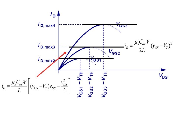
Good for VDS <VGS -VTH After that, ID become saturated.
Linear in deep triode Pro: voltage control of resistivity. Con: nonlinear resistor. As v. DS 0, ron
MOST Regions of Operation • Cut-off, or non-conducting: v. GS <VT – i. D=0 approximately • Conducting, or on: v. GS >=VT – Saturation: v. DS > v. GS – VT – Triode or linear or ohmic or non-saturation: v. DS <= v. GS – VT Saturation voltage:
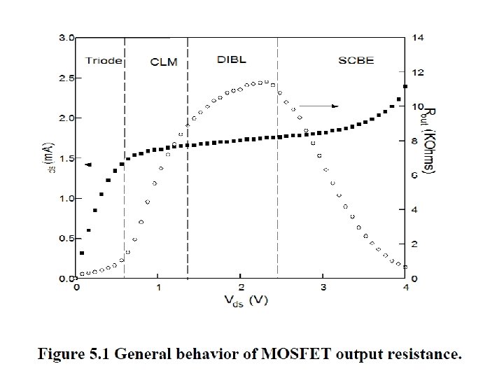
With channel length modulation
i. D vs v. DS for several VGS gds gm*DVGS
Influence of Channel Length on l Lmin = 0. 25 Johns and Martin book gives an approximate formula with l 1/L At >=2*Lmin, l is small, Ro is large After 1 um, l remains about the same
Influence of VBS changes threshold voltage, and hence changes i-v curve.
Temperature Dependence of Mobility Linear Temperature Dependence of threshold voltage Saturation Velocity Junction capacitance Barrier potential
This is nonlinear if Vbs is temperature dependent
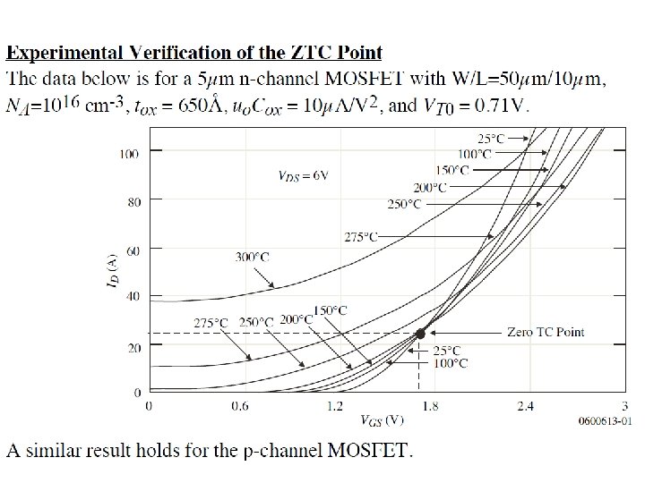
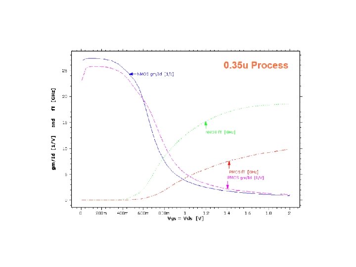
0. 35 um process ZTC biasing Referenced from Filanovsky’s paper
Reality: no single point crossing ID Not just one single crossing In AMI 0. 6 process Test on a single NMOS biased with fixed Vgs and Vds Vgs
AMI 0. 6 To refine the value. Vgs=1. 12 V Vgs=1. 14 V Optimum curve TC = 41 ppm/C Vgs=1. 17 V
Generic 018 Vgs=0. 717 V TC=27 ppm/C Vgs=0. 721 V Vgs=0. 727 V
Large signal model for approximate hand caculation
Capacitors Of The MOSFET
Capacitors in Cutoff
Capacitors in Saturation
Capacitors in Triode
Small signal model
Typically: VDB, VSB are in such a way that there is a reversely biased pn junction. Therefore: gbd ≈ gbs ≈ 0
In saturation: But
Intrinsic DC voltage gain: gm/gds = gm*rds
In non-saturation region
Intrinsic gain For large gain, use small ID or small over drive voltage, or in moderate to weak inversion.
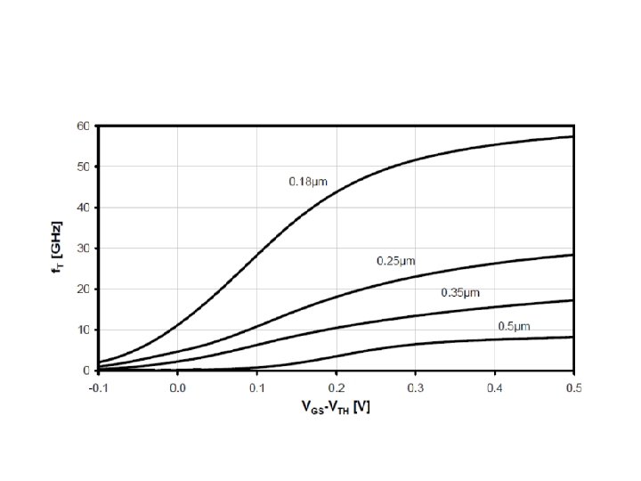
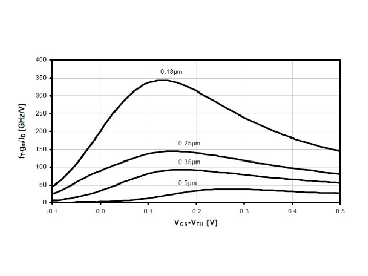
High Frequency Figure of Merit w. T • • • AC current source input to G AC short S, D, B to gnd (i. e. constant voltages) Measure AC drain current output Calculate current gain Find frequency at which current gain = 1. Ignore rs and rd, Cbs, Cbd, gds, gbd all have zero voltage drop and hence zero current • Vgs = Iin /jw(Cgs+Cgb+Cgd) ≈ Iin /jw(Cgs+Cgd) • Io = − (gm − jw. Cgd)Vgs ≈ − gm Iin /jw(Cgs+Cgd) • |Io/Iin| = |gm − jw. Cgd|/w(Cgs+Cgd) ≈ gm/w(Cgs+Cgd)
amplification |Io/Iin| 0 d. B attenuation w. T w
• At w. T, current gain =1 • w. T ≈ gm/(Cgs+Cgd)≈ gm/Cgs • or
For fastest operation, use Vod near but before f. T peak For power efficiency, use Vod before f. T corner
High Frequency Figures of Merit wmax • • AC current source input to G AC short S, B to gnd Measure AC power into the gate Assume complex conjugate load Compute max power delivered by the transistor Find maximum power gain Find frequency at which power gain = 1.
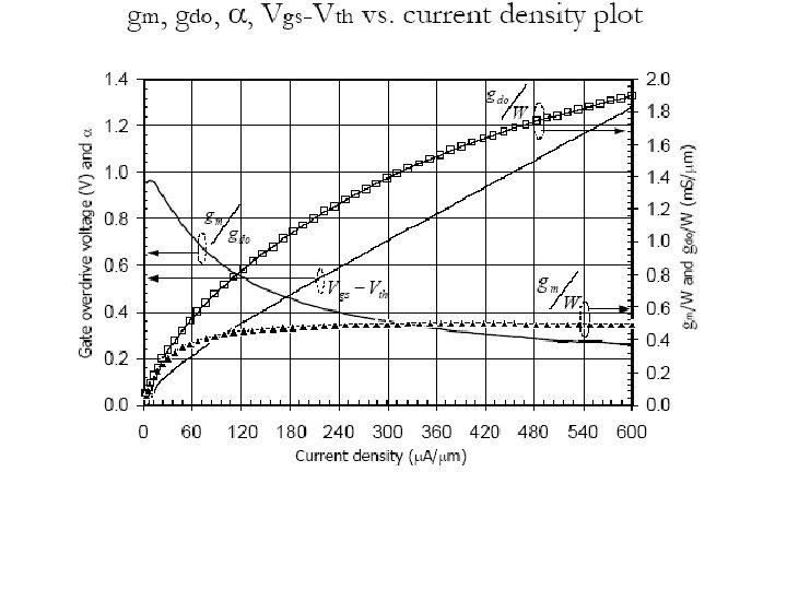
gdo vs gm in short channel
gdo vs gm in short channel
Insights: • gdo increases all the way with current density Iden • gm saturates when Iden larger than 100 m. A/mm – Velocity saturation, mobility degradation ---short channel effects – Low gm/current efficiency – High linearity • For power efficiency and gm efficiency – Use moderate to low current density – Use small over drive voltage
To Av: (W/L), m, ID, l, set Vo. Q at mid rail For high speed: Veff, m; L, Cgd, rg For better linearity: Vds, Vdb, set Vo. Q at mid rail Veff range: <~0. 5 V; or <~0. 3 V for efficiency ID/W range: <100 m. A/mm; or <40 m. A/mm for efficiency
Intrinsic voltage gain of MOSFET Sweep V 1 Measure vgs Intrinsic voltage gain = gm/go = Dvds/Dvgs for constant Id
Weak inversion • When VGS is reduced to Vth, the drain current does not go to zero – It does not follow square law – It does not follow exponential law • When VGS is markedly below Vth, the drain current becomes an exponential function of VGS. – Behaves very much like a diode
A model from weak to strong inv
In strong inversion, n is about 1
In weak inversion
In weak inversion If vt = 25 m. V, n=2, gm/ID = 20 n=1. 5, gm/ID = 27 n=1. 2, gm/ID = 33
ID vs VGS Exponential model Square law model simulation
ID/(W/L) vs VG is sensitive to VBS
gm/ID vs VG is also sensitive to VBS
But gm/ID vs ID/(W/L) has fixed shape
Related VDD insensitive circuits • Filanovsky, etc, “Mutual Compensation of Mobility and Threshold Voltage Temperature Effects with Applications in CMOS Circuits”. • G. Giustolisi “A Low-Voltage Low-Power Voltage Reference Based on Subthreshold MOSFETs”. • Ka Nang Leung “A CMOS Voltage Reference Based on Weighted VGS for CMOS Low-Dropout Linear Regulators”. • Bernhard Boser. “Analog Circuit Design with Submicron Transistors". IEEE SSCS Meeting, Santa Clara Valley, May 2005.
TSMC 0. 18 um Process
TSMC 0. 18 um Process
TSMC 0. 18 um Process
TSMC 0. 18 um Process
TSMC 0. 18 um Process
TSMC 0. 18 um Process