CMOS Devices PN junctions and diodes NMOS and


=638")


- Slides: 36
CMOS Devices • • • PN junctions and diodes NMOS and PMOS transistors Resistors Capacitors Bipolar transistors
PN Junctions • • Diffusion causes depletion region D. R. is insulator and establishes barrier This leads to 1 -directional current flow Forms junction capacitor – Capacitance highly voltage dependent – Can be nuisance or benefits
PN Junctions
PN Junctions Initial impurity concentration
PN Junctions
PN Junctions
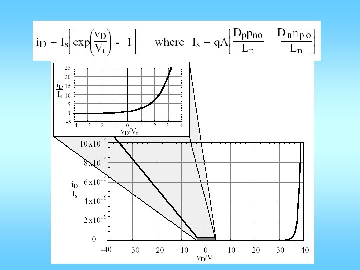
Example • NA=10^15 atoms/cm^3, ND=10^16, v. D=-10 • Ni=2. 25*10^20 • Phi_o=26 ln(10^15*10^16/2. 25/10^20)=638 m. V • xp= - 3. 5 mm • xn= 0. 35 mm • Max field = q*NA*xp/e = -5. 4*10^4 V/cm Note the large magnitude of the field
PN Junctions The depletion charge The junction capacitance
• Can be used as voltage controlled capacitor • Here m = 1/2 for the step change in impurity concentration. • For gradual concentration change, m = 1/3.
Impurity concentration profile for diffused pn junction
Current density at boundary due to wholes: Total: Diode current:
The MOS Transistor
TWO TYPES OF TRANSISTORS
CMOS Transistors
Capacitors • Two conductor plates separated by insulator for a capacitor • Intentional capacitors vs parasitic capacitors • Linear vs nonlinear capacitors Linear capacitors:
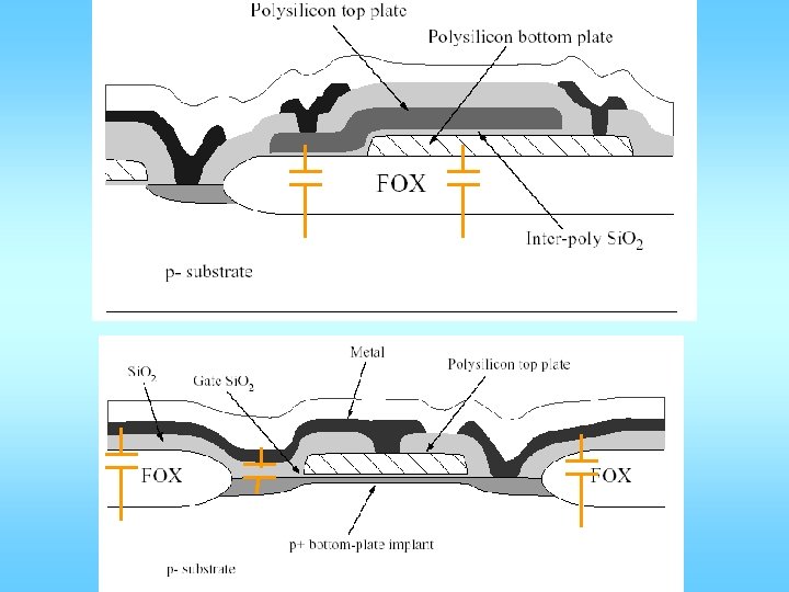
Integrated Capacitors in CMOS High density, good matching, but nonlinear
High density, good matching, good linearity, but require two-poly processes
Other Caps • • Cgs of enhancement transistors metal to poly metal to metal PN junction – diffusion to substrate – side wall • Fringe caps from top layer metals
Layering strategies
Parasitic Capacitors
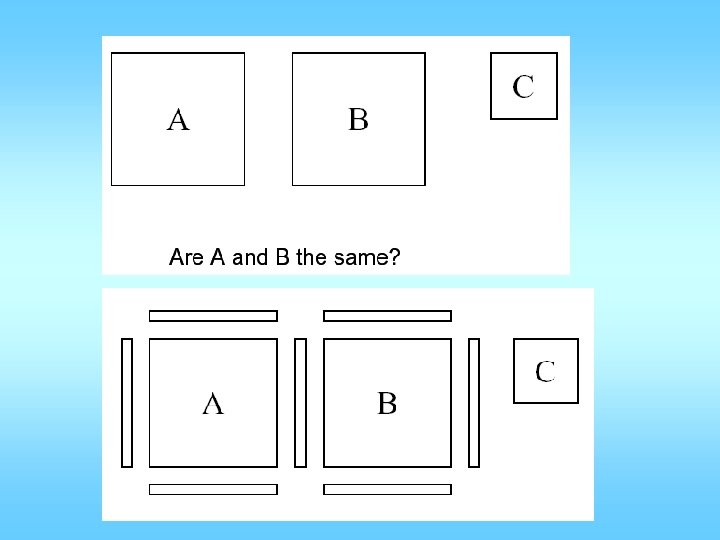
Proper layout of capacitors For achieving CA = 2 CB, which one is better?
Various Capacitor Errors
Resistors in CMOS • • • Diffusion resistor polysilicon resistor well resistor metal layer resistor contact resistor
Diffusion resistor in n-well
Polysilicon resistor on FOX
n-well resistor on p-substrate
Bipolar in CMOS PNP
Latch-up problem
Preventing Latch-up
ESD protection • A very serious problem • Not enough theoretical study • Many trade secrets • Learn from experienced designers
reset S 1 S R C Q D S 5 S R C Q D S 9 S R C Q D S 13 CLK S R C Q D S 16 S 2 S 12 S 6 R S C Q D S 8 R S C Q D S 4 R S C Q D S R C Q D S 10 S R C Q D S 14 S R C Q D S 15 S 3 S 11 S 7 R S C Q D S 3 R S C Q D S R C Q D S 11 S R C Q D S 15 S R C Q D S 14 S 10 S 8 R S C Q D S 6 R S C Q D S 2 R S C Q D S R C Q D S 12 S R C Q D S 16 S R C Q D S 13 R S C Q D S 9 R S C Q D S 5 R S C Q D S 1 R S C Q D