
Rocky K C Chang Version 0 1 14


- Slides: 50
Rocky K. C. Chang Version 0. 1, 14 October 2017
§ Have a basic understanding of how transistors are used to implement the basic logic gates. § Know how to obtain Boolean function and logic circuit for a given truth table. § Know how to simplify a Boolean function by applying various Boolean laws. § Know how to simplify a Boolean function by the Karnaugh map. 2
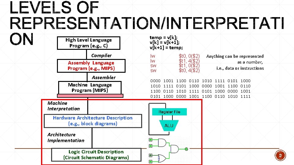
High Level Language Program (e. g. , C) Compiler Assembly Language Program (e. g. , MIPS) Assembler Machine Language Program (MIPS) temp = v[k]; v[k] = v[k+1]; v[k+1] = temp; lw lw sw sw 0000 1010 1100 0101 $t 0, 0($2) $t 1, 4($2) $t 1, 0($2) $t 0, 4($2) 1001 1111 0110 1000 1100 0101 1010 0000 0110 1000 1111 1001 Anything can be represented as a number, i. e. , data or instructions 1010 0000 0101 1100 1111 1000 0110 0101 1100 0000 1010 1000 0110 1001 1111 Machine Interpretation Hardware Architecture Description (e. g. , block diagrams) Architecture Implementation Logic Circuit Description (Circuit Schematic Diagrams) 3
§ Every CS student should understand how a computer (not only a program) works. § But it is not necessary to know Verilog to design hardware and the nitty-gritty electronic stuff. § Every CS student should also understand the capabilities and limitations of hardware in general and processors in particular. § Every CS student should be able to evaluate the tradeoffs of different computing systems. 4
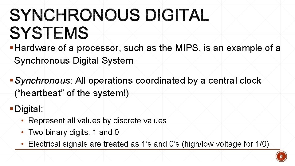
§ Hardware of a processor, such as the MIPS, is an example of a Synchronous Digital System § Synchronous: All operations coordinated by a central clock (“heartbeat” of the system!) § Digital: • Represent all values by discrete values • Two binary digits: 1 and 0 • Electrical signals are treated as 1’s and 0’s (high/low voltage for 1/0) 5
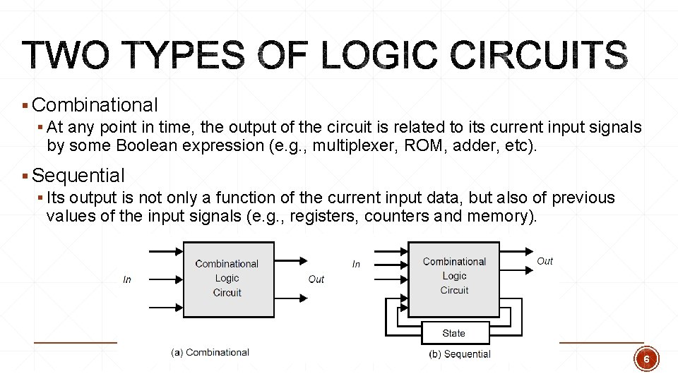
§ Combinational § At any point in time, the output of the circuit is related to its current input signals by some Boolean expression (e. g. , multiplexer, ROM, adder, etc). § Sequential § Its output is not only a function of the current input data, but also of previous values of the input signals (e. g. , registers, counters and memory). 6
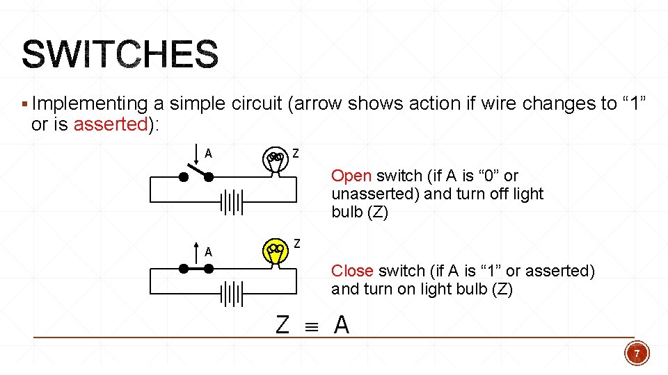
§ Implementing a simple circuit (arrow shows action if wire changes to “ 1” or is asserted): A Z Open switch (if A is “ 0” or unasserted) and turn off light bulb (Z) A Z Close switch (if A is “ 1” or asserted) and turn on light bulb (Z) Z A 7
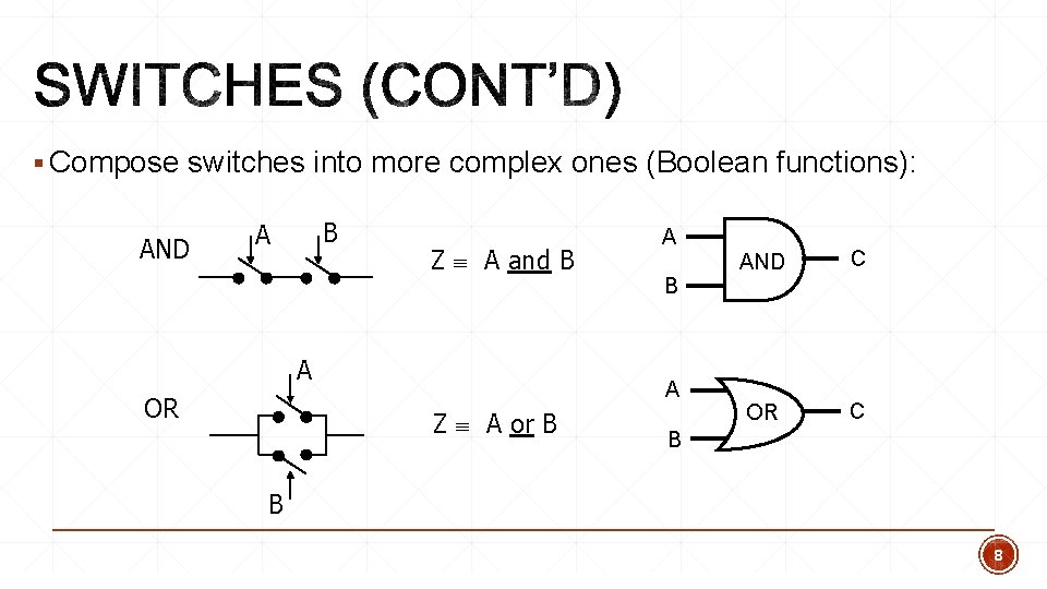
§ Compose switches into more complex ones (Boolean functions): AND B A Z A and B A OR A B A Z A or B AND C OR C B B 8
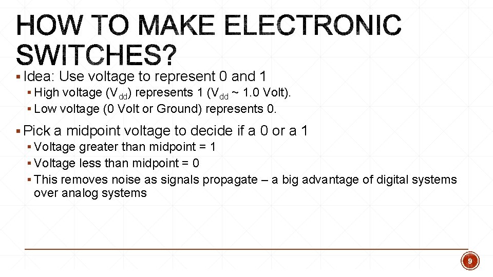
§ Idea: Use voltage to represent 0 and 1 § High voltage (Vdd) represents 1 (Vdd ~ 1. 0 Volt). § Low voltage (0 Volt or Ground) represents 0. § Pick a midpoint voltage to decide if a 0 or a 1 § Voltage greater than midpoint = 1 § Voltage less than midpoint = 0 § This removes noise as signals propagate – a big advantage of digital systems over analog systems 9
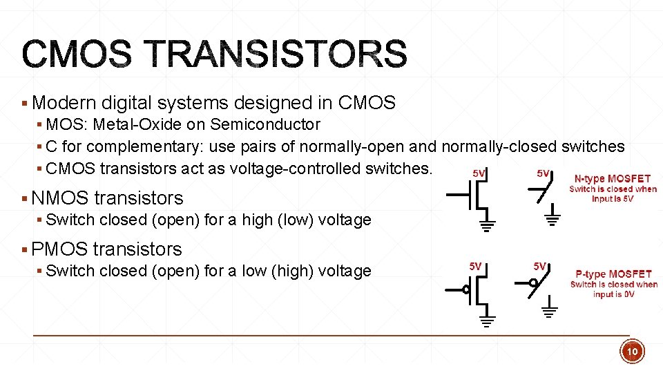
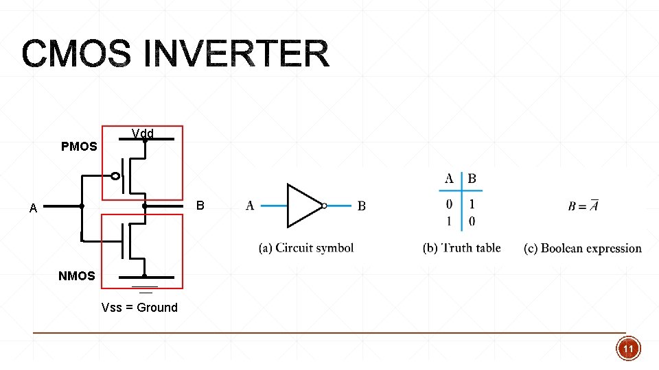
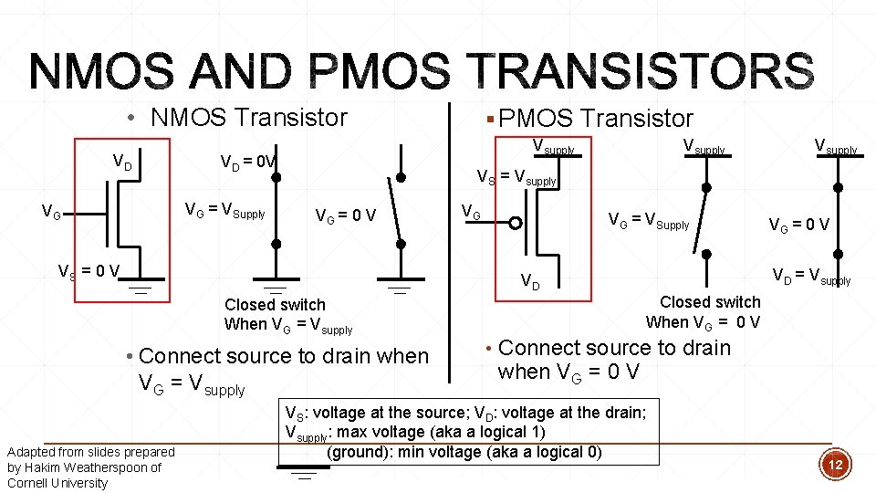
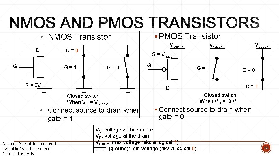
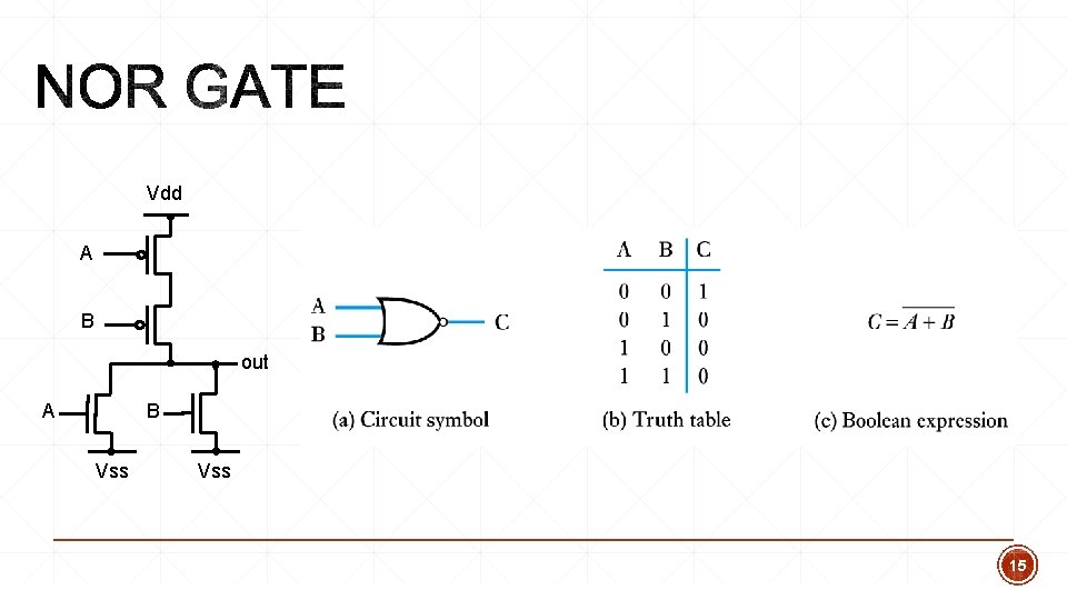
§ Modern digital systems designed in CMOS § MOS: Metal-Oxide on Semiconductor § C for complementary: use pairs of normally-open and normally-closed switches § CMOS transistors act as voltage-controlled switches. § NMOS transistors § Switch closed (open) for a high (low) voltage § PMOS transistors § Switch closed (open) for a low (high) voltage 10
PMOS Vdd B A NMOS Vss = Ground 11
• NMOS Transistor VD Vsupply VD = 0 V VG = VSupply VG § PMOS Transistor Vsupply VS = Vsupply VG = 0 V VS = 0 V VG VG = VSupply Closed switch When VG = Vsupply • Connect source to drain when VG = Vsupply VG = 0 V VD = Vsupply VD Adapted from slides prepared by Hakim Weatherspoon of Cornell University Vsupply Closed switch When VG = 0 V • Connect source to drain when VG = 0 V VS: voltage at the source; VD: voltage at the drain; Vsupply: max voltage (aka a logical 1) (ground): min voltage (aka a logical 0) 12
§ PMOS Transistor • NMOS Transistor D Vsupply D = 0 G G = 1 Vsupply S = Vsupply G = 0 S = 0 V G G = 1 • Connect source to drain when gate = 1 G = 0 D = 1 D Closed switch When VG = Vsupply Adapted from slides prepared by Hakim Weatherspoon of Cornell University Vsupply Closed switch When VG = 0 V § Connect source to drain when gate = 0 VS: voltage at the source VD: voltage at the drain Vsupply: max voltage (aka a logical 1) (ground): min voltage (aka a logical 0) 13
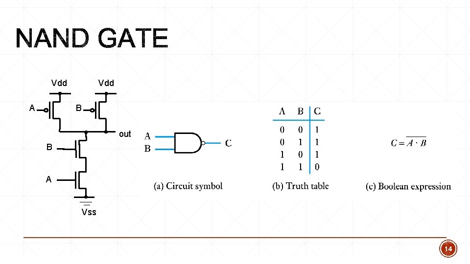
Vdd A Vdd B out B A Vss 14
Vdd A B out B A Vss 15
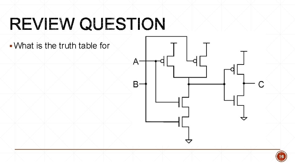
§ What is the truth table for 16
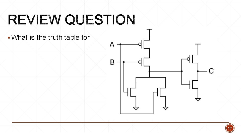
§ What is the truth table for 17
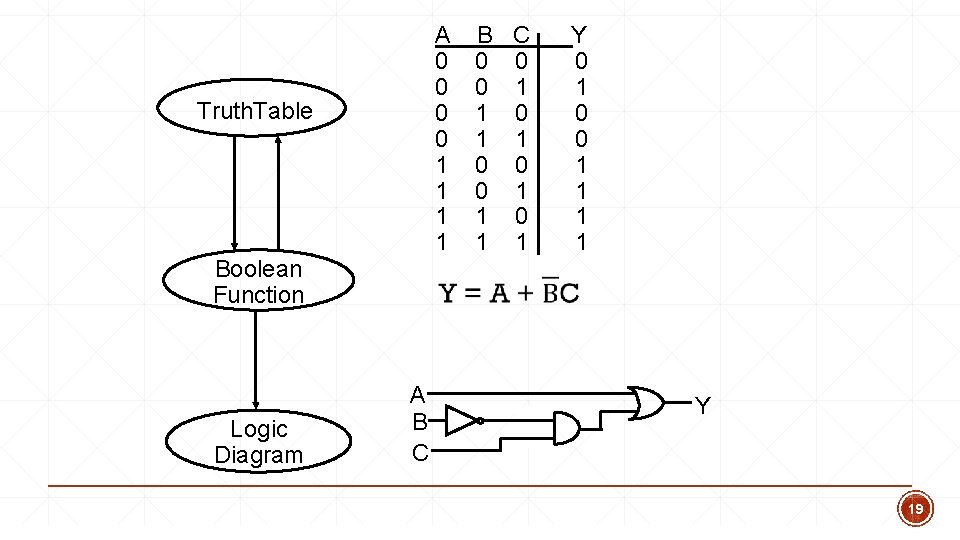
§ Question: How to design a logic circuit to obtain the desired output from given inputs? § We will need § Truth table (specifying the desired output for each input) § Boolean function (expressing the output in terms of the input) § Boolean algebra (used for deriving a Boolean function from a truth table) § Basic logic gates (implementing a Boolean function) 18
A B C Y 0 0 1 1 0 1 0 0 0 1 1 0 0 1 1 0 1 1 1 Truth. Table Boolean Function Logic Diagram A B C Y 19
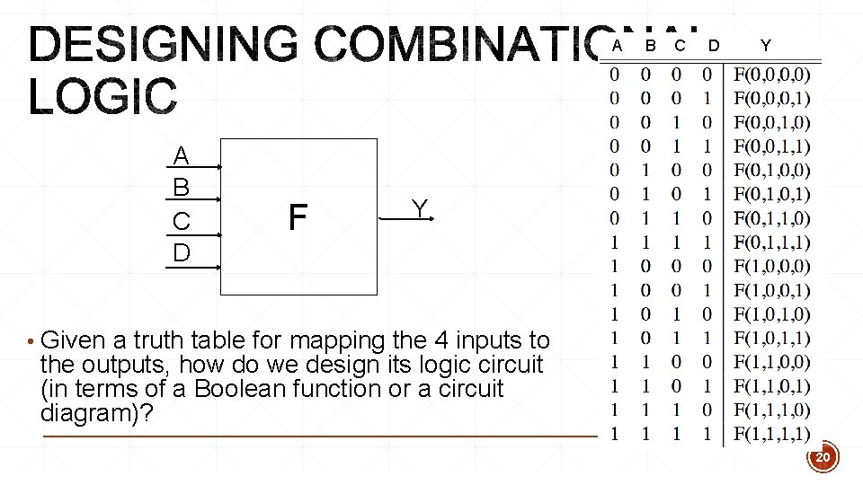
A B C D Y A B C D F Y • Given a truth table for mapping the 4 inputs to the outputs, how do we design its logic circuit (in terms of a Boolean function or a circuit diagram)? 20
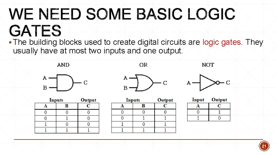
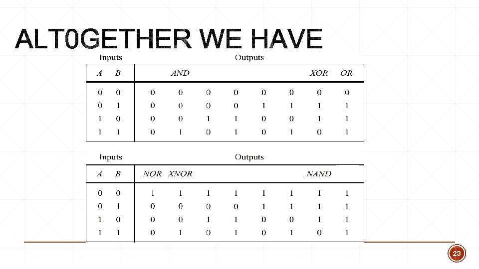
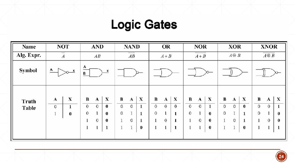
§ The building blocks used to create digital circuits are logic gates. They usually have at most two inputs and one output. 21
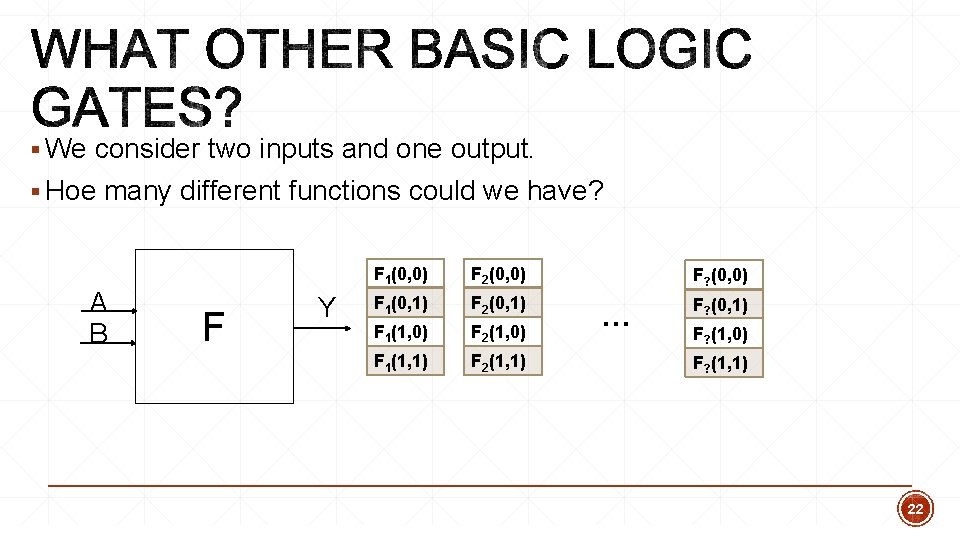
§ We consider two inputs and one output. § Hoe many different functions could we have? A B F Y F 1(0, 0) F 2(0, 0) F? (0, 0) F 1(0, 1) F 2(0, 1) F? (0, 1) F 1(1, 0) F 2(1, 0) F 1(1, 1) F 2(1, 1) … F? (1, 0) F? (1, 1) 22
23
24
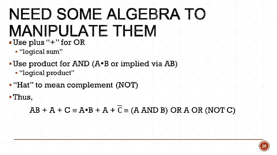
§ 25
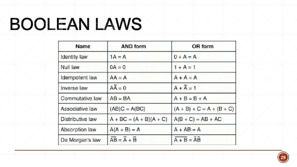
26
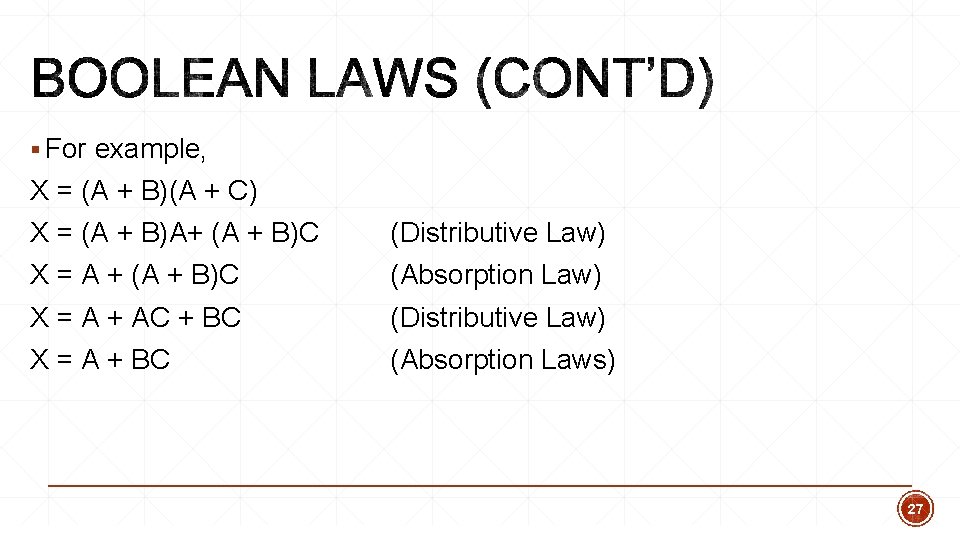
§ For example, X = (A + B)(A + C) X = (A + B)A+ (A + B)C (Distributive Law) X = A + (A + B)C (Absorption Law) X = A + AC + BC (Distributive Law) X = A + BC (Absorption Laws) 27
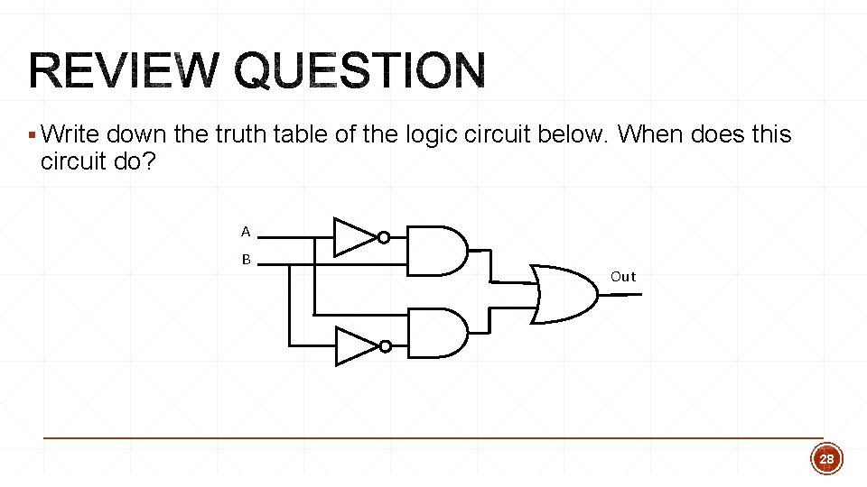
§ Write down the truth table of the logic circuit below. When does this circuit do? A B Out 28
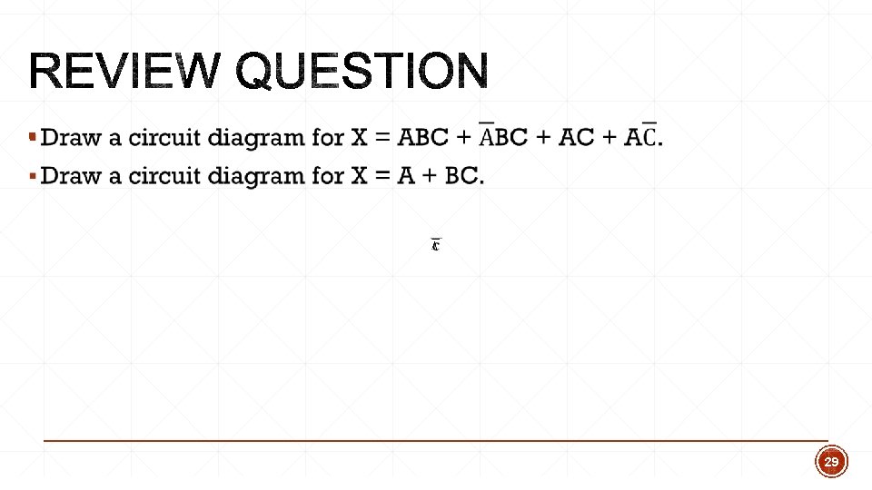
§ 29
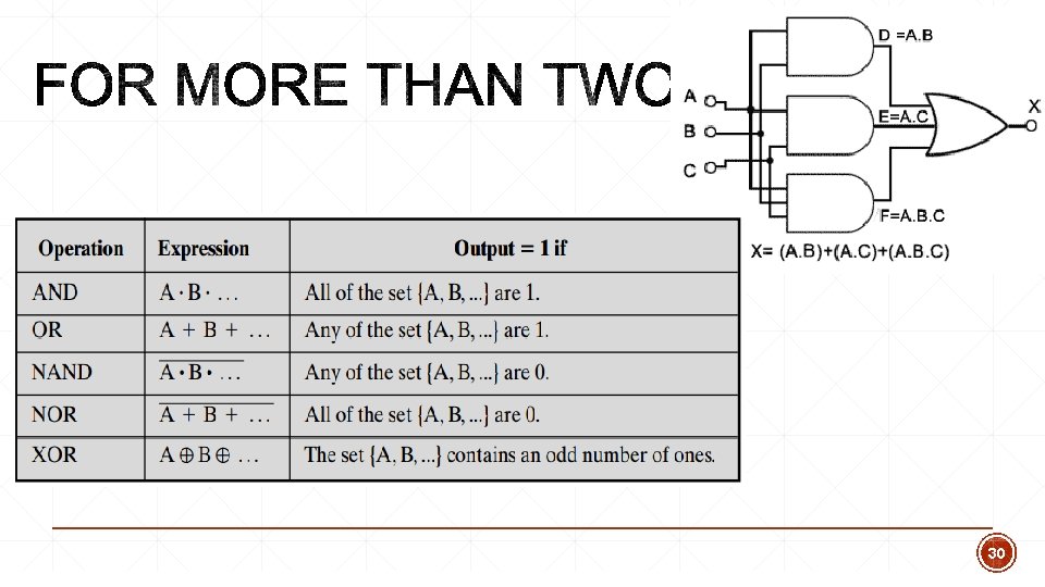
30
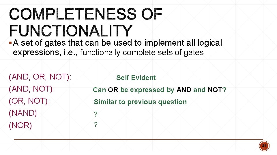
§ A set of gates that can be used to implement all logical expressions, i. e. , functionally complete sets of gates (AND, OR, NOT): Self Evident (AND, NOT): Can OR be expressed by AND and NOT? (OR, NOT): Similar to previous question (NAND) ? ? (NOR) 31
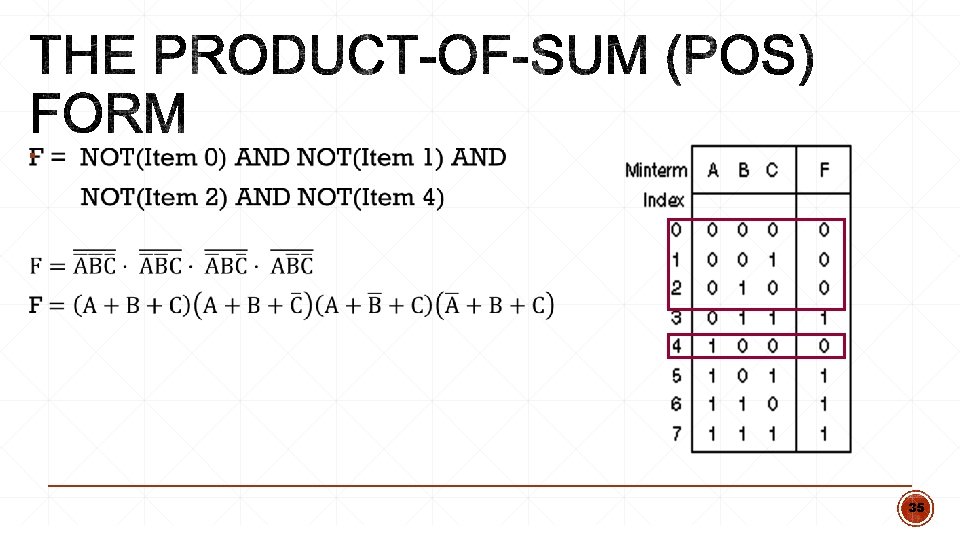
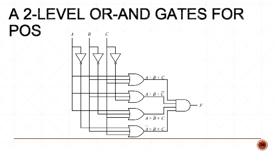
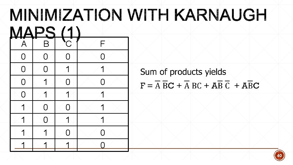
§ Problem: Given a truth table of a desired function, how to derive its Boolean function/logic circuit? § Sum of products § Product of sum § Karnaugh Map (K-map) to simplify the circuit 32
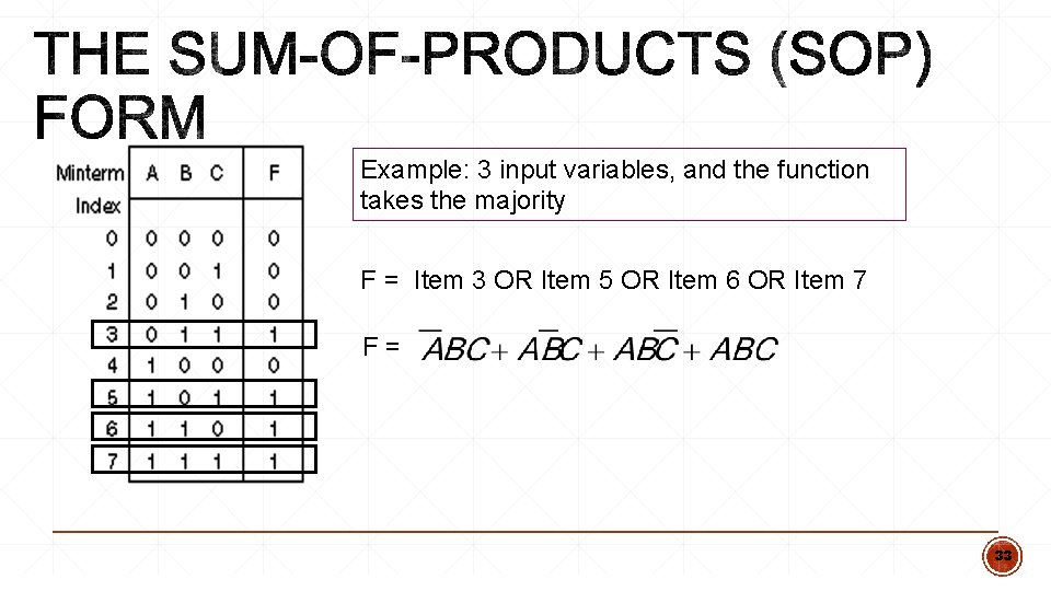
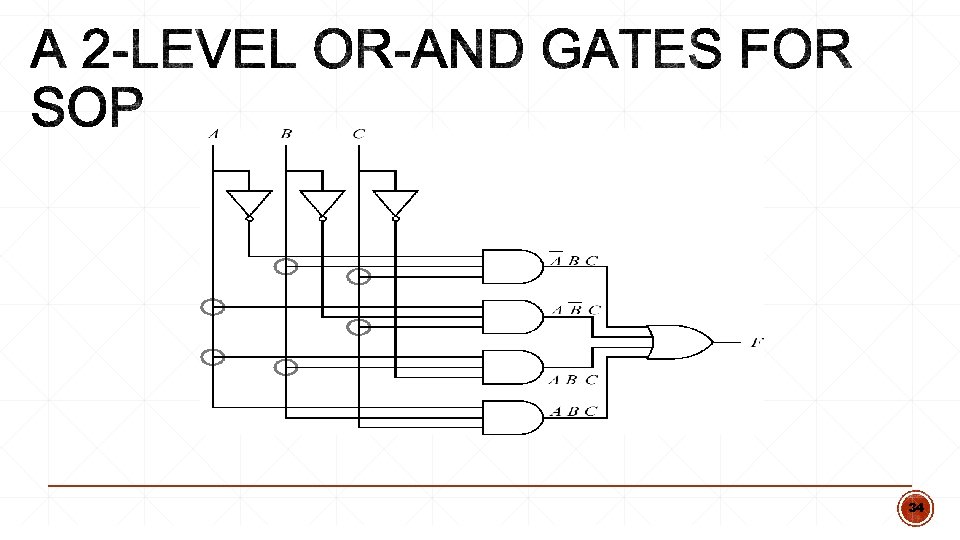
Example: 3 input variables, and the function takes the majority F = Item 3 OR Item 5 OR Item 6 OR Item 7 F = 33
34
§ 35
36
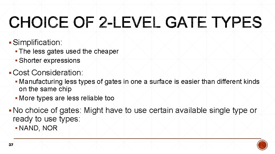
§ Simplification: § The less gates used the cheaper § Shorter expressions § Cost Consideration: § Manufacturing less types of gates in one a surface is easier than different kinds on the same chip § More types are less reliable too § No choice of gates: Might have to use certain available single type or ready to use types: § NAND, NOR 37
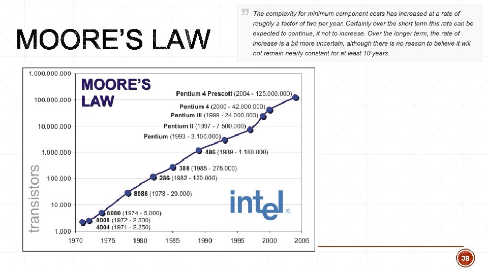
38
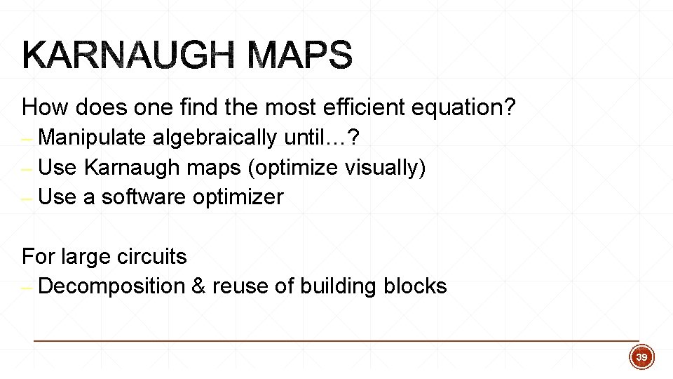
How does one find the most efficient equation? – Manipulate algebraically until…? – Use Karnaugh maps (optimize visually) – Use a software optimizer For large circuits – Decomposition & reuse of building blocks 39
A 0 0 1 1 B 0 0 1 1 C 0 1 0 1 F 0 1 1 1 0 0 40
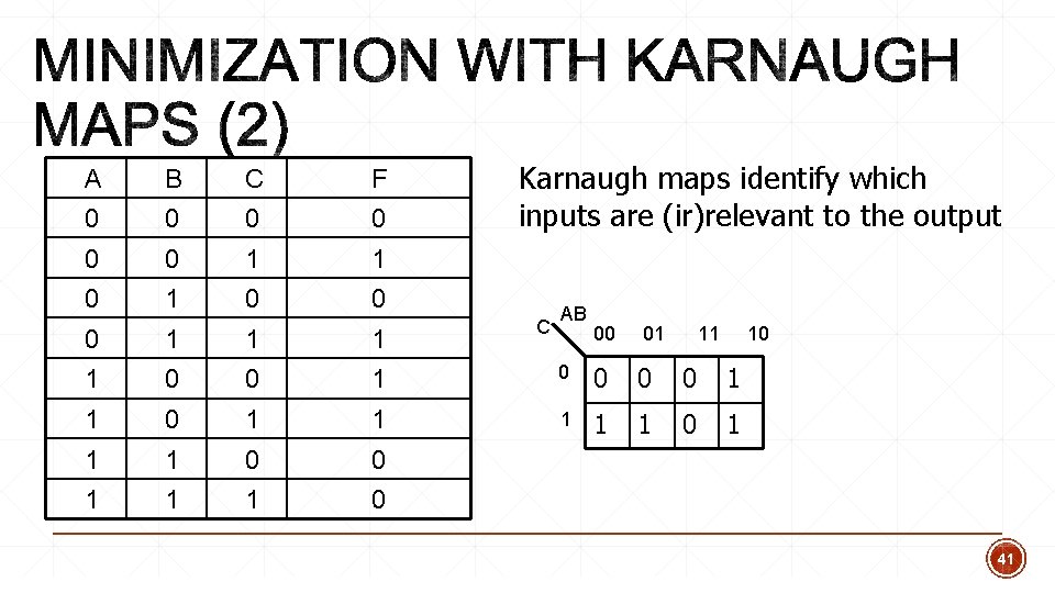
A B C F 0 0 0 1 1 0 0 Karnaugh maps identify which inputs are (ir)relevant to the output C AB 00 01 11 10 0 1 1 0 0 1 1 0 1 1 1 0 41
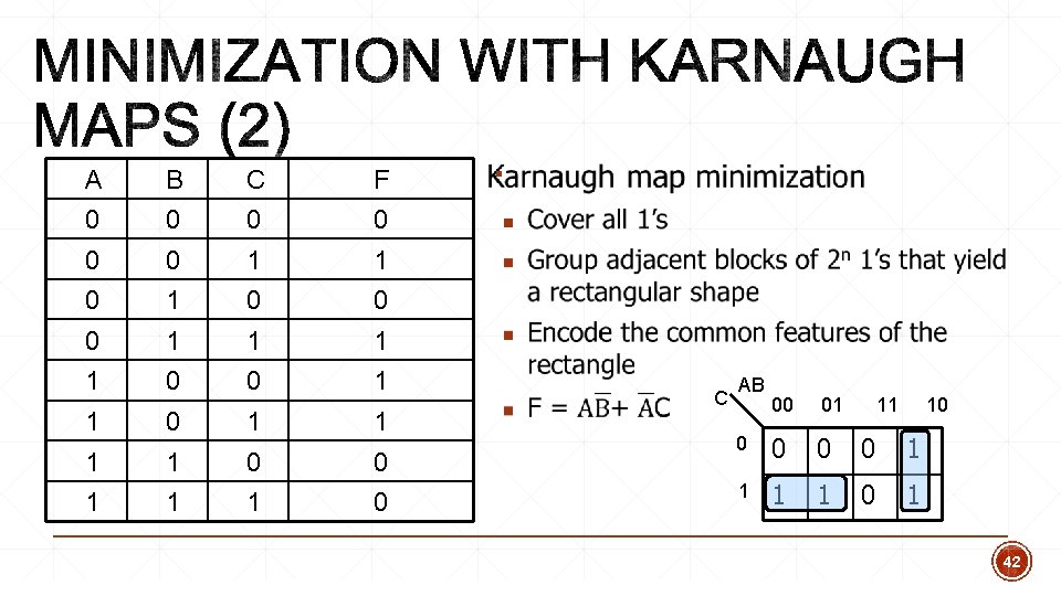
A B C F 0 0 0 1 1 1 1 0 0 1 1 1 0 § C AB 00 01 11 10 0 0 1 1 0 1 42
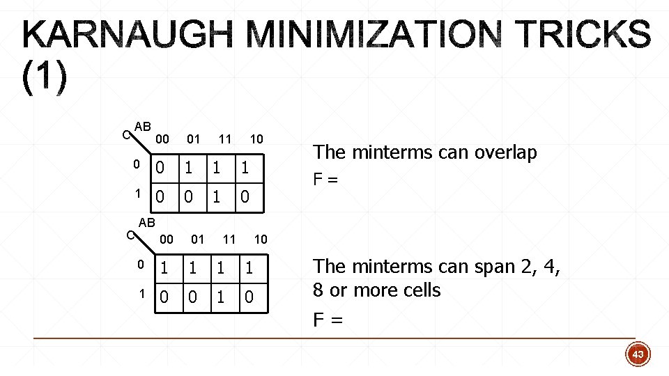
C AB 00 01 11 10 0 0 1 1 0 0 1 0 C The minterms can overlap F= AB 00 01 11 10 0 1 1 1 0 0 1 0 The minterms can span 2, 4, 8 or more cells F= 43
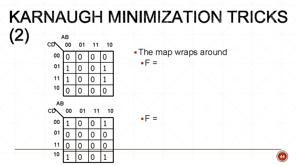
AB 00 01 11 10 CD 00 0 0 01 1 0 0 1 10 0 0 § The map wraps around § F = AB CD 00 01 11 10 00 1 01 0 0 0 0 10 1 0 0 1 § F = 44
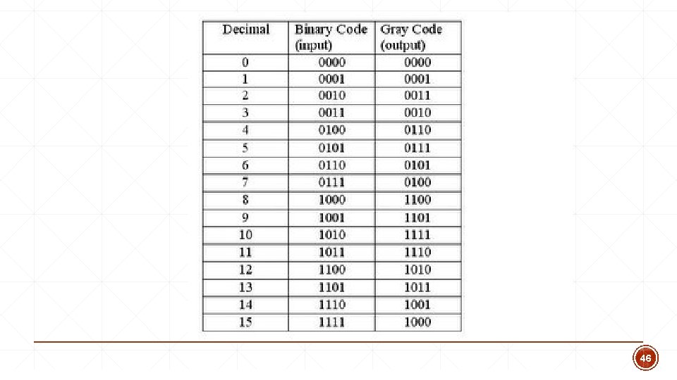
§ Consider the table on the next page for converting binary coded decimal (BCD) to Gray Code. Apply SOP and K-map to obtain the Boolean functions for G 0, G 1, G 2, and G 3. 45
46
§ Digital circuits are built from a small number of gates, or even a single type of gates. § The gates can be built by two types of CMOS transistors which serve as voltage-driven switches. § Sum of products or products of sum can be used to obtain Boolean function from a given truth table. § K-map can be applied to reduce the number of gates required to implement a truth table. 47
§ Read B 1 -B 3 in David Patterson and John Hennessy, Computer Organization and Design, 5 th edition, Morgan Kaufmann, 2014. § Read 11. 1 -11. 3 in William Stallings, Computer organization and architecture: Designing for performance, 9 th edition, Prentice Hall, 2013. 48
§ This set of slides are prepared mainly based on § The slides prepared by K. Asanovic & V. Stojanovic for CS 61 C at UC/Berkeley (http: //inst. eecs. Berkeley. edu/~cs 61 c/sp 15) § Prof. Qin Lu’s slides from http: //www 4. comp. polyu. edu. hk/~csluqin/comp 2421/ 49