Silicon Vertex Tracker RD towards the Technical Design

- Slides: 35

Silicon Vertex Tracker R&D towards the Technical Design Report Giuliana Rizzo INFN and University, Pisa on behalf of SVT-Super. B group • The SVT in the CDR • From CDR to TDR • Main Goals of the R&D Super. B Detector R&D Workshop G. Rizzo SLAC February 14 -16 2008 SLACWorkshop February Super. B - SLAC 14 -16 Feb. 14, 2008 1

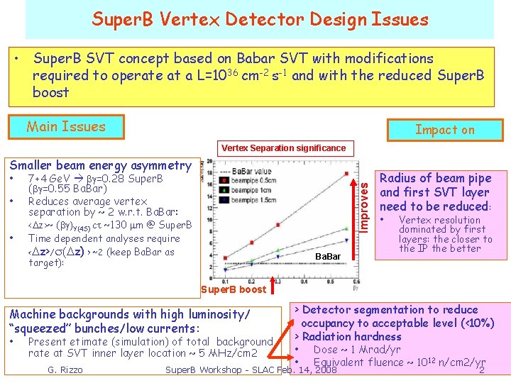
Super. B Vertex Detector Design Issues • Super. B SVT concept based on Babar SVT with modifications required to operate at a L=1036 cm-2 s-1 and with the reduced Super. B boost Main Issues Impact on Vertex Separation significance Smaller beam energy asymmetry • • 7+4 Ge. V bg=0. 28 Super. B (bg=0. 55 Ba. Bar) Reduces average vertex separation by ~ 2 w. r. t. Bar: Improves • <Dz>~ (bg)Y(4 S) ct ~130 mm @ Super. B Time dependent analyses require <Dz>/s(Dz) > ~2 (keep Ba. Bar as target): Ba. Bar Radius of beam pipe and first SVT layer need to be reduced: • Vertex resolution dominated by first layers: the closer to the IP the better Super. B boost Machine backgrounds with high luminosity/ “squeezed” bunches/low currents: • Present etimate (simulation) of total background rate at SVT inner layer location ~ 5 MHz/cm 2 G. Rizzo > Detector segmentation to reduce occupancy to acceptable level (<10%) > Radiation hardness • Dose ~ 1 Mrad/yr • Equivalent fluence ~ 1012 n/cm 2/yr Super. B Workshop - SLAC Feb. 14, 2008 2

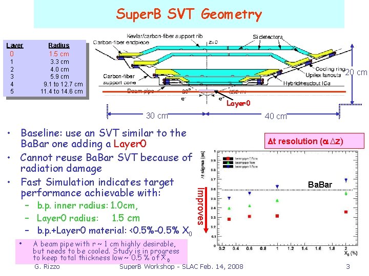
Super. B SVT Geometry Layer 0 Radius 1. 5 cm 1 2 3 4 5 3. 3 cm 4. 0 cm 5. 9 cm 9. 1 to 12. 7 cm 11. 4 to 14. 6 cm 20 cm Layer 0 30 cm – b. p. inner radius: 1. 0 cm, – Layer 0 radius: 1. 5 cm – b. p. +Layer 0 material: <0. 5%-0. 5% X 0 • A beam pipe with r ~ 1 cm highly desirable, but needs to be cooled. Study is in progress to keep total thickness low ~ 0. 5 % of X 0 G. Rizzo Dt resolution (a Dz) Improves • Baseline: use an SVT similar to the Ba. Bar one adding a Layer 0 • Cannot reuse Ba. Bar SVT because of radiation damage • Fast Simulation indicates target performance achievable with: 40 cm Super. B Workshop - SLAC Feb. 14, 2008 Ba. Bar 3

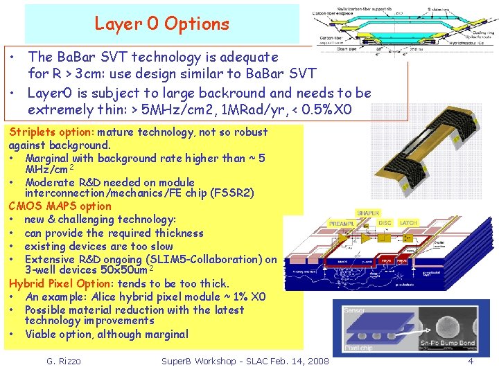
Layer 0 Options • The Ba. Bar SVT technology is adequate for R > 3 cm: use design similar to Ba. Bar SVT • Layer 0 is subject to large backround and needs to be extremely thin: > 5 MHz/cm 2, 1 MRad/yr, < 0. 5%X 0 Striplets option: mature technology, not so robust against background. • Marginal with background rate higher than ~ 5 MHz/cm 2 • Moderate R&D needed on module interconnection/mechanics/FE chip (FSSR 2) CMOS MAPS option • new & challenging technology: • can provide the required thickness • existing devices are too slow • Extensive R&D ongoing (SLIM 5 -Collaboration) on 3 -well devices 50 x 50 um 2 Hybrid Pixel Option: tends to be too thick. • An example: Alice hybrid pixel module ~ 1% X 0 • Possible material reduction with the latest technology improvements • Viable option, although marginal G. Rizzo Super. B Workshop - SLAC Feb. 14, 2008 4

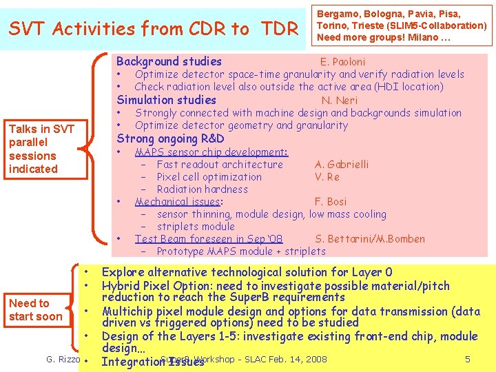
SVT Activities from CDR to TDR Bergamo, Bologna, Pavia, Pisa, Torino, Trieste (SLIM 5 -Collaboration) Need more groups! Milano … Background studies E. Paoloni • Optimize detector space-time granularity and verify radiation levels • Check radiation level also outside the active area (HDI location) Simulation studies N. Neri • Strongly connected with machine design and backgrounds simulation • Optimize detector geometry and granularity Talks in SVT parallel sessions indicated Strong ongoing R&D • • • Need to start soon • • G. Rizzo • MAPS sensor chip development: – Fast readout architecture A. Gabrielli – Pixel cell optimization V. Re – Radiation hardness Mechanical issues: F. Bosi – sensor thinning, module design, low mass cooling – striplets module Test Beam foreseen in Sep ‘ 08 S. Bettarini/M. Bomben – Prototype MAPS module + striplets Explore alternative technological solution for Layer 0 Hybrid Pixel Option: need to investigate possible material/pitch reduction to reach the Super. B requirements Multichip pixel module design and options for data transmission (data driven vs triggered options) need to be studied Design of the Layers 1 -5: investigate existing front-end chip, module design… Workshop - SLAC Feb. 14, 2008 5 Integration. Super. B Issues

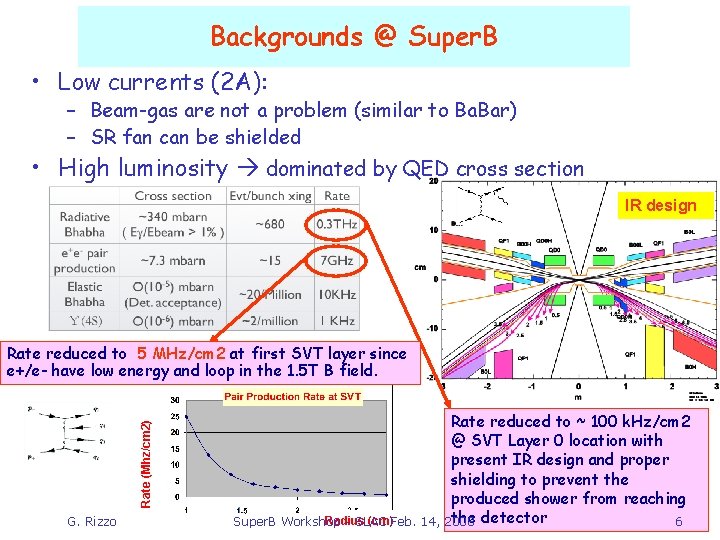
Backgrounds @ Super. B • Low currents (2 A): – Beam-gas are not a problem (similar to Ba. Bar) – SR fan can be shielded • High luminosity dominated by QED cross section IR design Rate (Mhz/cm 2) Rate reduced to 5 MHz/cm 2 at first SVT layer since e+/e- have low energy and loop in the 1. 5 T B field. G. Rizzo Rate reduced to ~ 100 k. Hz/cm 2 @ SVT Layer 0 location with present IR design and proper shielding to prevent the produced shower from reaching the detector Radius (cm)Feb. 14, 2008 Super. B Workshop - SLAC 6

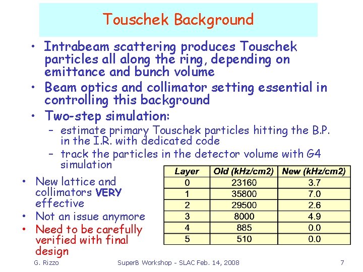
Touschek Background • Intrabeam scattering produces Touschek particles all along the ring, depending on emittance and bunch volume • Beam optics and collimator setting essential in controlling this background • Two-step simulation: – estimate primary Touschek particles hitting the B. P. in the I. R. with dedicated code – track the particles in the detector volume with G 4 simulation • New lattice and collimators VERY effective • Not an issue anymore • Need to be carefully verified with final design G. Rizzo Super. B Workshop - SLAC Feb. 14, 2008 7

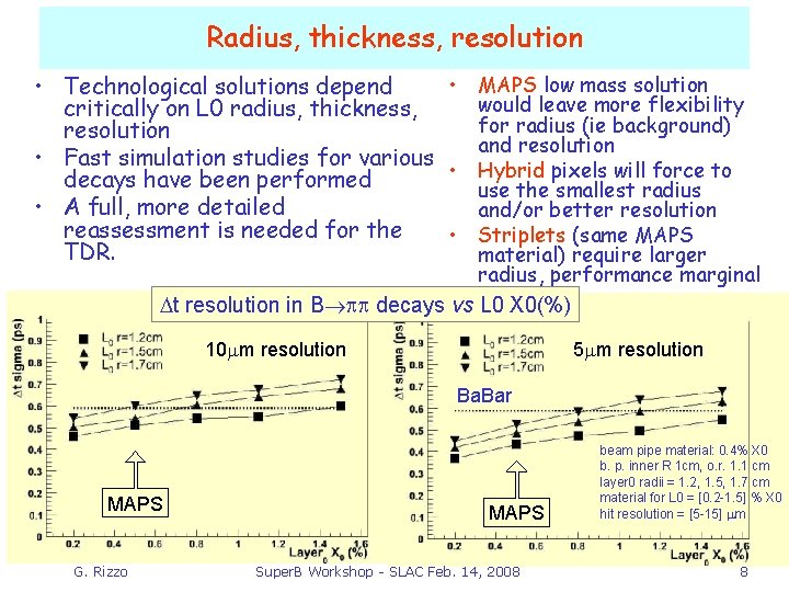
Radius, thickness, resolution • MAPS low mass solution • Technological solutions depend would leave more flexibility critically on L 0 radius, thickness, for radius (ie background) resolution and resolution • Fast simulation studies for various • Hybrid pixels will force to decays have been performed use the smallest radius • A full, more detailed and/or better resolution reassessment is needed for the • Striplets (same MAPS TDR. material) require larger radius, performance marginal Dt resolution in B pp decays vs L 0 X 0(%) 10 mm resolution 5 mm resolution Ba. Bar MAPS G. Rizzo MAPS Super. B Workshop - SLAC Feb. 14, 2008 beam pipe material: 0. 4% X 0 b. p. inner R 1 cm, o. r. 1. 1 cm layer 0 radii = 1. 2, 1. 5, 1. 7 cm material for L 0 = [0. 2 -1. 5] % X 0 hit resolution = [5 -15] mm 8

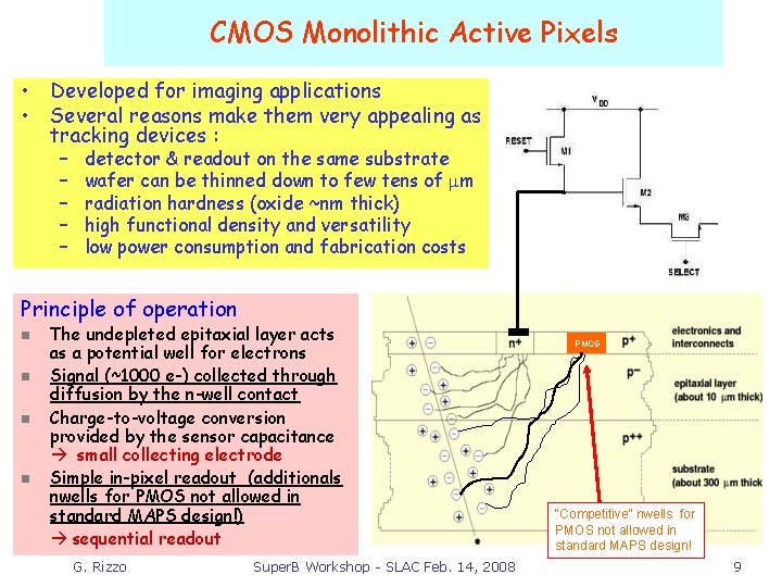
CMOS Monolithic Active Pixels • Developed for imaging applications • Several reasons make them very appealing as tracking devices : – – – detector & readout on the same substrate wafer can be thinned down to few tens of mm radiation hardness (oxide ~nm thick) high functional density and versatility low power consumption and fabrication costs Principle of operation n n The undepleted epitaxial layer acts as a potential well for electrons Signal (~1000 e-) collected through diffusion by the n-well contact Charge-to-voltage conversion provided by the sensor capacitance small collecting electrode Simple in-pixel readout (additionals nwells for PMOS not allowed in standard MAPS design!) sequential readout G. Rizzo Super. B Workshop - SLAC Feb. 14, 2008 PMOS “Competitive” nwells for PMOS not allowed in standard MAPS design! 9

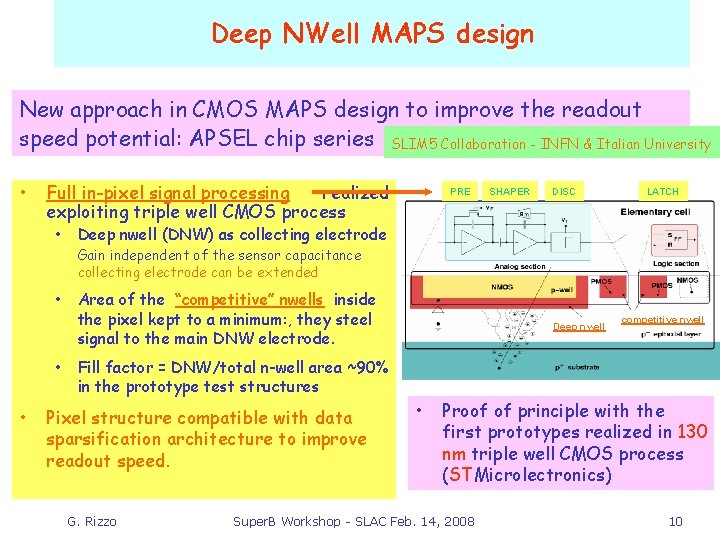
Deep NWell MAPS design New approach in CMOS MAPS design to improve the readout speed potential: APSEL chip series SLIM 5 Collaboration - INFN & Italian University • Full in-pixel signal processing realized exploiting triple well CMOS process PRE SHAPER DISC LATCH • Deep nwell (DNW) as collecting electrode Gain independent of the sensor capacitance collecting electrode can be extended • Area of the “competitive” nwells inside the pixel kept to a minimum: , they steel signal to the main DNW electrode. • Fill factor = DNW/total n-well area ~90% in the prototype test structures • Pixel structure compatible with data sparsification architecture to improve readout speed. G. Rizzo Deep nwell • competitive nwell Proof of principle with the first prototypes realized in 130 nm triple well CMOS process (STMicrolectronics) Super. B Workshop - SLAC Feb. 14, 2008 10

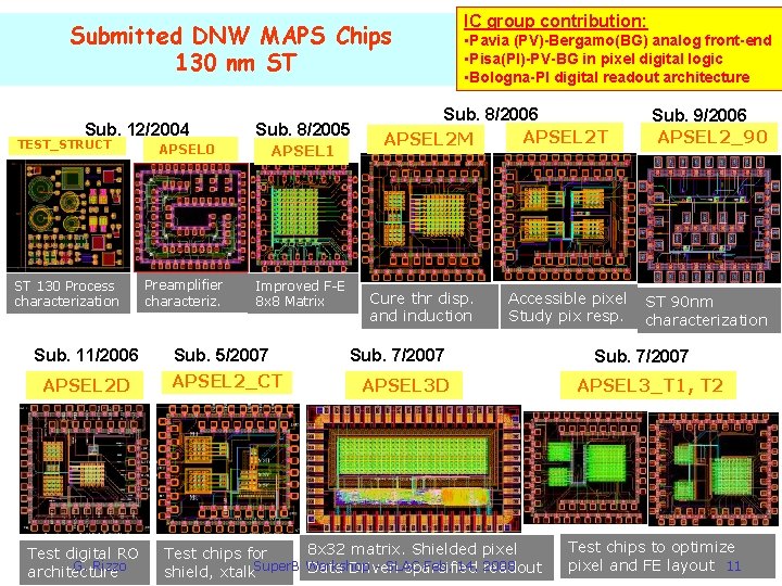
Submitted DNW MAPS Chips 130 nm ST Sub. 12/2004 Sub. 8/2005 TEST_STRUCT APSEL 0 APSEL 1 ST 130 Process characterization Preamplifier characteriz. Improved F-E 8 x 8 Matrix Sub. 11/2006 APSEL 2 D Test digital RO G. Rizzo architecture Sub. 5/2007 APSEL 2_CT IC group contribution: • Pavia (PV)-Bergamo(BG) analog front-end • Pisa(PI)-PV-BG in pixel digital logic • Bologna-PI digital readout architecture Sub. 8/2006 APSEL 2 T APSEL 2 M Cure thr disp. and induction Accessible pixel Study pix resp. Sub. 7/2007 APSEL 3 D 8 x 32 matrix. Shielded pixel Test chips for - SLAC Feb. 14, 2008 Data Driven sparsified readout shield, xtalk. Super. B Workshop Sub. 9/2006 APSEL 2_90 ST 90 nm characterization Sub. 7/2007 APSEL 3_T 1, T 2 Test chips to optimize pixel and FE layout 11

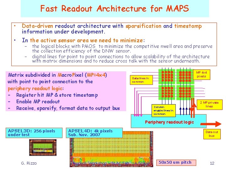
Fast Readout Architecture for MAPS • Data-driven readout architecture with sparsification and timestamp information under development. • In the active sensor area we need to minimize: – – the logical blocks with PMOS to minimize the competitive nwell area and preserve the collection efficiency of the DNW sensor. digital lines for point to point connections to allow scalability of the architecture with matrix dimensions and to reduce cross talk with the sensor underneath. Matrix subdivided in Macro. Pixel (MP=4 x 4) with point to point connection to the periphery readout logic: – Register hit MP & store timestamp – Enable MP readout – Receive, sparsify, format data to output bus MP 4 x 4 pixels Data lines in common Column enable lines in common 2 MP private lines Periphery readout logic APSEL 3 D: 256 pixels under test G. Rizzo APSEL 4 D: 4 k pixels Data out bus Sub. Nov. 2007 Super. B Workshop - SLAC Feb. 14, 2008 50 x 50 um pitch 12

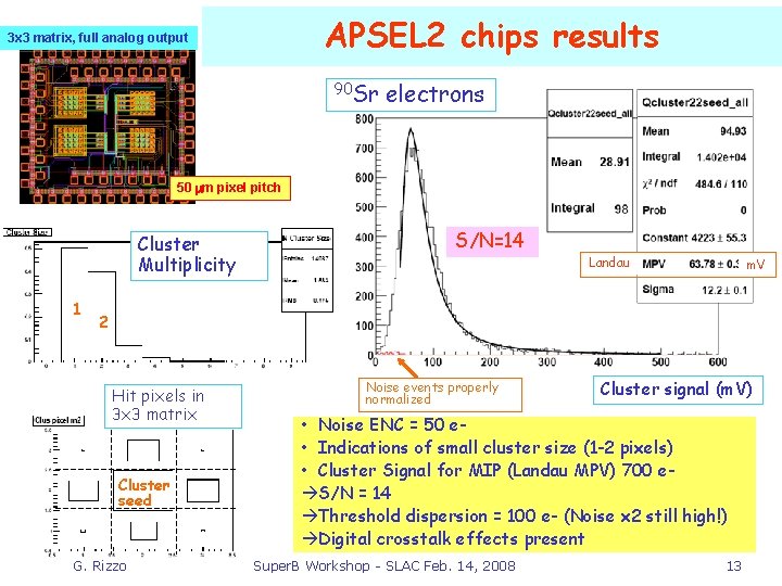
APSEL 2 chips results 3 x 3 matrix, full analog output 90 Sr electrons 50 mm pixel pitch Cluster Multiplicity 1 S/N=14 Landau m. V 2 Hit pixels in 3 x 3 matrix Cluster seed G. Rizzo Noise events properly normalized Cluster signal (m. V) • Noise ENC = 50 e • Indications of small cluster size (1 -2 pixels) • Cluster Signal for MIP (Landau MPV) 700 e S/N = 14 Threshold dispersion = 100 e- (Noise x 2 still high!) Digital crosstalk effects present Super. B Workshop - SLAC Feb. 14, 2008 13

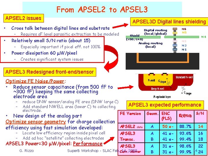
From APSEL 2 to APSEL 3 APSEL 2 issues • • • APSEL 3 D Digital lines shielding Cross talk between digital lines and substrate – Requires a. F level parasitic extraction to be modeled Relatively small S/N ratio (about 15) – Especially important if pixel eff. not 100% Digital routing (local/global) Shield (VDD/GND) Analog routing (local) Power dissipation 60 m. W/pixel – M 6 M 5 M 4 M 3 M 2 M 1 Creates significant system issues APSEL 3 Redesigned front-end/sensor Optimize FE Noise/Power: • Reduce sensor capacitance (from 500 f. F to ~300 f. F) keeping the same collecting electrode area – – reduce DNW sensor/analog FE area (DNW large C) Add standard NWELL area (lower C) to collecting electrode. • New design of the analog part Optimize sensor geometry for charge collection efficiency using fast simulation developed: – – Locate low efficiency region inside pixel cell Add ad hoc “satellite” collecting electrodes APSEL 3 Power=30 m. W/pixel: Performance G. Rizzo APSEL 3 expected performance FE Version APSEL 2 Geom. ENC (PLS) e(@5 s) S/N A 50 e- 88. 7% 14 APSEL 3 Transc. A B 41 e- 93. 6% 99. 4% 16 18 APSEL 3 A B 31 e- 98. 6% 22 99. 9% 14 24 data Super. B Workshop - SLAC Feb. Curr. 14, 2008 Mirror

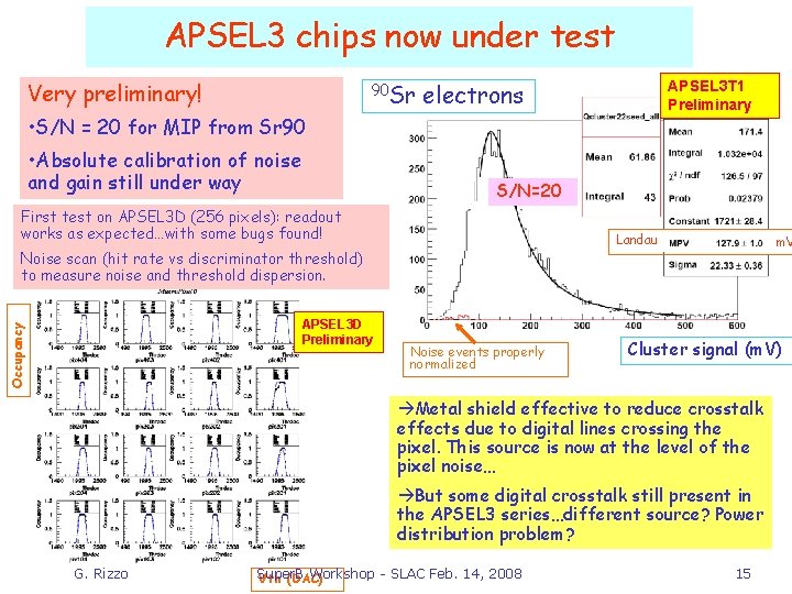
APSEL 3 chips now under test Very preliminary! 90 Sr electrons APSEL 3 T 1 Preliminary • S/N = 20 for MIP from Sr 90 • Absolute calibration of noise and gain still under way S/N=20 First test on APSEL 3 D (256 pixels): readout works as expected…with some bugs found! Landau Noise scan (hit rate vs discriminator threshold) to measure noise and threshold dispersion. Occupancy APSEL 3 D Preliminary Noise events properly normalized m. V Cluster signal (m. V) Metal shield effective to reduce crosstalk effects due to digital lines crossing the pixel. This source is now at the level of the pixel noise… But some digital crosstalk still present in the APSEL 3 series…different source? Power distribution problem? G. Rizzo Super. B Workshop - SLAC Feb. 14, 2008 Vth (DAC) 15

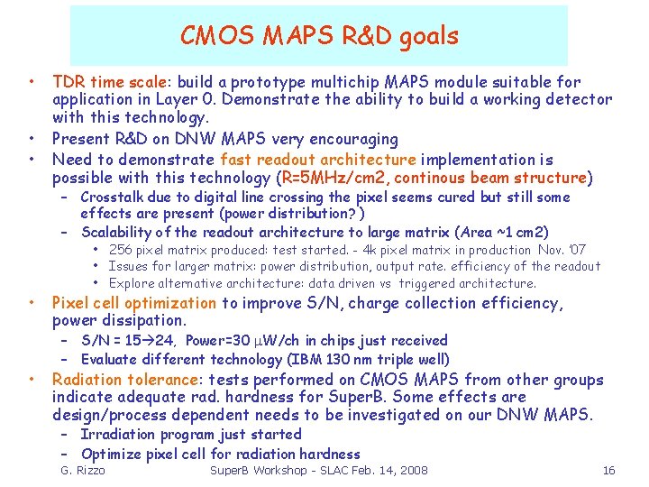
CMOS MAPS R&D goals • • • TDR time scale: build a prototype multichip MAPS module suitable for application in Layer 0. Demonstrate the ability to build a working detector with this technology. Present R&D on DNW MAPS very encouraging Need to demonstrate fast readout architecture implementation is possible with this technology (R=5 MHz/cm 2, continous beam structure) – Crosstalk due to digital line crossing the pixel seems cured but still some effects are present (power distribution? ) – Scalability of the readout architecture to large matrix (Area ~1 cm 2) • • • 256 pixel matrix produced: test started. - 4 k pixel matrix in production Nov. ’ 07 • Issues for larger matrix: power distribution, output rate. efficiency of the readout • Explore alternative architecture: data driven vs triggered architecture. Pixel cell optimization to improve S/N, charge collection efficiency, power dissipation. – S/N = 15 24, Power=30 m. W/ch in chips just received – Evaluate different technology (IBM 130 nm triple well) Radiation tolerance: tests performed on CMOS MAPS from other groups indicate adequate rad. hardness for Super. B. Some effects are design/process dependent needs to be investigated on our DNW MAPS. – Irradiation program just started – Optimize pixel cell for radiation hardness G. Rizzo Super. B Workshop - SLAC Feb. 14, 2008 16

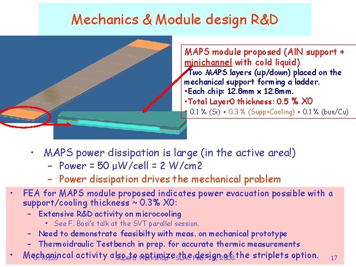
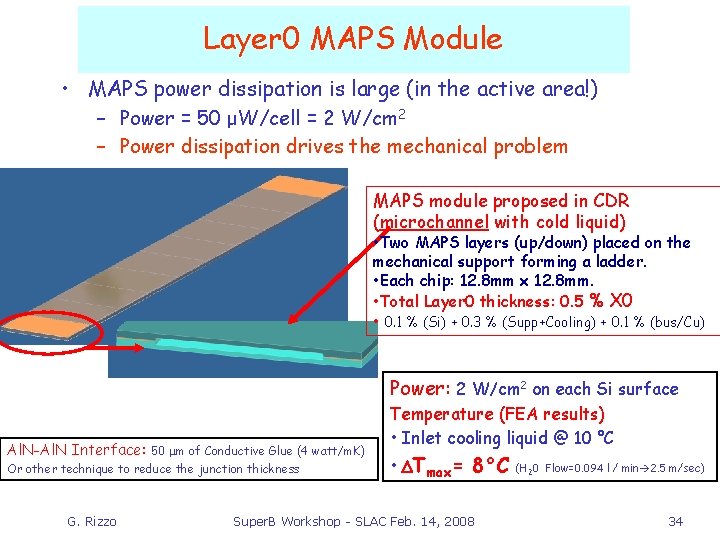
Mechanics & Module design R&D MAPS module proposed (Al. N support + minichannel with cold liquid) • Two MAPS layers (up/down) placed on the mechanical support forming a ladder. • Each chip: 12. 8 mm x 12. 8 mm. • Total Layer 0 thickness: 0. 5 % X 0 • 0. 1 % (Si) + 0. 3 % (Supp+Cooling) + 0. 1 % (bus/Cu) • MAPS power dissipation is large (in the active area!) – Power = 50 μW/cell = 2 W/cm 2 – Power dissipation drives the mechanical problem • FEA for MAPS module proposed indicates power evacuation possible with a support/cooling thickness ~ 0. 3% X 0: – Extensive R&D activity on microcooling • See F. Bosi’s talk at the SVT parallel session. • – Need to demonstrate feasibilty with meas. on mechanical prototype – Thermoidraulic Testbench in prep. for accurate thermic measurements Mechanincal activity also to Workshop optimize the Feb. design of the striplets option. G. Rizzo Super. B - SLAC 14, 2008 17

Explore more advanced technological solutions • Improvements w. r. t explored Layer 0 solutions could be achieved with: – Vertical Integration of thin chips: • high resistivity pixel sensor + CMOS readout chip in less than 100 um. – Integration of microcooling techniques on Si chips themselves • Hopefully start R&D by the end of 2008 (PRIN Project submitted, pending approval …) • These technologies might not be ready when the Super. B construction starts but could be mature for an upgrade of Layer 0 (we need to design an interaction region with easier access & replacement). G. Rizzo Super. B Workshop - SLAC Feb. 14, 2008 18

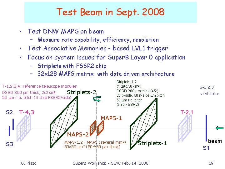
Test Beam in Sept. 2008 • Test DNW MAPS on beam – Measure rate capability, efficiency, resolution • Test Associative Memories - based LVL 1 trigger • Focus on system issues for Super. B Layer 0 application – Striplets with FSSR 2 chip – 32 x 128 MAPS matrix with data driven architecture T-1, 2, 3, 4 : reference telescope modules DSSD 300 mm thick, 2 x 2 cm 2 Striplets-2 50 mm r. o. pitch (3 chip FSSR 2/side) S 2 T-4, 3 Striplets-1, 2: (1. 29 x 7. 0 cm 2 ) DSSD 200 mm thick (45 o) 25 p-side, 50 n-side mm pitch 50 mm r. o. pitch (chip FSSR 2) S-1, 2, 3 scintillator T-2, 1 MAPS-2 MAPS-1, 2 : MAPS (several mm 2) 50 x 50 mm 2 (50 80 mm-thick) S 3 G. Rizzo Striplets-1 Super. B Workshop - SLAC Feb. 14, 2008 beam S 1 19

Conclusions • We have an SVT detector concept based on Babar with modifications required to operate at a L=1036 cm-2 s-1 and with the reduced Super. B boost: Ba. Bar SVT + Layer 0 • Still, a significant amount of work is needed to turn this concept into a full detector design and write a Technical Design Report: – Strong ongoing R&D on technology development for Layer 0 (MAPS, low mass cooling…) – Physics studies to optimize overall detector geometry – Background studies to optimize detector space-time granularity and verify radiation levels – Detector physics-engineering studies to produce a sound subsystem design – Activities in some areas not yet covered but need to start soon • More details on where we stand in this process and plans for future developments will be presented in the SVT parallel session (Friday morning). G. Rizzo Super. B Workshop - SLAC Feb. 14, 2008 20

backup G. Rizzo Super. B Workshop - SLAC Feb. 14, 2008 21

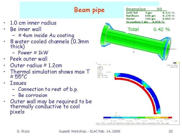
Beam pipe • 1. 0 cm inner radius • Be inner wall – ≈ 4 um inside Au coating • 8 water cooled channels (0. 3 mm thick) – Power ≈ 1 k. W • Peek outer wall • Outer radius ≈ 1. 2 cm • Thermal simulation shows max T ≈ 55°C • Issues – Connection to rest of b. p. – Be corrosion • Outer wall may be required to be thermally conductive to cool pixels G. Rizzo Super. B Workshop - SLAC Feb. 14, 2008 Beampipe Gold foil Berillium Water Ni coating 7 Total X 0 4 mm 600 mm 300 mm mm 0. 050 0. 121 % 0. 170 % 0. 083 % % 0. 42 % 22

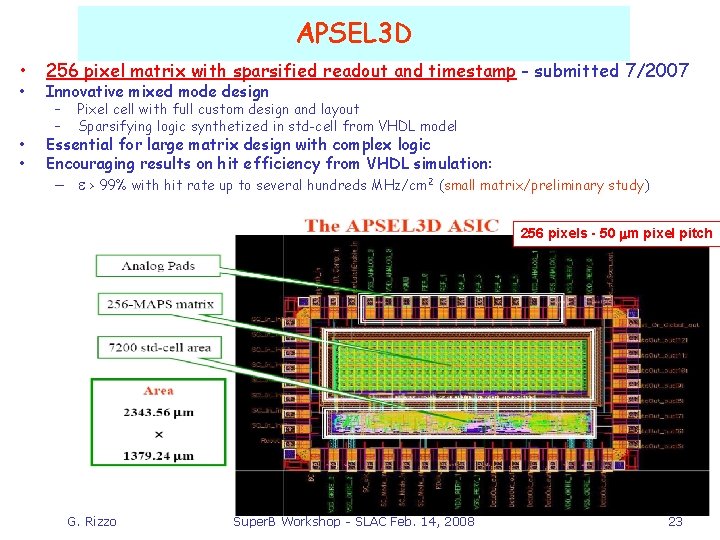
APSEL 3 D • • 256 pixel matrix with sparsified readout and timestamp - submitted 7/2007 Innovative mixed mode design – – Pixel cell with full custom design and layout Sparsifying logic synthetized in std-cell from VHDL model Essential for large matrix design with complex logic Encouraging results on hit efficiency from VHDL simulation: – e > 99% with hit rate up to several hundreds MHz/cm 2 (small matrix/preliminary study) 256 pixels - 50 mm pixel pitch G. Rizzo Super. B Workshop - SLAC Feb. 14, 2008 23

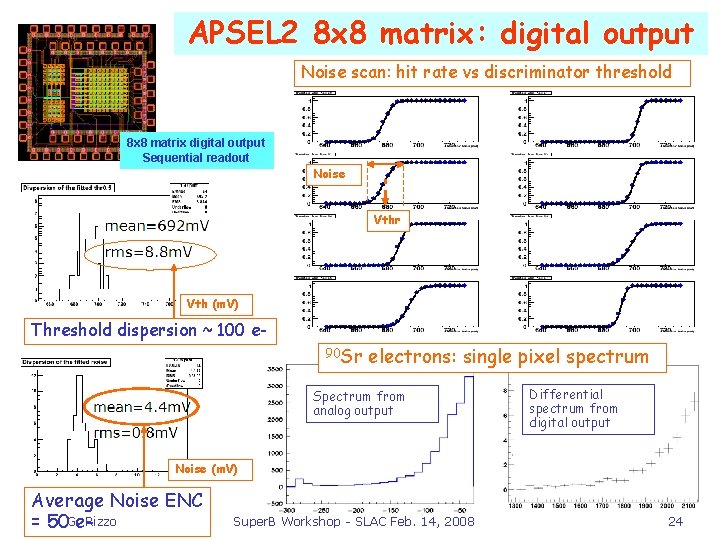
APSEL 2 8 x 8 matrix: digital output Noise scan: hit rate vs discriminator threshold 8 x 8 matrix digital output Sequential readout Noise Vthr Vth (m. V) Threshold dispersion ~ 100 e 90 Sr electrons: single pixel spectrum Spectrum from analog output Differential spectrum from digital output Noise (m. V) Average Noise ENC = 50 G. e-Rizzo Super. B Workshop - SLAC Feb. 14, 2008 24

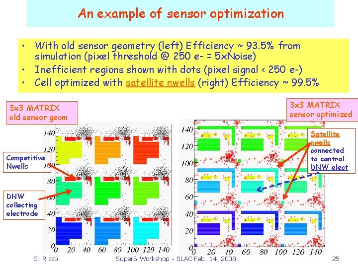
An example of sensor optimization • With old sensor geometry (left) Efficiency ~ 93. 5% from simulation (pixel threshold @ 250 e- = 5 x. Noise) • Inefficient regions shown with dots (pixel signal < 250 e-) • Cell optimized with satellite nwells (right) Efficiency ~ 99. 5% 3 x 3 MATRIX sensor optimized 3 x 3 MATRIX old sensor geom Satellite nwells connected to central DNW elect Competitive Nwells DNW collecting electrode G. Rizzo Super. B Workshop - SLAC Feb. 14, 2008 25

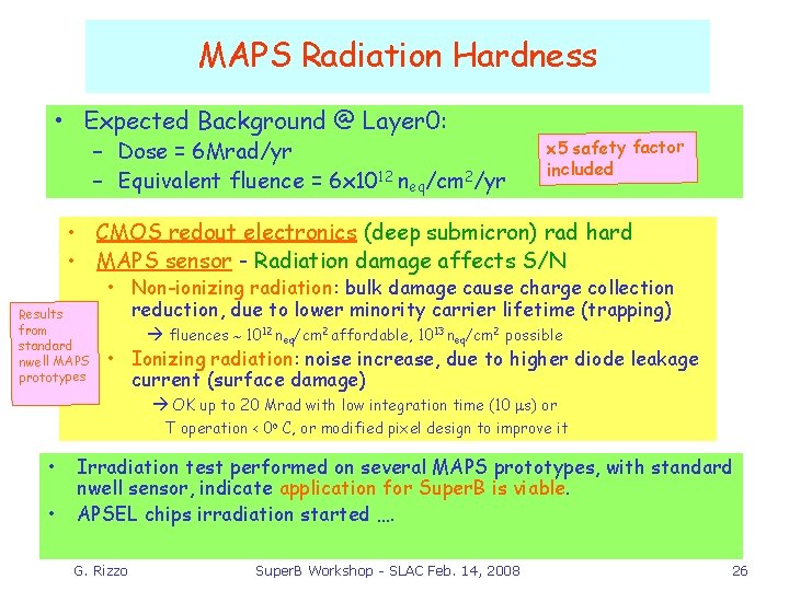
MAPS Radiation Hardness • Expected Background @ Layer 0: – Dose = 6 Mrad/yr – Equivalent fluence = 6 x 10¹² neq/cm 2/yr x 5 safety factor included • CMOS redout electronics (deep submicron) rad hard • MAPS sensor - Radiation damage affects S/N Results from standard nwell MAPS prototypes • Non-ionizing radiation: bulk damage cause charge collection reduction, due to lower minority carrier lifetime (trapping) fluences ~ 1012 neq/cm 2 affordable, 1013 neq/cm 2 possible • Ionizing radiation: noise increase, due to higher diode leakage current (surface damage) OK up to 20 Mrad with low integration time (10 ms) or T operation < 0 o C, or modified pixel design to improve it • • Irradiation test performed on several MAPS prototypes, with standard nwell sensor, indicate application for Super. B is viable. APSEL chips irradiation started …. G. Rizzo Super. B Workshop - SLAC Feb. 14, 2008 26

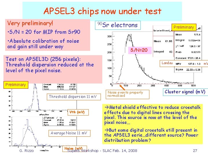
APSEL 3 chips now under test Very preliminary! • S/N = 20 for MIP from Sr 90 • Absolute calibration of noise and gain still under way 90 Sr electrons Preliminary S/N=20 Test on APSEL 3 D (256 pixels): Threshold dispersion reduced at the level of the pixel noise. Landau m. V Preliminary Threshold dispersion 11 m. V Vth (m. V) Average Noise 11 m. V G. Rizzo Noise events properly normalized Cluster signal (m. V) Metal shield effective to reduce crosstalk effects due to digital lines crossing the pixel. This source is now at the level of the pixel noise… But some digital crosstalk still present in the APSEL 3 serie…different source? Power distribution problem? Noise (m. V) Super. B Workshop - SLAC Feb. 14, 2008 27

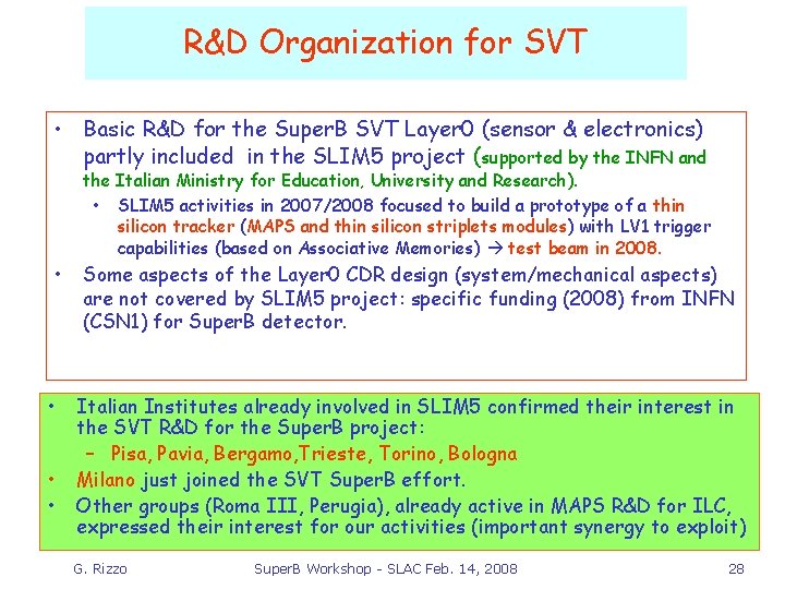
R&D Organization for SVT • Basic R&D for the Super. B SVT Layer 0 (sensor & electronics) partly included in the SLIM 5 project (supported by the INFN and the Italian Ministry for Education, University and Research). • SLIM 5 activities in 2007/2008 focused to build a prototype of a thin silicon tracker (MAPS and thin silicon striplets modules) with LV 1 trigger capabilities (based on Associative Memories) test beam in 2008. • • Some aspects of the Layer 0 CDR design (system/mechanical aspects) are not covered by SLIM 5 project: specific funding (2008) from INFN (CSN 1) for Super. B detector. Italian Institutes already involved in SLIM 5 confirmed their interest in the SVT R&D for the Super. B project: – Pisa, Pavia, Bergamo, Trieste, Torino, Bologna Milano just joined the SVT Super. B effort. Other groups (Roma III, Perugia), already active in MAPS R&D for ILC, expressed their interest for our activities (important synergy to exploit) G. Rizzo Super. B Workshop - SLAC Feb. 14, 2008 28

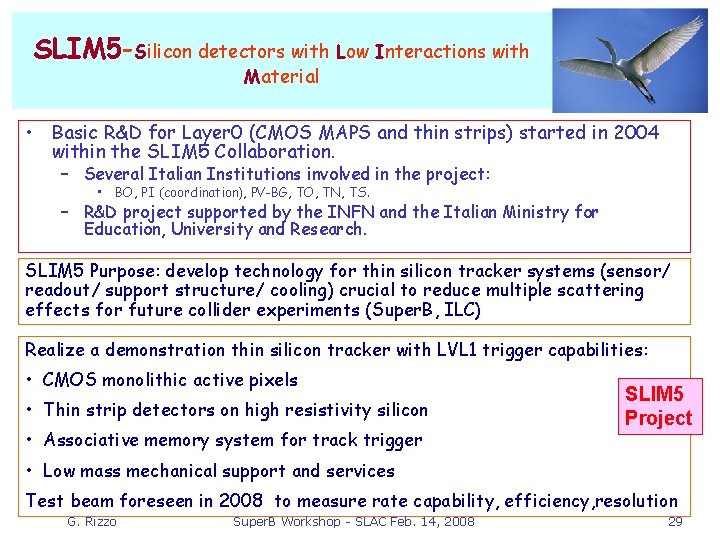
SLIM 5 -Silicon detectors with Low Interactions with Material • Basic R&D for Layer 0 (CMOS MAPS and thin strips) started in 2004 within the SLIM 5 Collaboration. – Several Italian Institutions involved in the project: • BO, PI (coordination), PV-BG, TO, TN, TS. – R&D project supported by the INFN and the Italian Ministry for Education, University and Research. SLIM 5 Purpose: develop technology for thin silicon tracker systems (sensor/ readout/ support structure/ cooling) crucial to reduce multiple scattering effects for future collider experiments (Super. B, ILC) Realize a demonstration thin silicon tracker with LVL 1 trigger capabilities: • CMOS monolithic active pixels • Thin strip detectors on high resistivity silicon • Associative memory system for track trigger SLIM 5 Project • Low mass mechanical support and services Test beam foreseen in 2008 to measure rate capability, efficiency, resolution G. Rizzo Super. B Workshop - SLAC Feb. 14, 2008 29

SLIM 5 -Silicon detectors with Low Interactions with Material G. Batignani 1, 2, S. Bettarini 1, 2, F. Bosi 1, 2, G. Calderini 1, 2, R. Cenci 1, 2, M. Dell’Orso 1, 2, F. Forti 1, 2, P. Giannetti 1, 2 , M. A. Giorgi 1, 2, A. Lusiani 2, 3, G. Marchiori 1, 2, F. Morsani 2, N. Neri 2, E. Paoloni 1, 2, G. Rizzo 1, 2 , J. Walsh 2 C. Andreoli 4, 5, E. Pozzati 4, 5, L. Ratti 4, 5, V. Speziali 4, 5, M. Manghisoni 5, 6, V. Re 5, 6, G. Traversi 5, 6, L. Gaioni 4, 5 L. Bosisio 7, G. Giacomini 7, L. Lanceri 7, I. Rachevskaia 7, L. Vitale 7, M. Bruschi 8, B. Giacobbe 8, A. Gabrielli 8, N. Semprini 8, R. Spighi 8, M. Villa 8, A. Zoccoli 8, D. Gamba 9, G. Giraudo 9, P. Mereu 9, G. F. Dalla Betta 10 , G. Soncini 10 , G. Fontana 10 , L. Pancheri 10 , G. Verzellesi 11 1 Università degli Studi di Pisa, 2 INFN Pisa, 3 Scuola Normale Superiore di Pisa, 4 Università degli Studi di Pavia, 5 INFN Pavia, 6 Università 7 INFN 8 INFN Trieste and Università degli Studi di Trieste Bologna and Università degli Studi di Bologna 9 INFN Torino and Università degli Studi di Torino 10 Università 11 Università G. Rizzo degli Studi di Bergamo, degli Studi di Trento and INFN Padova degli Studi di Modena e Reggio Emilia and INFN Padova Super. B Workshop - SLAC Feb. 14, 2008 30

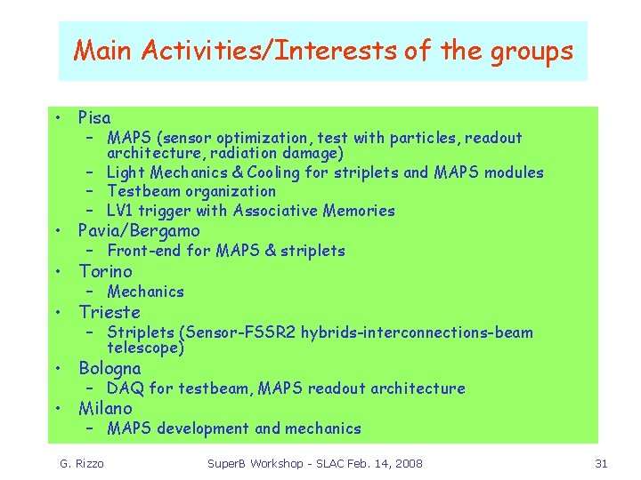
Main Activities/Interests of the groups • Pisa – MAPS (sensor optimization, test with particles, readout architecture, radiation damage) – Light Mechanics & Cooling for striplets and MAPS modules – Testbeam organization – LV 1 trigger with Associative Memories • Pavia/Bergamo – Front-end for MAPS & striplets • Torino – Mechanics • Trieste – Striplets (Sensor-FSSR 2 hybrids-interconnections-beam telescope) • Bologna – DAQ for testbeam, MAPS readout architecture • Milano – MAPS development and mechanics G. Rizzo Super. B Workshop - SLAC Feb. 14, 2008 31

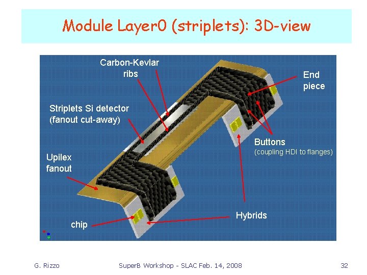
Module Layer 0 (striplets): 3 D-view Carbon-Kevlar ribs End piece Striplets Si detector (fanout cut-away) Buttons (coupling HDI to flanges) Upilex fanout chip G. Rizzo Hybrids Super. B Workshop - SLAC Feb. 14, 2008 32

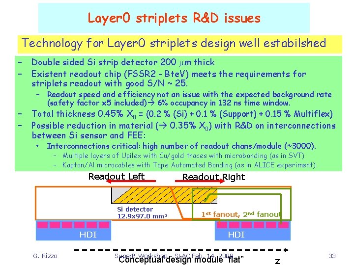
Layer 0 striplets R&D issues Technology for Layer 0 striplets design well estabilshed – – Double sided Si strip detector 200 mm thick Existent readout chip (FSSR 2 - Bte. V) meets the requirements for striplets readout with good S/N ~ 25. – Readout speed and efficiency not an issue with the expected background rate (safety factor x 5 included) 6% occupancy in 132 ns time window. Total thickness 0. 45% X 0 = (0. 2 % (Si) + 0. 1 % (Support) + 0. 15 % Multiflex) Possible reduction in material ( 0. 35% X 0) with R&D on interconnections between Si sensor and FEE: • Interconnections critical: high number of readout chans/module (~3000). – Multiple layers of Upilex with Cu/gold traces with microbonding (as in SVT) – Kapton/Al microcables with Tape Automated Bonding (as in ALICE experiment) Readout Left Si detector 12. 9 x 97. 0 mm 2 HDI G. Rizzo Readout Right 1 st fanout, 2 nd fanout HDI Super. B Workshop - SLAC Feb. 14, 2008 Conceptual design module “flat” z 33

Layer 0 MAPS Module • MAPS power dissipation is large (in the active area!) – Power = 50 μW/cell = 2 W/cm 2 – Power dissipation drives the mechanical problem MAPS module proposed in CDR (microchannel with cold liquid) • Two MAPS layers (up/down) placed on the mechanical support forming a ladder. • Each chip: 12. 8 mm x 12. 8 mm. • Total Layer 0 thickness: 0. 5 % X 0 • 0. 1 % (Si) + 0. 3 % (Supp+Cooling) + 0. 1 % (bus/Cu) Power: 2 W/cm 2 on each Si surface Al. N-Al. N Interface: 50 mm of Conductive Glue (4 watt/m. K) Or other technique to reduce the junction thickness G. Rizzo Temperature (FEA results) • Inlet cooling liquid @ 10 °C • DTmax= 8°C Super. B Workshop - SLAC Feb. 14, 2008 (H 20 Flow=0. 094 l / min 2. 5 m/sec) 34

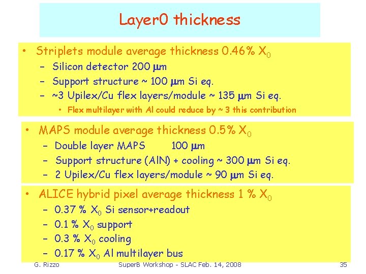
Layer 0 thickness • Striplets module average thickness 0. 46% X 0 – Silicon detector 200 mm – Support structure ~ 100 mm Si eq. – ~3 Upilex/Cu flex layers/module ~ 135 mm Si eq. • Flex multilayer with Al could reduce by ~ 3 this contribution • MAPS module average thickness 0. 5% X 0 – Double layer MAPS 100 mm – Support structure (Al. N) + cooling ~ 300 mm Si eq. – 2 Upilex/Cu flex layers/module ~ 90 mm Si eq. • ALICE hybrid pixel average thickness 1 % X 0 – – 0. 37 % X 0 Si sensor+readout 0. 1 % X 0 support 0. 3 % X 0 cooling 0. 17 % X 0 Al multilayer bus G. Rizzo Super. B Workshop - SLAC Feb. 14, 2008 35