ECE 313 Computer Organization Lecture 11 Processor Implementation
![Register Transfers for the MIPS Subset } Instruction Fetch Instruction <- MEM[PC] } Instruction Register Transfers for the MIPS Subset } Instruction Fetch Instruction <- MEM[PC] } Instruction](https://slidetodoc.com/presentation_image_h2/f32e0b3e2c8098475ca06d59e2c3f5ba/image-13.jpg)
![Datapath for Instruction Fetch Instruction <- MEM[PC] PC <- PC + 4 ECE 313 Datapath for Instruction Fetch Instruction <- MEM[PC] PC <- PC + 4 ECE 313](https://slidetodoc.com/presentation_image_h2/f32e0b3e2c8098475ca06d59e2c3f5ba/image-27.jpg)
![Datapath for R-Type Instructions add rd, rs, rt R[rd] <- R[rs] + R[rt]; ECE Datapath for R-Type Instructions add rd, rs, rt R[rd] <- R[rs] + R[rt]; ECE](https://slidetodoc.com/presentation_image_h2/f32e0b3e2c8098475ca06d59e2c3f5ba/image-28.jpg)
![Datapath for Load/Store Instructions lw rt, offset(rs) R[rt] <- MEM[R[rs] + s_extend(offset)]; ECE 313 Datapath for Load/Store Instructions lw rt, offset(rs) R[rt] <- MEM[R[rs] + s_extend(offset)]; ECE 313](https://slidetodoc.com/presentation_image_h2/f32e0b3e2c8098475ca06d59e2c3f5ba/image-29.jpg)
![Datapath for Load/Store Instructions sw rt, offset(rs) MEM[R[rs] + sign_extend(offset)] <- R[rt] ECE 313 Datapath for Load/Store Instructions sw rt, offset(rs) MEM[R[rs] + sign_extend(offset)] <- R[rt] ECE 313](https://slidetodoc.com/presentation_image_h2/f32e0b3e2c8098475ca06d59e2c3f5ba/image-30.jpg)
![Datapath for Branch Instructions beq rs, rt, offset if (R[rs] == R[rt]) then PC Datapath for Branch Instructions beq rs, rt, offset if (R[rs] == R[rt]) then PC](https://slidetodoc.com/presentation_image_h2/f32e0b3e2c8098475ca06d59e2c3f5ba/image-31.jpg)
- Slides: 71

ECE 313 - Computer Organization Lecture 11 - Processor Implementation: Overview, Single-Cycle Design Fall 2004 Reading: 5. 1 -5. 4 Homework Due 10/27: 4. 1, 4. 2, 4. 3, 4. 6, 4. 19 - 4. 22 Prof. John Nestor ECE Department Lafayette College Easton, Pennsylvania 18042 nestorj@lafayette. edu Portions of these slides are derived from: Textbook figures © 1998 Morgan Kaufmann Publishers all rights reserved Tod Amon's COD 2 e Slides © 1998 Morgan Kaufmann Publishers all rights reserved Dave Patterson’s CS 152 Slides - Fall 1997 © UCB Rob Rutenbar’s 18 -347 Slides - Fall 1999 CMU ECE 313 Fall 2004 Lecture 11 - Processor Design other sources as noted 1

Roadmap for the Term: Major Topics } } } } Computer Systems Overview Technology Trends Performance Instruction Sets (and Software) Logic and Arithmetic Processor Implementation Memory Systems Input/Output ECE 313 Fall 2004 Lecture 11 - Processor Design 2

Outline - Processor Implementation } Overview } } Review of Processor Operation Steps in Processor Design Implementation Styles The “MIPS Lite” Instruction Subset } Single-Cycle Implementation } Multi-Cycle Implementation } Pipelined Implementation ECE 313 Fall 2004 Lecture 11 - Processor Design 3

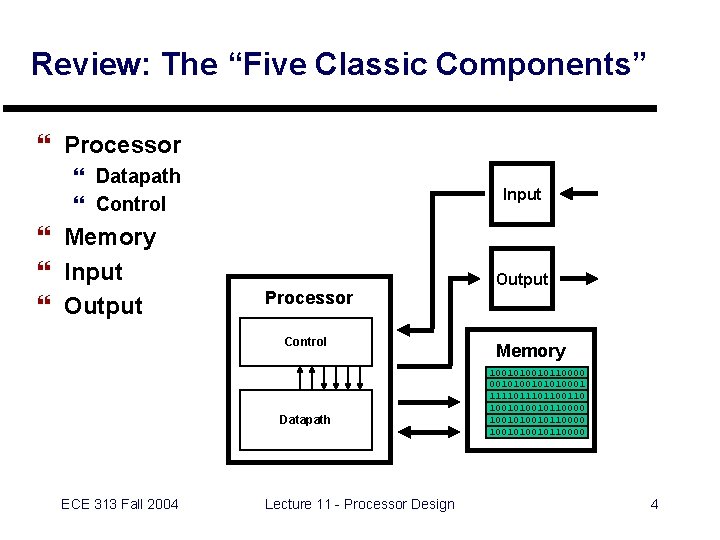
Review: The “Five Classic Components” } Processor } Datapath } Control } Memory } Input } Output Input Output Processor Control Datapath ECE 313 Fall 2004 Lecture 11 - Processor Design Memory 10010110000 00101010001 111101100110 1001010010110000 4

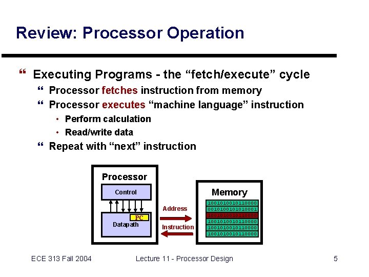
Review: Processor Operation } Executing Programs - the “fetch/execute” cycle } Processor fetches instruction from memory } Processor executes “machine language” instruction • Perform calculation • Read/write data } Repeat with “next” instruction Processor Memory Control Address PC Datapath ECE 313 Fall 2004 Instruction 10010110000 00101010001 10010110000 111101100110 1001010010110000 Lecture 11 - Processor Design 5

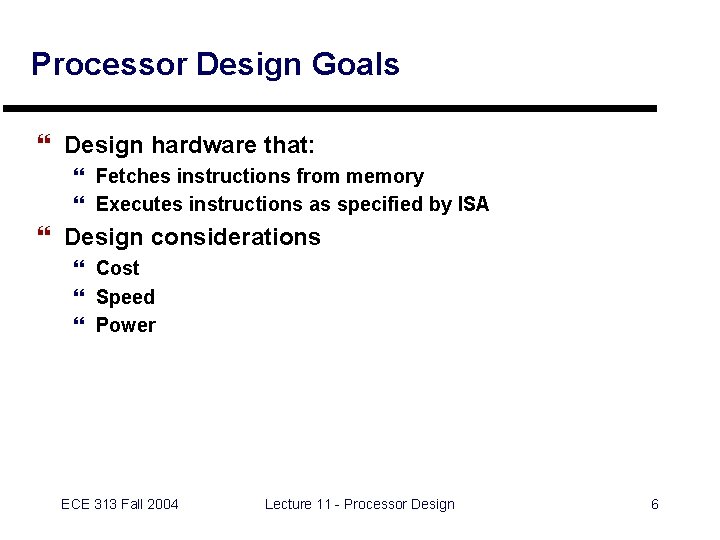
Processor Design Goals } Design hardware that: } Fetches instructions from memory } Executes instructions as specified by ISA } Design considerations } Cost } Speed } Power ECE 313 Fall 2004 Lecture 11 - Processor Design 6

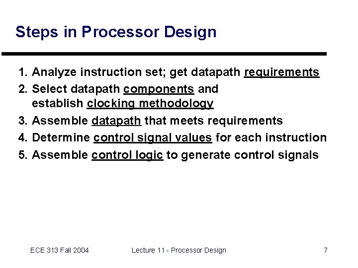
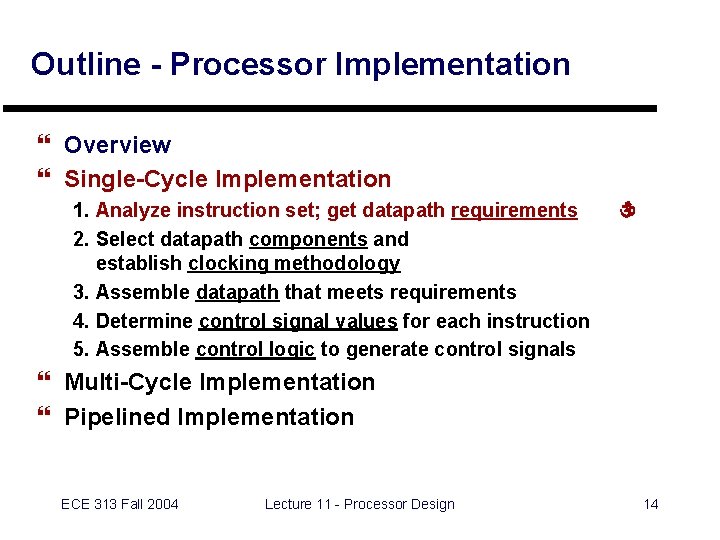
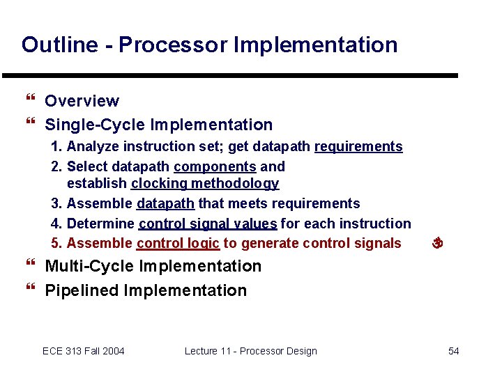
Steps in Processor Design 1. Analyze instruction set; get datapath requirements 2. Select datapath components and establish clocking methodology 3. Assemble datapath that meets requirements 4. Determine control signal values for each instruction 5. Assemble control logic to generate control signals ECE 313 Fall 2004 Lecture 11 - Processor Design 7

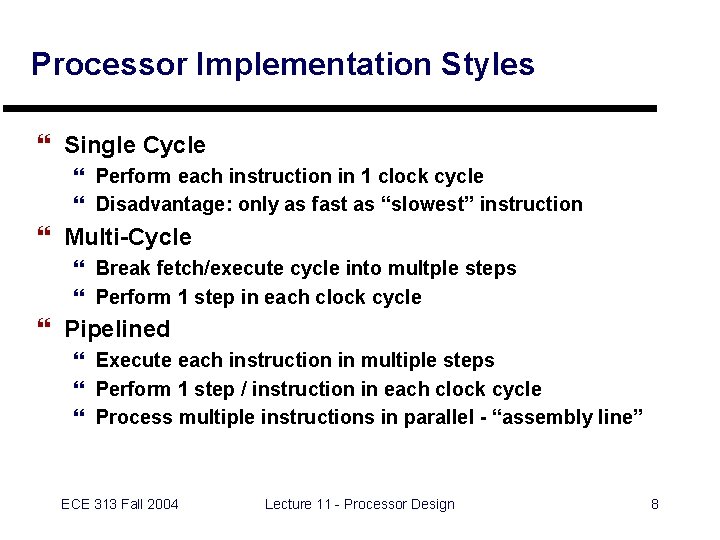
Processor Implementation Styles } Single Cycle } Perform each instruction in 1 clock cycle } Disadvantage: only as fast as “slowest” instruction } Multi-Cycle } Break fetch/execute cycle into multple steps } Perform 1 step in each clock cycle } Pipelined } Execute each instruction in multiple steps } Perform 1 step / instruction in each clock cycle } Process multiple instructions in parallel - “assembly line” ECE 313 Fall 2004 Lecture 11 - Processor Design 8

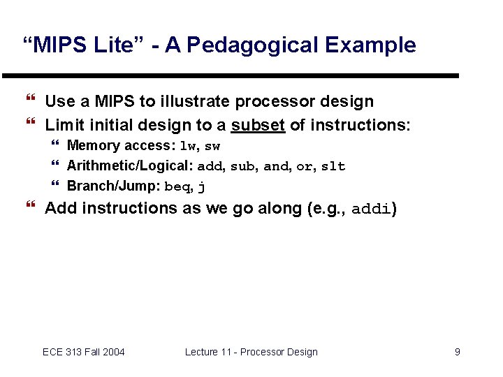
“MIPS Lite” - A Pedagogical Example } Use a MIPS to illustrate processor design } Limit initial design to a subset of instructions: } Memory access: lw, sw } Arithmetic/Logical: add, sub, and, or, slt } Branch/Jump: beq, j } Add instructions as we go along (e. g. , addi) ECE 313 Fall 2004 Lecture 11 - Processor Design 9

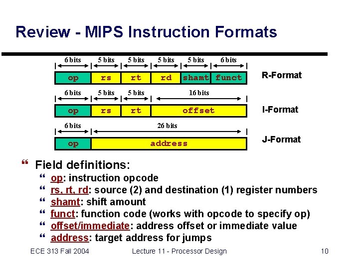
Review - MIPS Instruction Formats 6 bits 5 bits op rs rt rd 6 bits 5 bits 16 bits op rs rt offset 6 bits shamt funct 6 bits 26 bits op address R-Format I-Format J-Format } Field definitions: } } } op: instruction opcode rs, rt, rd: source (2) and destination (1) register numbers shamt: shift amount funct: function code (works with opcode to specify op) offset/immediate: address offset or immediate value address: target address for jumps ECE 313 Fall 2004 Lecture 11 - Processor Design 10

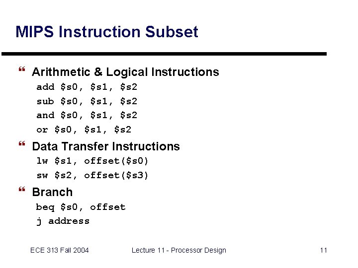
MIPS Instruction Subset } Arithmetic & Logical Instructions add $s 0, $s 1, $s 2 sub $s 0, $s 1, $s 2 and $s 0, $s 1, $s 2 or $s 0, $s 1, $s 2 } Data Transfer Instructions lw $s 1, offset($s 0) sw $s 2, offset($s 3) } Branch beq $s 0, offset j address ECE 313 Fall 2004 Lecture 11 - Processor Design 11

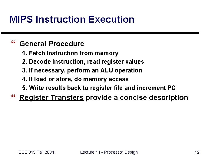
MIPS Instruction Execution } General Procedure 1. Fetch Instruction from memory 2. Decode Instruction, read register values 3. If necessary, perform an ALU operation 4. If load or store, do memory access 5. Write results back to register file and increment PC } Register Transfers provide a concise description ECE 313 Fall 2004 Lecture 11 - Processor Design 12
![Register Transfers for the MIPS Subset Instruction Fetch Instruction MEMPC Instruction Register Transfers for the MIPS Subset } Instruction Fetch Instruction <- MEM[PC] } Instruction](https://slidetodoc.com/presentation_image_h2/f32e0b3e2c8098475ca06d59e2c3f5ba/image-13.jpg)
Register Transfers for the MIPS Subset } Instruction Fetch Instruction <- MEM[PC] } Instruction Execution Instr. Register Transfers add sub and or lw sw beq R[rd] <- R[rs] + R[rt]; PC <- PC + 4 R[rd] <- R[rs] - R[rt]; PC <- PC + 4 R[rd] <- R[rs] & R[rt]; PC <- PC + 4 R[rd] <- R[rs] | R[rt]; PC <- PC + 4 R[rt] <- MEM[R[rs] + s_extend(offset)]; PC<- PC + 4 MEM[R[rs] + sign_extend(offset)] <- R[rt]; PC <- PC + 4 if (R[rs] == R[rt]) then PC <- PC+4 + s_extend(offset<<2) j else PC <- PC + 4 PC <- upper(PC)@(address << 2) ECE 313 Fall 2004 Lecture 11 - Processor Design 13

Outline - Processor Implementation } Overview } Single-Cycle Implementation 1. Analyze instruction set; get datapath requirements 2. Select datapath components and establish clocking methodology 3. Assemble datapath that meets requirements 4. Determine control signal values for each instruction 5. Assemble control logic to generate control signals } Multi-Cycle Implementation } Pipelined Implementation ECE 313 Fall 2004 Lecture 11 - Processor Design 14

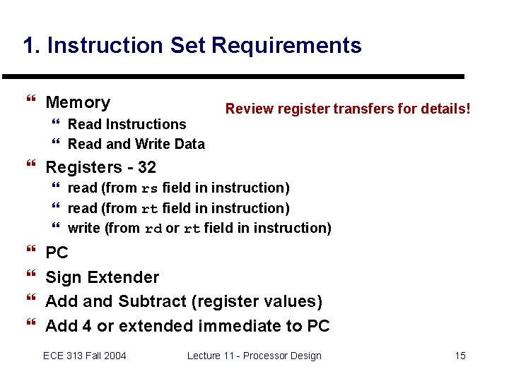
1. Instruction Set Requirements } Memory } Read Instructions } Read and Write Data Review register transfers for details! } Registers - 32 } read (from rs field in instruction) } read (from rt field in instruction) } write (from rd or rt field in instruction) } } PC Sign Extender Add and Subtract (register values) Add 4 or extended immediate to PC ECE 313 Fall 2004 Lecture 11 - Processor Design 15

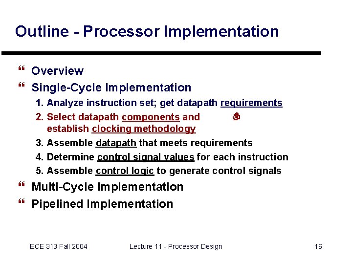
Outline - Processor Implementation } Overview } Single-Cycle Implementation 1. Analyze instruction set; get datapath requirements 2. Select datapath components and establish clocking methodology 3. Assemble datapath that meets requirements 4. Determine control signal values for each instruction 5. Assemble control logic to generate control signals } Multi-Cycle Implementation } Pipelined Implementation ECE 313 Fall 2004 Lecture 11 - Processor Design 16

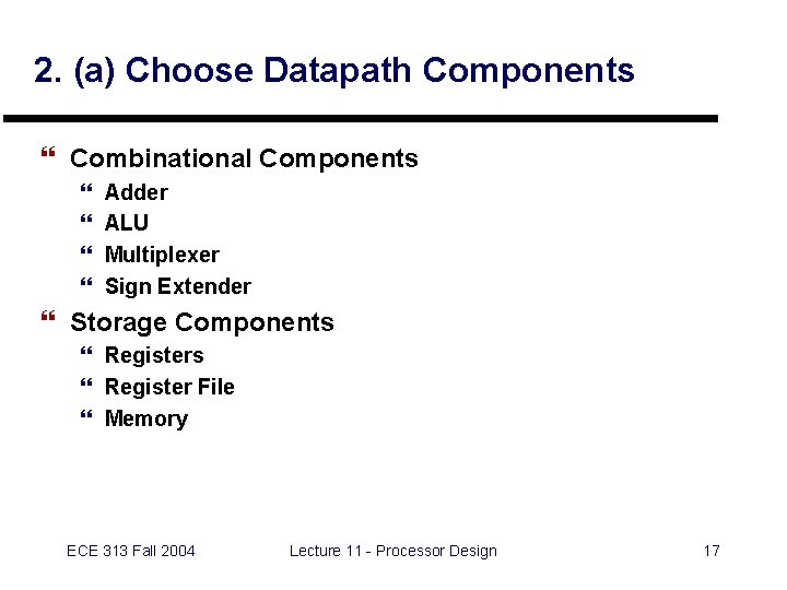
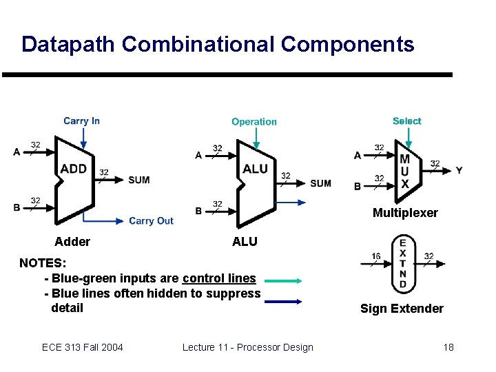
2. (a) Choose Datapath Components } Combinational Components } } Adder ALU Multiplexer Sign Extender } Storage Components } Register File } Memory ECE 313 Fall 2004 Lecture 11 - Processor Design 17

Datapath Combinational Components Multiplexer Adder ALU NOTES: - Blue-green inputs are control lines - Blue lines often hidden to suppress detail ECE 313 Fall 2004 Lecture 11 - Processor Design Sign Extender 18

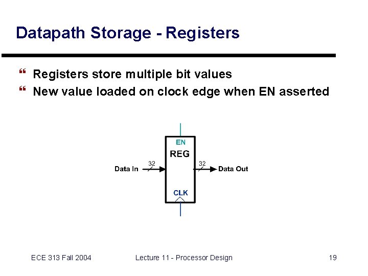
Datapath Storage - Registers } Registers store multiple bit values } New value loaded on clock edge when EN asserted ECE 313 Fall 2004 Lecture 11 - Processor Design 19

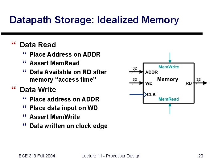
Datapath Storage: Idealized Memory } Data Read } Place Address on ADDR } Assert Mem. Read } Data Available on RD after memory “access time” } Data Write } } Place address on ADDR Place data input on WD Assert Mem. Write Data written on clock edge ECE 313 Fall 2004 Lecture 11 - Processor Design 20

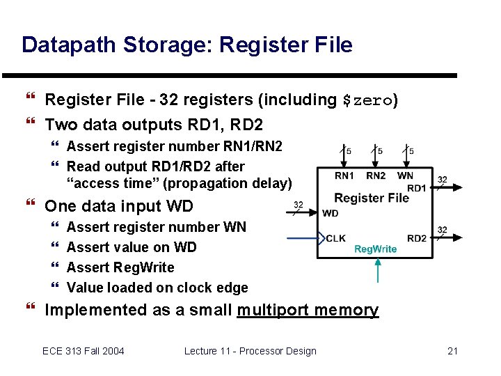
Datapath Storage: Register File } Register File - 32 registers (including $zero) } Two data outputs RD 1, RD 2 } Assert register number RN 1/RN 2 } Read output RD 1/RD 2 after “access time” (propagation delay) } One data input WD } } Assert register number WN Assert value on WD Assert Reg. Write Value loaded on clock edge } Implemented as a small multiport memory ECE 313 Fall 2004 Lecture 11 - Processor Design 21

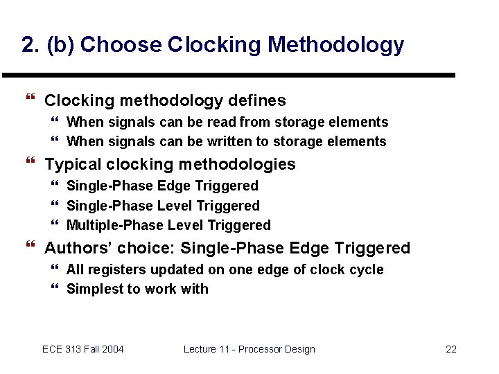
2. (b) Choose Clocking Methodology } Clocking methodology defines } When signals can be read from storage elements } When signals can be written to storage elements } Typical clocking methodologies } Single-Phase Edge Triggered } Single-Phase Level Triggered } Multiple-Phase Level Triggered } Authors’ choice: Single-Phase Edge Triggered } All registers updated on one edge of clock cycle } Simplest to work with ECE 313 Fall 2004 Lecture 11 - Processor Design 22

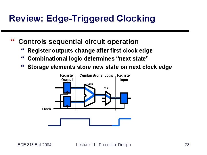
Review: Edge-Triggered Clocking } Controls sequential circuit operation } Register outputs change after first clock edge } Combinational logic determines “next state” } Storage elements store new state on next clock edge Register Output Combinational Logic Register Input Adder Mux Clock ECE 313 Fall 2004 Lecture 11 - Processor Design 23

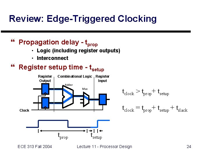
Review: Edge-Triggered Clocking } Propagation delay - tprop • Logic (including register outputs) • Interconnect } Register setup time - tsetup Register Output Combinational Logic Register Input Adder tclock > tprop+ tsetup Mux tclock = tprop+ tsetup + tslack Clock tprop ECE 313 Fall 2004 tsetup Lecture 11 - Processor Design 24

Outline - Processor Implementation } Overview } Single-Cycle Implementation 1. Analyze instruction set; get datapath requirements 2. Select datapath components and establish clocking methodology 3. Assemble datapath that meets requirements 4. Determine control signal values for each instruction 5. Assemble control logic to generate control signals } Multi-Cycle Implementation } Pipelined Implementation ECE 313 Fall 2004 Lecture 11 - Processor Design 25

3. Assemble Datapath } Tasks processor must implement 1. Fetch Instruction from memory 2. Decode Instruction, read register values 3. If necessary, perform an ALU operation 4. If memory address, perform load/store 5. Write results back to register file and increment PC } How can we do this with the datapath hardware? ECE 313 Fall 2004 Lecture 11 - Processor Design 26
![Datapath for Instruction Fetch Instruction MEMPC PC PC 4 ECE 313 Datapath for Instruction Fetch Instruction <- MEM[PC] PC <- PC + 4 ECE 313](https://slidetodoc.com/presentation_image_h2/f32e0b3e2c8098475ca06d59e2c3f5ba/image-27.jpg)
Datapath for Instruction Fetch Instruction <- MEM[PC] PC <- PC + 4 ECE 313 Fall 2004 Lecture 11 - Processor Design 27
![Datapath for RType Instructions add rd rs rt Rrd Rrs Rrt ECE Datapath for R-Type Instructions add rd, rs, rt R[rd] <- R[rs] + R[rt]; ECE](https://slidetodoc.com/presentation_image_h2/f32e0b3e2c8098475ca06d59e2c3f5ba/image-28.jpg)
Datapath for R-Type Instructions add rd, rs, rt R[rd] <- R[rs] + R[rt]; ECE 313 Fall 2004 Lecture 11 - Processor Design 28
![Datapath for LoadStore Instructions lw rt offsetrs Rrt MEMRrs sextendoffset ECE 313 Datapath for Load/Store Instructions lw rt, offset(rs) R[rt] <- MEM[R[rs] + s_extend(offset)]; ECE 313](https://slidetodoc.com/presentation_image_h2/f32e0b3e2c8098475ca06d59e2c3f5ba/image-29.jpg)
Datapath for Load/Store Instructions lw rt, offset(rs) R[rt] <- MEM[R[rs] + s_extend(offset)]; ECE 313 Fall 2004 Lecture 11 - Processor Design 29
![Datapath for LoadStore Instructions sw rt offsetrs MEMRrs signextendoffset Rrt ECE 313 Datapath for Load/Store Instructions sw rt, offset(rs) MEM[R[rs] + sign_extend(offset)] <- R[rt] ECE 313](https://slidetodoc.com/presentation_image_h2/f32e0b3e2c8098475ca06d59e2c3f5ba/image-30.jpg)
Datapath for Load/Store Instructions sw rt, offset(rs) MEM[R[rs] + sign_extend(offset)] <- R[rt] ECE 313 Fall 2004 Lecture 11 - Processor Design 30
![Datapath for Branch Instructions beq rs rt offset if Rrs Rrt then PC Datapath for Branch Instructions beq rs, rt, offset if (R[rs] == R[rt]) then PC](https://slidetodoc.com/presentation_image_h2/f32e0b3e2c8098475ca06d59e2c3f5ba/image-31.jpg)
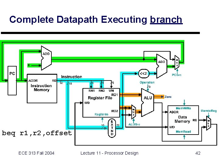
Datapath for Branch Instructions beq rs, rt, offset if (R[rs] == R[rt]) then PC <- PC+4 + s_extend(offset<<2) ECE 313 Fall 2004 Lecture 11 - Processor Design 31

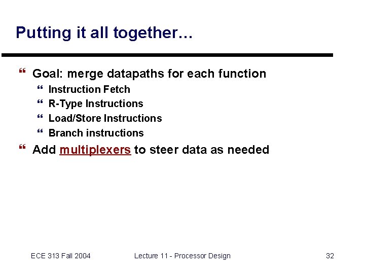
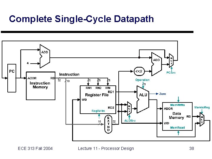
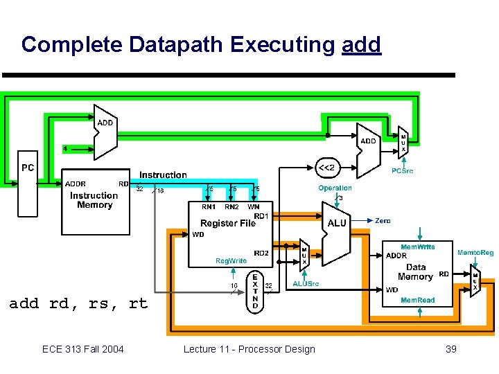
Putting it all together… } Goal: merge datapaths for each function } } Instruction Fetch R-Type Instructions Load/Store Instructions Branch instructions } Add multiplexers to steer data as needed ECE 313 Fall 2004 Lecture 11 - Processor Design 32

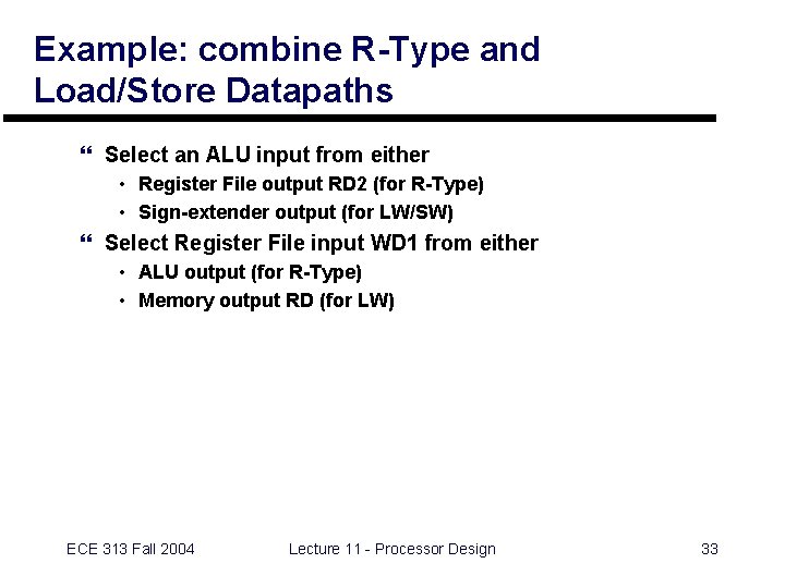
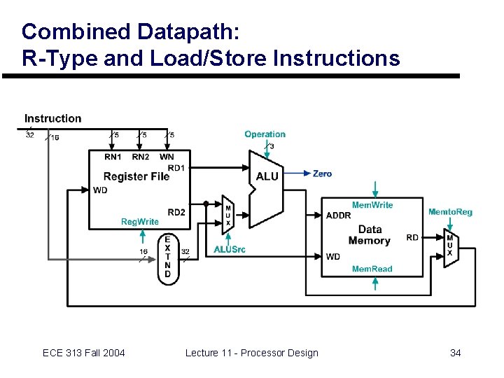
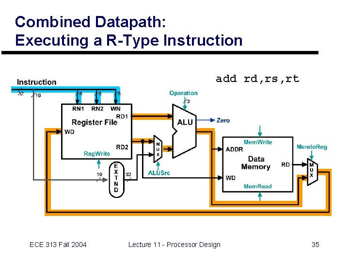
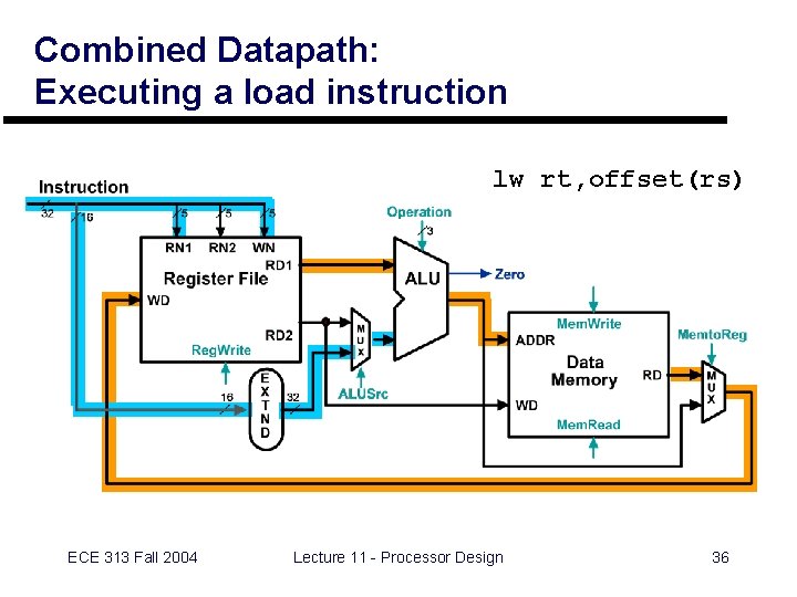
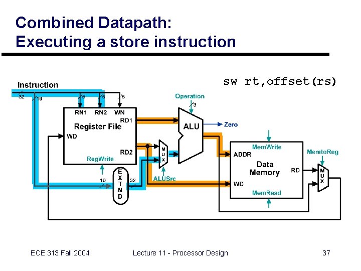
Example: combine R-Type and Load/Store Datapaths } Select an ALU input from either • Register File output RD 2 (for R-Type) • Sign-extender output (for LW/SW) } Select Register File input WD 1 from either • ALU output (for R-Type) • Memory output RD (for LW) ECE 313 Fall 2004 Lecture 11 - Processor Design 33

Combined Datapath: R-Type and Load/Store Instructions ECE 313 Fall 2004 Lecture 11 - Processor Design 34

Combined Datapath: Executing a R-Type Instruction add rd, rs, rt ECE 313 Fall 2004 Lecture 11 - Processor Design 35

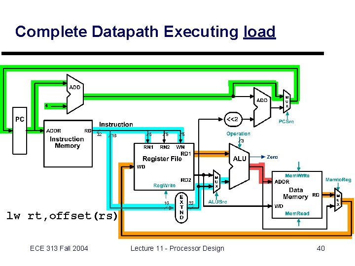
Combined Datapath: Executing a load instruction lw rt, offset(rs) ECE 313 Fall 2004 Lecture 11 - Processor Design 36

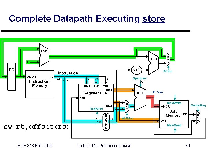
Combined Datapath: Executing a store instruction sw rt, offset(rs) ECE 313 Fall 2004 Lecture 11 - Processor Design 37

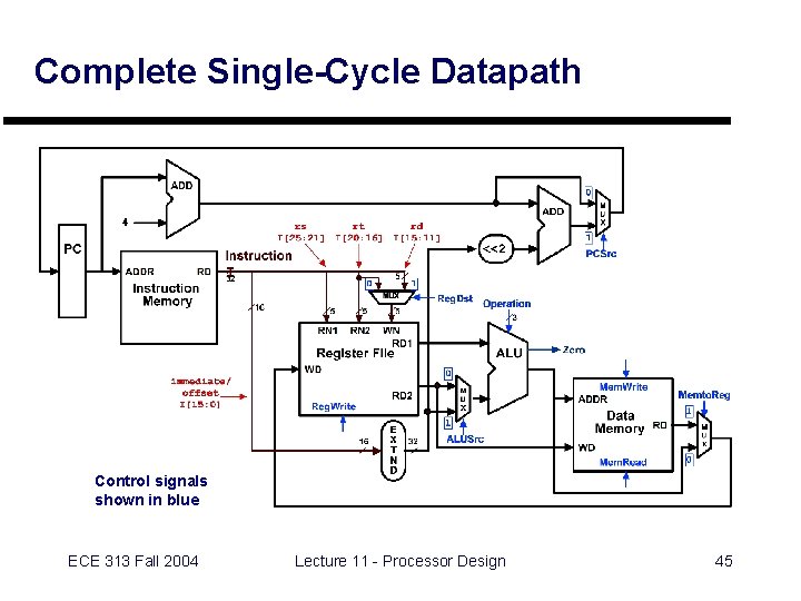
Complete Single-Cycle Datapath ECE 313 Fall 2004 Lecture 11 - Processor Design 38

Complete Datapath Executing add rd, rs, rt ECE 313 Fall 2004 Lecture 11 - Processor Design 39

Complete Datapath Executing load lw rt, offset(rs) ECE 313 Fall 2004 Lecture 11 - Processor Design 40

Complete Datapath Executing store sw rt, offset(rs) ECE 313 Fall 2004 Lecture 11 - Processor Design 41

Complete Datapath Executing branch beq r 1, r 2, offset ECE 313 Fall 2004 Lecture 11 - Processor Design 42

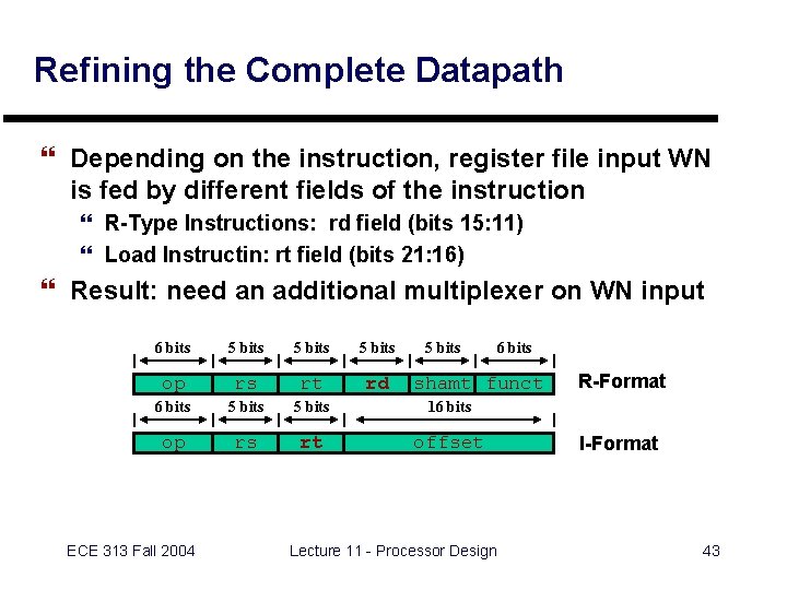
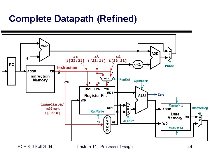
Refining the Complete Datapath } Depending on the instruction, register file input WN is fed by different fields of the instruction } R-Type Instructions: rd field (bits 15: 11) } Load Instructin: rt field (bits 21: 16) } Result: need an additional multiplexer on WN input 6 bits 5 bits op rs rt rd 6 bits 5 bits 16 bits op rs rt offset ECE 313 Fall 2004 5 bits 6 bits shamt funct Lecture 11 - Processor Design R-Format I-Format 43

Complete Datapath (Refined) ECE 313 Fall 2004 Lecture 11 - Processor Design 44

Complete Single-Cycle Datapath Control signals shown in blue ECE 313 Fall 2004 Lecture 11 - Processor Design 45

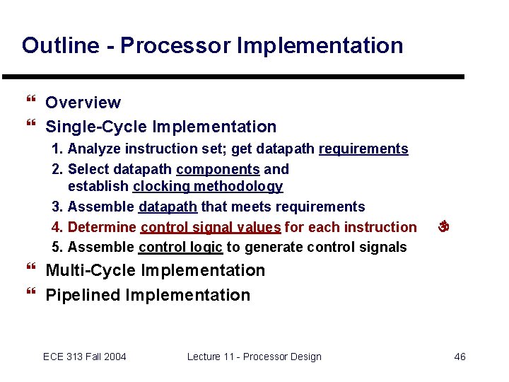
Outline - Processor Implementation } Overview } Single-Cycle Implementation 1. Analyze instruction set; get datapath requirements 2. Select datapath components and establish clocking methodology 3. Assemble datapath that meets requirements 4. Determine control signal values for each instruction 5. Assemble control logic to generate control signals } Multi-Cycle Implementation } Pipelined Implementation ECE 313 Fall 2004 Lecture 11 - Processor Design 46

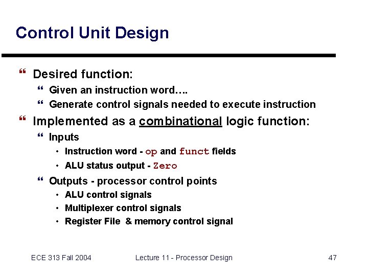
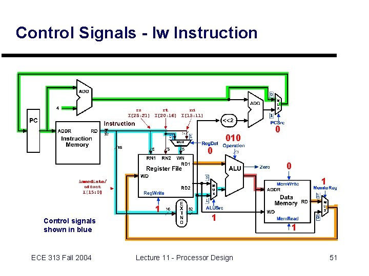
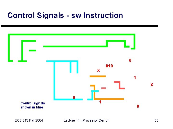
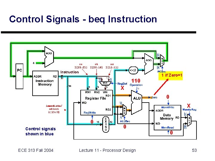
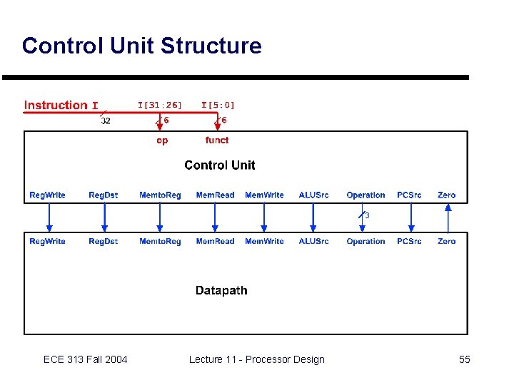
Control Unit Design } Desired function: } Given an instruction word…. } Generate control signals needed to execute instruction } Implemented as a combinational logic function: } Inputs • Instruction word - op and funct fields • ALU status output - Zero } Outputs - processor control points • ALU control signals • Multiplexer control signals • Register File & memory control signal ECE 313 Fall 2004 Lecture 11 - Processor Design 47

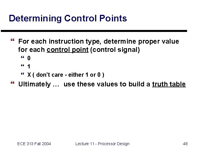
Determining Control Points } For each instruction type, determine proper value for each control point (control signal) } 0 } 1 } X ( don’t care - either 1 or 0 ) } Ultimately … use these values to build a truth table ECE 313 Fall 2004 Lecture 11 - Processor Design 48

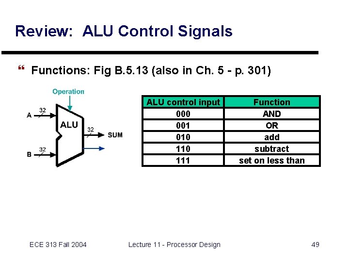
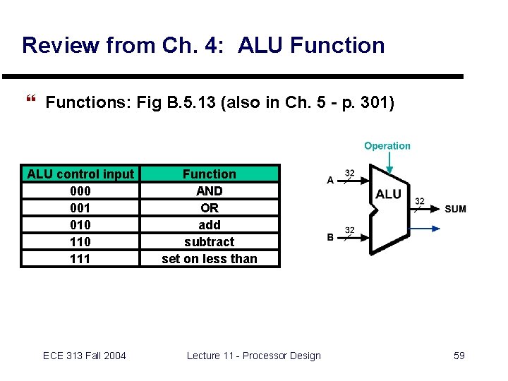
Review: ALU Control Signals } Functions: Fig B. 5. 13 (also in Ch. 5 - p. 301) ALU control input 000 001 010 111 ECE 313 Fall 2004 Lecture 11 - Processor Design Function AND OR add subtract set on less than 49

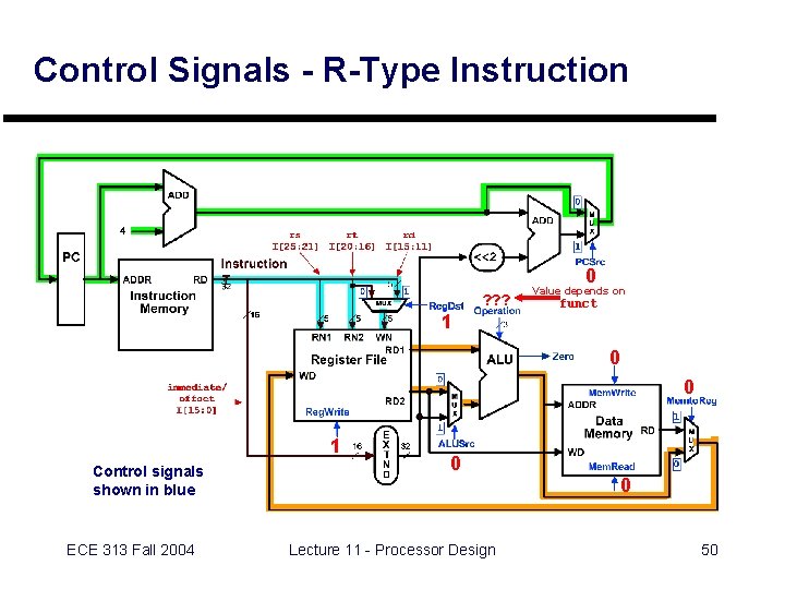
Control Signals - R-Type Instruction 0 ? ? ? 1 Value depends on funct 0 0 1 Control signals shown in blue ECE 313 Fall 2004 0 0 Lecture 11 - Processor Design 50

Control Signals - lw Instruction 010 0 1 1 Control signals shown in blue ECE 313 Fall 2004 1 Lecture 11 - Processor Design 1 51

Control Signals - sw Instruction 0 X 010 1 X 0 Control signals shown in blue ECE 313 Fall 2004 1 Lecture 11 - Processor Design 0 52

Control Signals - beq Instruction 1 if Zero=1 110 X 0 Control signals shown in blue ECE 313 Fall 2004 0 0 Lecture 11 - Processor Design 53

Outline - Processor Implementation } Overview } Single-Cycle Implementation 1. Analyze instruction set; get datapath requirements 2. Select datapath components and establish clocking methodology 3. Assemble datapath that meets requirements 4. Determine control signal values for each instruction 5. Assemble control logic to generate control signals } Multi-Cycle Implementation } Pipelined Implementation ECE 313 Fall 2004 Lecture 11 - Processor Design 54

Control Unit Structure ECE 313 Fall 2004 Lecture 11 - Processor Design 55

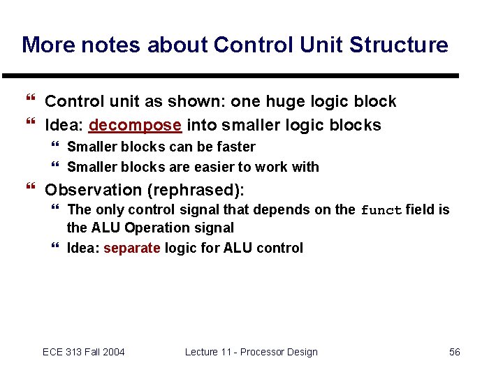
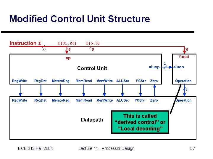
More notes about Control Unit Structure } Control unit as shown: one huge logic block } Idea: decompose into smaller logic blocks } Smaller blocks can be faster } Smaller blocks are easier to work with } Observation (rephrased): } The only control signal that depends on the funct field is the ALU Operation signal } Idea: separate logic for ALU control ECE 313 Fall 2004 Lecture 11 - Processor Design 56

Modified Control Unit Structure This is called “derived control” or “Local decoding” ECE 313 Fall 2004 Lecture 11 - Processor Design 57

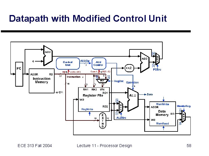
Datapath with Modified Control Unit ECE 313 Fall 2004 Lecture 11 - Processor Design 58

Review from Ch. 4: ALU Function } Functions: Fig B. 5. 13 (also in Ch. 5 - p. 301) ALU control input 000 001 010 111 ECE 313 Fall 2004 Function AND OR add subtract set on less than Lecture 11 - Processor Design 59

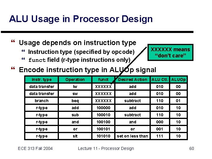
ALU Usage in Processor Design } Usage depends on instruction type } Instruction type (specified by opcode) } funct field (r-type instructions only) XXXXXX means “don’t care” } Encode instruction type in ALUOp signal Instr. type Operation funct Desired Action data transfer lw XXXXXX add 010 00 data transfer sw XXXXXX add 010 00 branch beq XXXXXX subtract 110 01 r-type add 100000 add 010 10 r-type sub 100010 subtract 110 10 r-type and 100100 and 000 10 r-type or 100101 or 001 10 r-type slt 101010 set on less than 111 10 ECE 313 Fall 2004 Lecture 11 - Processor Design ALU Ctl. ALUOp 60

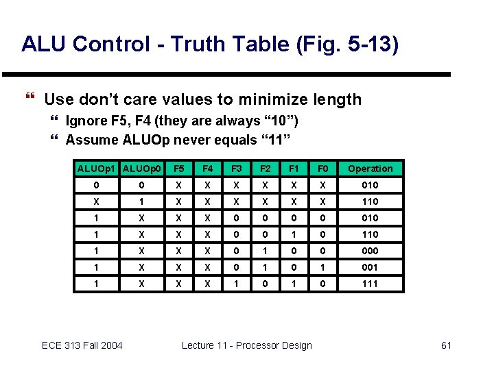
ALU Control - Truth Table (Fig. 5 -13) } Use don’t care values to minimize length } Ignore F 5, F 4 (they are always “ 10”) } Assume ALUOp never equals “ 11” ALUOp 1 ALUOp 0 F 5 F 4 F 3 F 2 F 1 F 0 Operation 0 0 X X X 010 X 1 X X X 110 1 X X X 0 0 010 1 X X X 0 0 110 1 X X X 0 1 0 0 000 1 X X X 0 1 001 1 X X X 1 0 111 ECE 313 Fall 2004 Lecture 11 - Processor Design 61

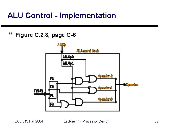
ALU Control - Implementation } Figure C. 2. 3, page C-6 ECE 313 Fall 2004 Lecture 11 - Processor Design 62

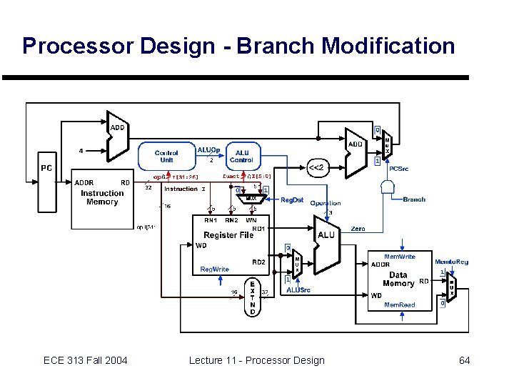
One More Modification - for Branch } BEQ instruction depends on Zero output of ALU } No other instruction uses Zero output } Local decoding } Implement with new "Branch" control signal } Add AND gate to generate PCSelect ECE 313 Fall 2004 Lecture 11 - Processor Design 63

Processor Design - Branch Modification ECE 313 Fall 2004 Lecture 11 - Processor Design 64

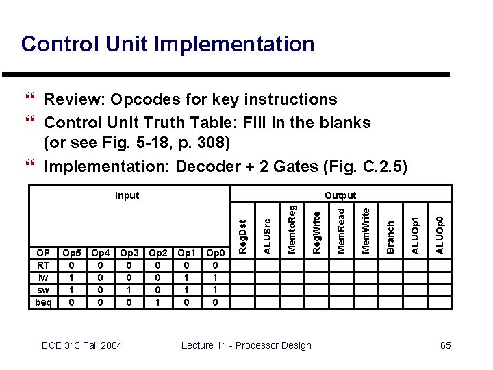
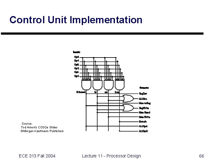
Control Unit Implementation } Review: Opcodes for key instructions } Control Unit Truth Table: Fill in the blanks (or see Fig. 5 -18, p. 308) } Implementation: Decoder + 2 Gates (Fig. C. 2. 5) ECE 313 Fall 2004 Lecture 11 - Processor Design ALUOp 0 ALUOp 1 Op 0 0 1 1 0 Branch Op 1 0 1 1 0 Mem. Write Op 2 0 0 0 1 Mem. Read Op 3 0 0 1 0 Reg. Write Op 4 0 0 Memto. Reg Op 5 0 1 1 0 ALUSrc OP RT lw sw beq Output Reg. Dst Input 65

Control Unit Implementation Source: Tod Amon's COD 2 e Slides ©Morgan Kaufmann Publishers ECE 313 Fall 2004 Lecture 11 - Processor Design 66

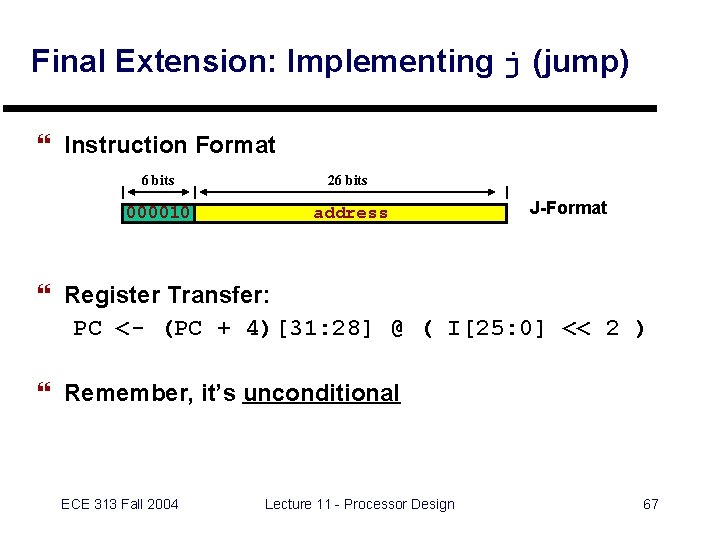
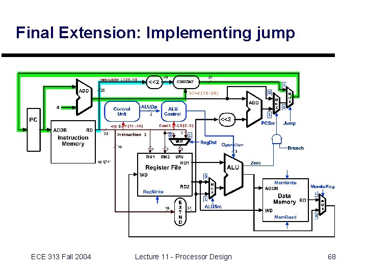
Final Extension: Implementing j (jump) } Instruction Format 6 bits 26 bits 000010 address J-Format } Register Transfer: PC <- (PC + 4)[31: 28] @ ( I[25: 0] << 2 ) } Remember, it’s unconditional ECE 313 Fall 2004 Lecture 11 - Processor Design 67

Final Extension: Implementing jump ECE 313 Fall 2004 Lecture 11 - Processor Design 68

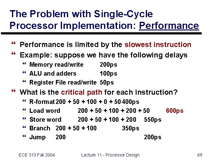
The Problem with Single-Cycle Processor Implementation: Performance } Performance is limited by the slowest instruction } Example: suppose we have the following delays } Memory read/write 200 ps } ALU and adders 100 ps } Register File read/write 50 ps } What is the critical path for each instruction? } } } R-format 200 + 50 + 100 + 50 400 ps Load word 200 + 50 + 100 + 200 + 50 600 ps Store word 200 + 50 + 100 + 200 550 ps Branch 200 + 50 + 100 350 ps Jump 200 ps ECE 313 Fall 2004 Lecture 11 - Processor Design 69

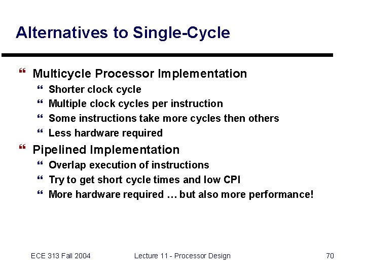
Alternatives to Single-Cycle } Multicycle Processor Implementation } } Shorter clock cycle Multiple clock cycles per instruction Some instructions take more cycles then others Less hardware required } Pipelined Implementation } Overlap execution of instructions } Try to get short cycle times and low CPI } More hardware required … but also more performance! ECE 313 Fall 2004 Lecture 11 - Processor Design 70

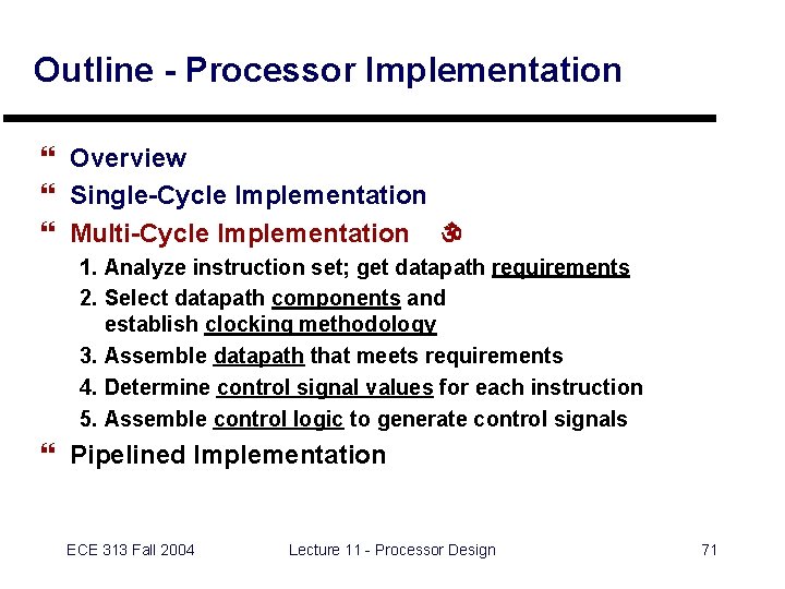
Outline - Processor Implementation } Overview } Single-Cycle Implementation } Multi-Cycle Implementation 1. Analyze instruction set; get datapath requirements 2. Select datapath components and establish clocking methodology 3. Assemble datapath that meets requirements 4. Determine control signal values for each instruction 5. Assemble control logic to generate control signals } Pipelined Implementation ECE 313 Fall 2004 Lecture 11 - Processor Design 71