ECE 313 Computer Organization MultiCycle Processor Design 2
![Example Problem: Datapath 3 2 1 0 Reg[rs] What needs to be changed? Fall Example Problem: Datapath 3 2 1 0 Reg[rs] What needs to be changed? Fall](https://slidetodoc.com/presentation_image_h2/a74c4187181febd77ff46851fb5dec28/image-13.jpg)
- Slides: 28

ECE 313 - Computer Organization Multi-Cycle Processor Design 2 Fall 2005 Reading: 5. 6 - 5. 11, C. 4 - C. 5 HW Due Fri. 5/11: 5. 32, 5. 34, 5. 35, 5. 47, 5. 49, 5. 55 Prof. John Nestor ECE Department Lafayette College Easton, Pennsylvania 18042 nestorj@lafayette. edu Portions of these slides are derived from: Textbook figures © 1998 Morgan Kaufmann Publishers all rights reserved Tod Amon's COD 2 e Slides © 1998 Morgan Kaufmann Publishers all rights reserved Dave Patterson’s CS 152 Slides - Fall 1997 © UCB Rob Rutenbar’s 18 -347 Slides - Fall 1999 CMU Fall 2005 Multicycle Design 2 other sources as noted 1

Outline - Multicycle Design } } } } Overview Datapath Design Controller Design Aside: FSM Design in Verilog Performance Considerations Extending the Design: An Example Microprogramming Exceptions Fall 2005 Multicycle Design 2 2

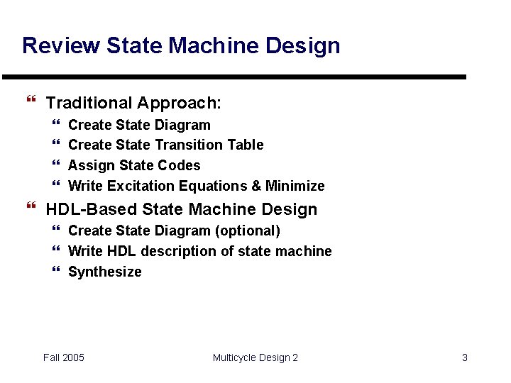
Review State Machine Design } Traditional Approach: } } Create State Diagram Create State Transition Table Assign State Codes Write Excitation Equations & Minimize } HDL-Based State Machine Design } Create State Diagram (optional) } Write HDL description of state machine } Synthesize Fall 2005 Multicycle Design 2 3

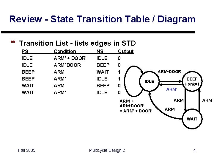
Review - State Transition Table / Diagram } Transition List - lists edges in STD PS IDLE BEEP WAIT Condition ARM' + DOOR' ARM*DOOR ARM ARM' NS IDLE BEEP WAIT IDLE BEEP IDLE Output 0 0 1 1 0 0 ARM • DOOR BEEP Honk=1 IDLE ARM’ + ARM • DOOR’ = ARM’ + DOOR’ ARM ARM’ WAIT Fall 2005 Multicycle Design 2 4

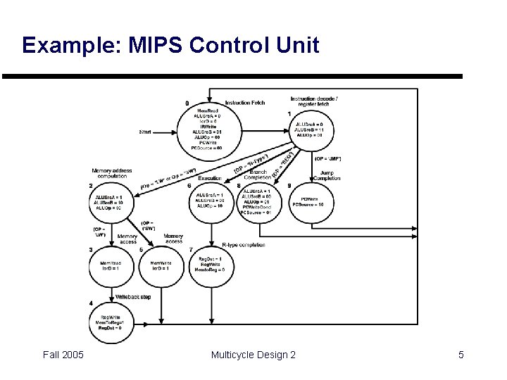
Example: MIPS Control Unit Fall 2005 Multicycle Design 2 5

Review: Full Multicycle Implementation Fall 2005 Multicycle Design 2 6

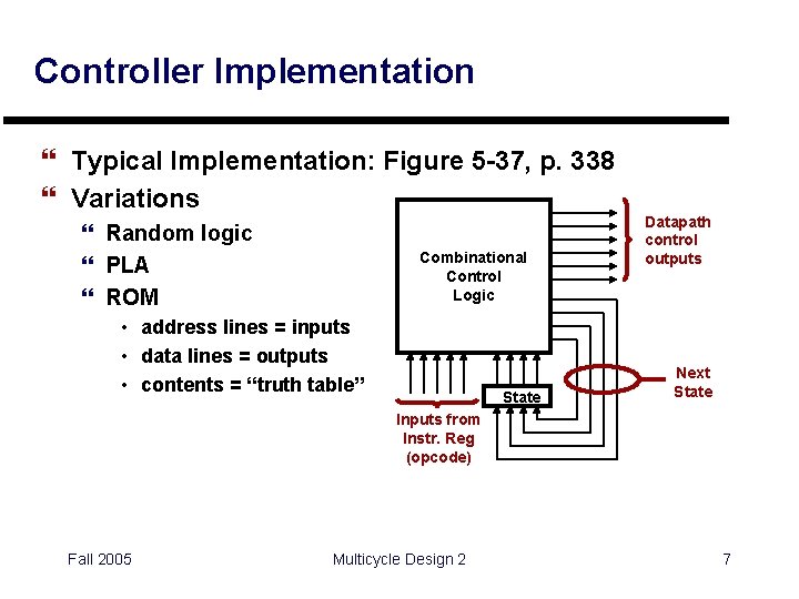
Controller Implementation } Typical Implementation: Figure 5 -37, p. 338 } Variations } Random logic } PLA } ROM Combinational Control Logic • address lines = inputs • data lines = outputs • contents = “truth table” State Datapath control outputs Next State Inputs from Instr. Reg (opcode) Fall 2005 Multicycle Design 2 7

Outline - Multicycle Design } } } } Overview Datapath Design Controller Design Aside: FSM Design in Verilog Performance Considerations Extending the Design: An Example Microprogramming Exceptions Fall 2005 Multicycle Design 2 8

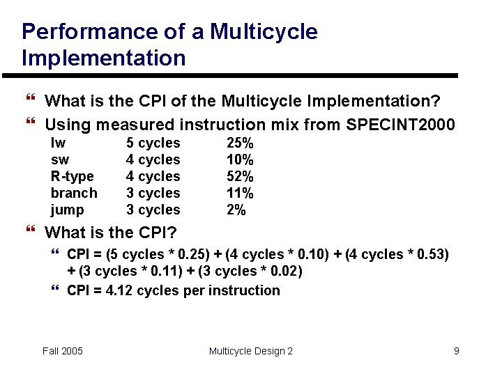
Performance of a Multicycle Implementation } What is the CPI of the Multicycle Implementation? } Using measured instruction mix from SPECINT 2000 lw sw R-type branch jump 5 cycles 4 cycles 3 cycles 25% 10% 52% 11% 2% } What is the CPI? } CPI = (5 cycles * 0. 25) + (4 cycles * 0. 10) + (4 cycles * 0. 53) + (3 cycles * 0. 11) + (3 cycles * 0. 02) } CPI = 4. 12 cycles per instruction Fall 2005 Multicycle Design 2 9

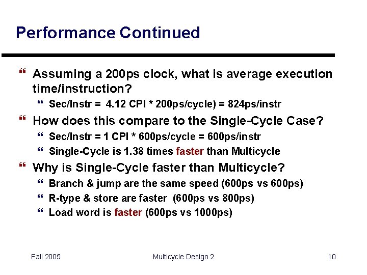
Performance Continued } Assuming a 200 ps clock, what is average execution time/instruction? } Sec/Instr = 4. 12 CPI * 200 ps/cycle) = 824 ps/instr } How does this compare to the Single-Cycle Case? } Sec/Instr = 1 CPI * 600 ps/cycle = 600 ps/instr } Single-Cycle is 1. 38 times faster than Multicycle } Why is Single-Cycle faster than Multicycle? } Branch & jump are the same speed (600 ps vs 600 ps) } R-type & store are faster (600 ps vs 800 ps) } Load word is faster (600 ps vs 1000 ps) Fall 2005 Multicycle Design 2 10

Outline - Multicycle Design } } } } Overview Datapath Design Controller Design Aside: FSM Design in Verilog Performance Considerations Extending the Design: An Example Microprogramming Exceptions Fall 2005 Multicycle Design 2 11

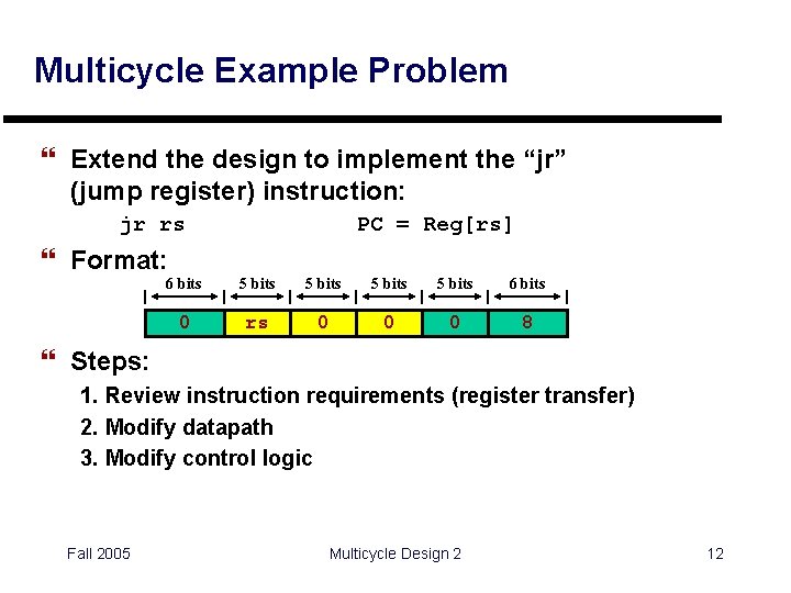
Multicycle Example Problem } Extend the design to implement the “jr” (jump register) instruction: jr rs PC = Reg[rs] } Format: 6 bits 5 bits 6 bits 0 rs 0 0 0 8 } Steps: 1. Review instruction requirements (register transfer) 2. Modify datapath 3. Modify control logic Fall 2005 Multicycle Design 2 12
![Example Problem Datapath 3 2 1 0 Regrs What needs to be changed Fall Example Problem: Datapath 3 2 1 0 Reg[rs] What needs to be changed? Fall](https://slidetodoc.com/presentation_image_h2/a74c4187181febd77ff46851fb5dec28/image-13.jpg)
Example Problem: Datapath 3 2 1 0 Reg[rs] What needs to be changed? Fall 2005 Multicycle Design 2 13

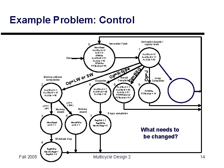
Example Problem: Control Mem. Read ALUSrc. A = 0 Ior. D = 0 IRWrite ALUSrc. B = 01 ALUOp = 00 PCWrite PCSource = 00 2 ALUSrc. A = 0 ALUSrc. B = 11 ALUOp = 00 Execution 6 8 Branch Completion ALUSrc. A = 1 ALUSrc. B = 00 ALUOp = 01 PCWrite. Cond PCSource = 01 ALUSrc. A = 1 ALUSrc. B = 00 ALUOp = 10 Op=J L Op= Op (OP = ‘JR‘) ype t R =B EQ = W r. S Wo ALUSrc. A = 1 ALUSrc. B = 10 ALUOp = 00 (OP = ‘LW’) 1 Op Start Memory address computation Instruction decode / register fetch Instruction Fetch 0 Jump Completion 9 PCWrite PCSource = 10 PCWrite PCSource = 11 (OP = (‘SW’) Memory access 3 5 Mem. Read Ior. D = 1 7 Mem. Write Ior. D = 1 R-type completion Reg. Dst = 1 Reg. Write Memto. Reg = 0 Writeback step What needs to be changed? 4 Fall 2005 Reg. Write Mem. To. Reg=1 Reg. Dst = 0 Multicycle Design 2 14

Outline - Multicycle Design } } } } Overview Datapath Design Controller Design Aside: FSM Design in Verilog Performance Considerations Extending the Design: An Example Microprogramming Exceptions Fall 2005 Multicycle Design 2 15

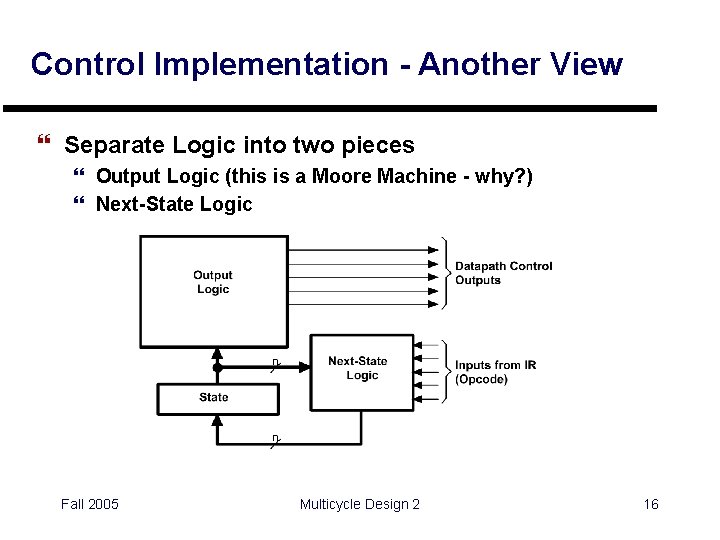
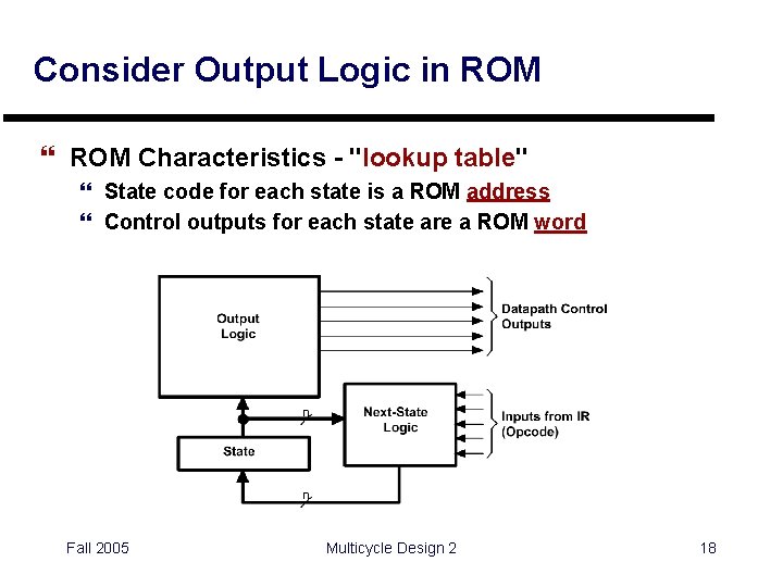
Control Implementation - Another View } Separate Logic into two pieces } Output Logic (this is a Moore Machine - why? ) } Next-State Logic Fall 2005 Multicycle Design 2 16

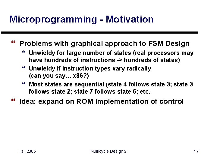
Microprogramming - Motivation } Problems with graphical approach to FSM Design } Unwieldy for large number of states (real processors may have hundreds of instructions -> hundreds of states) } Unwieldy if instruction types vary radically (can you say… x 86? ) } Most states are sequential (state 4 follows state 3; state 3 follows state 2; state 7 follows state 6; etc. } Idea: expand on ROM implementation of control Fall 2005 Multicycle Design 2 17

Consider Output Logic in ROM } ROM Characteristics - "lookup table" } State code for each state is a ROM address } Control outputs for each state are a ROM word Fall 2005 Multicycle Design 2 18

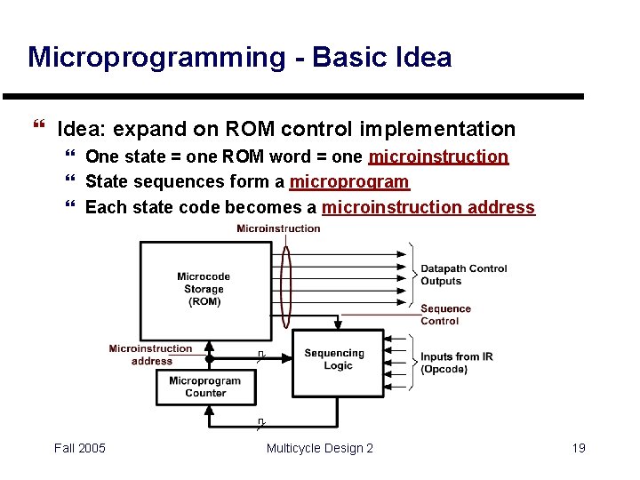
Microprogramming - Basic Idea } Idea: expand on ROM control implementation } One state = one ROM word = one microinstruction } State sequences form a microprogram } Each state code becomes a microinstruction address Fall 2005 Multicycle Design 2 19

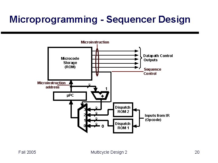
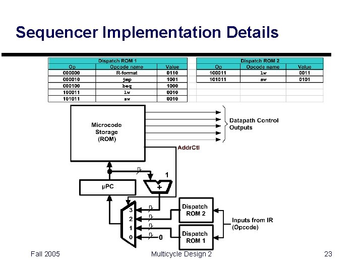
Microprogramming - Sequencer Design Microinstruction Datapath Control Outputs Microcode Storage (ROM) Sequence Control Microinstruction address n 1 + µPC 3 2 1 0 Fall 2005 n n Dispatch ROM 2 0 Dispatch ROM 1 Multicycle Design 2 Inputs from IR (Opcode) 20

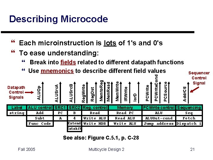
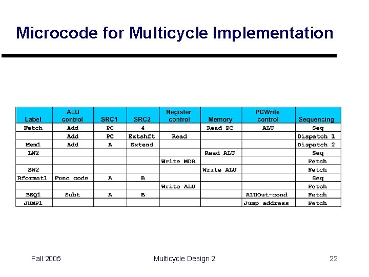
Describing Microcode } Each microinstruction is lots of 1's and 0's } To ease understanding: Label ALU control SRC 1 SRC 2 Reg. control string Add PC B Read Subt A 4 Write ALU Extend Write MDR Func Code Memory Read PC Read ALU Write ALU Sequencer Control Signal Addr. Ctl PCSource PCWrite. Cond PCWrite Ior. D IRWrite Mem. Read Memto. Reg. Dst Reg. Write ALUSrc. B ALUSrc. A Datapath Control Signals ALUOp } Break into fields related to different datapath functions } Use mnemonics to describe different field values PCWrite control Sequencing ALU Seq ALUOut-cond Fetch Jump address Dispatch i Extshft See also: Figure C. 5. 1, p. C-28 Fall 2005 Multicycle Design 2 21

Microcode for Multicycle Implementation Fall 2005 Multicycle Design 2 22

Sequencer Implementation Details Fall 2005 Multicycle Design 2 23

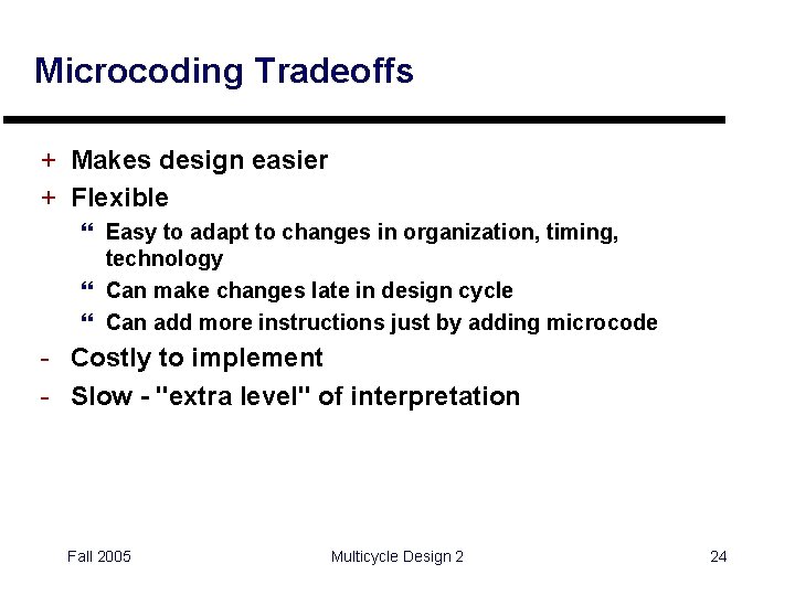
Microcoding Tradeoffs + Makes design easier + Flexible } Easy to adapt to changes in organization, timing, technology } Can make changes late in design cycle } Can add more instructions just by adding microcode - Costly to implement - Slow - "extra level" of interpretation Fall 2005 Multicycle Design 2 24

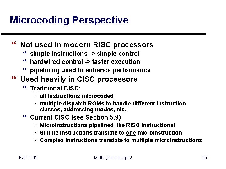
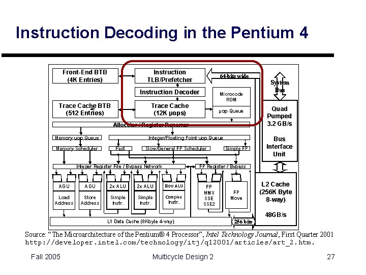
Microcoding Perspective } Not used in modern RISC processors } simple instructions -> simple control } hardwired control -> faster execution } pipelining used to enhance performance } Used heavily in CISC processors } Traditional CISC: • all instructions microcoded • multiple dispatch ROMs to handle different instruction classes, addressing modes, etc. } Current CISC (see Section 5. 9) • Microinstructions pipelined like RISC instructions! • Simple instructions translate to one microinstruction • Complex instructions translate to multiple microinstructions Fall 2005 Multicycle Design 2 25

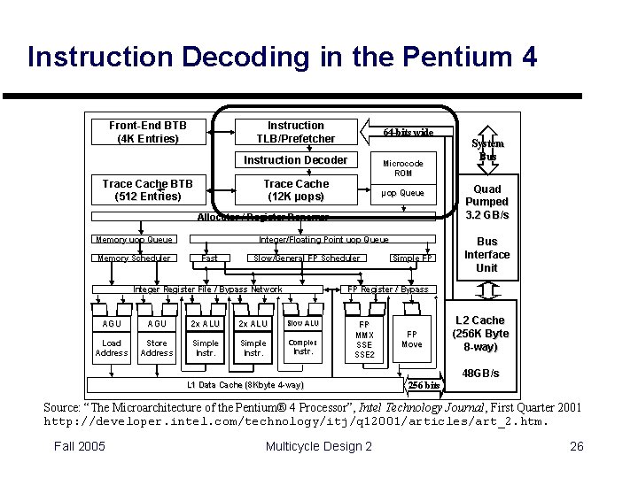
Instruction Decoding in the Pentium 4 Source: “The Microarchitecture of the Pentium® 4 Processor”, Intel Technology Journal, First Quarter 2001 http: //developer. intel. com/technology/itj/q 12001/articles/art_2. htm. Fall 2005 Multicycle Design 2 26

Instruction Decoding in the Pentium 4 Source: “The Microarchitecture of the Pentium® 4 Processor”, Intel Technology Journal, First Quarter 2001 http: //developer. intel. com/technology/itj/q 12001/articles/art_2. htm. Fall 2005 Multicycle Design 2 27

Coming Up } Implementing Exceptions } Pipelined Design Fall 2005 Multicycle Design 2 28