Processor Organization UNIT No 5 Processor Organization Requirement


. •")


 - this flag is set to 1 when there")


- Slides: 50
Processor Organization UNIT No 5
Processor Organization • Requirement placed on the Processor • Fetch instruction: The processor reads an instruction from memory (register, cache, main memory). • Interpret instruction: The instruction is decoded to determine what action is required. • Fetch data: The execution of an instruction may require reading data from memory or an I/O module. • Process data: The execution of an instruction may require performing some arithmetic or logical operation on data. • Write data: The results of an execution may require writing data to memory or an I/O module.
CPU with System Bus
Internal structure of the cpu
Pin out 8086
• Power supply and frequency signals • It uses 5 V DC supply at VCC pin 40, and uses ground at VSS pin 1 and 20 for its operation. • Clock signal is provided through Pin-19. It provides timing to the processor for operations. Its frequency is different for different versions, i. e. 5 MHz, 8 MHz and 10 MHz. • Address/data bus • AD 0 -AD 15. These are 16 address/data bus. AD 0 -AD 7 carries low order byte data and AD 8 AD 15 carries higher order byte data. During the first clock cycle, it carries 16 -bit address and after that it carries 16 -bit data. • Address/status bus • A 16 -A 19/S 3 -S 6. These are the 4 address/status buses. During the first clock cycle, it carries 4 -bit address and later it carries status signals.
• • • S 7/BHE stands for Bus High Enable. It is available at pin 34 and used to indicate the transfer of data using data bus D 8 -D 15. This signal is low during the first clock cycle, thereafter it is active. Read($overline{RD}$) It is available at pin 32 and is used to read signal for Read operation. Ready It is available at pin 32. It is an acknowledgement signal from I/O devices that data is transferred. It is an active high signal. When it is high, it indicates that the device is ready to transfer data. When it is low, it indicates wait state. RESET It is available at pin 21 and is used to restart the execution. It causes the processor to immediately terminate its present activity. This signal is active high for the first 4 clock cycles to RESET the microprocessor. INTR It is available at pin 18. It is an interrupt request signal, which is sampled during the last clock cycle of each instruction to determine if the processor considered this as an interrupt or not.
• NMI • It stands for non-maskable interrupt and is available at pin 17. It is an edge triggered input, which causes an interrupt request to the microprocessor. • $overline{TEST}$ • This signal is like wait state and is available at pin 23. When this signal is high, then the processor has to wait for IDLE state, else the execution continues.
• MN/$overline{MX}$ • It stands for Minimum/Maximum and is available at pin 33. It indicates what mode the processor is to operate in; when it is high, it works in the minimum mode and vice-aversa. • INTA • It is an interrupt acknowledgement signal and id available at pin 24. When the microprocessor receives this signal, it acknowledges the interrupt. • ALE • It stands for address enable latch and is available at pin 25. A positive pulse is generated each time the processor begins any operation. This signal indicates the availability of a valid address on the address/data lines. • DEN • It stands for Data Enable and is available at pin 26. It is used to enable Transreceiver 8286. The transreceiver is a device used to separate data from the address/data bus.
• • • DT/R It stands for Data Transmit/Receive signal and is available at pin 27. It decides the direction of data flow through the transreceiver. When it is high, data is transmitted out and vice-a-versa. M/IO This signal is used to distinguish between memory and I/O operations. When it is high, it indicates I/O operation and when it is low indicates the memory operation. It is available at pin 28. WR It stands for write signal and is available at pin 29. It is used to write the data into the memory or the output device depending on the status of M/IO signal. HLDA It stands for Hold Acknowledgement signal and is available at pin 30. This signal acknowledges the HOLD signal. HOLD This signal indicates to the processor that external devices are requesting to access the address/data buses. It is available at pin 31.
• S 0, S 1, S 2 • These are the status signals that provide the status of operation, which is used by the Bus Controller 8288 to generate memory & I/O control signals. These are available at pin 26, 27, and 28. Following is the table showing their status
• LOCK • When this signal is active, it indicates to the other processors not to ask the CPU to leave the system bus. It is activated using the LOCK prefix on any instruction and is available at pin 29. • RQ/GT 1 and RQ/GT 0 • These are the Request/Grant signals used by the other processors requesting the CPU to release the system bus. When the signal is received by CPU, then it sends acknowledgment. RQ/GT 0 has a higher priority than RQ/GT 1.
features • The most prominent features of a 8086 microprocessor are as follows − • It has an instruction queue, which is capable of storing six instruction bytes from the memory resulting in faster processing. • It was the first 16 -bit processor having 16 -bit ALU, 16 -bit registers, internal data bus, and 16 -bit external data bus resulting in faster processing. • It is available in 3 versions based on the frequency of operation − • 8086 → 5 MHz • 8086 -2 → 8 MHz • (c)8086 -1 → 10 MHz • It uses two stages of pipelining, i. e. Fetch Stage and Execute Stage, which improves performance.
• Fetch stage can prefectch up to 6 bytes of instructions and stores them in the queue. • Execute stage executes these instructions. • It has 256 vectored interrupts. • It consists of 29, 000 transistors.
8086 architecture diagram
Register set of 8086
Register Organization • Registers in processor perform two roles • User-visible registers: Enable the machine- or assembly language programmer to minimize main memory references by optimizing use of registers. • Control and status registers: Used by the control unit to control the operation of the processor and by privileged, operating system programs to control the execution of programs
User-Visible Registers characterize these in the following categories: • General purpose : uses as simple storage area, to store intermediate results • Data • Address • Condition codes
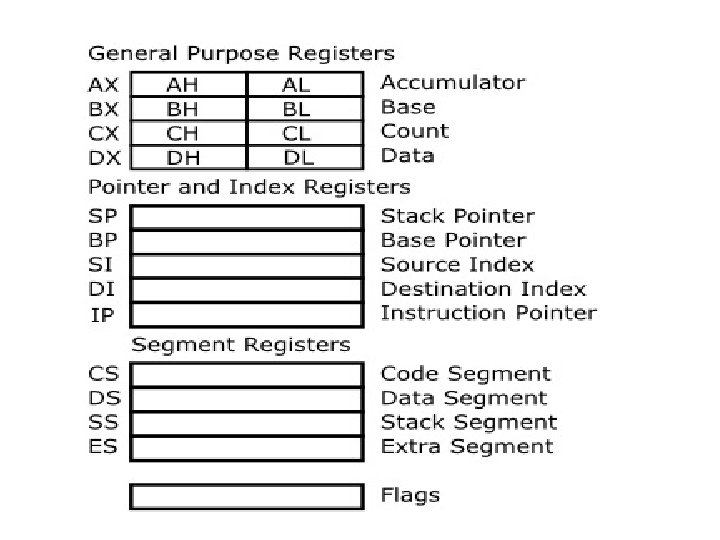
• GENERAL PURPOSE REGISTERS 8086 CPU has 8 general purpose registers, each register has its own name: • AX - the accumulator register (divided into AH / AL): – – – Generates shortest machine code Arithmetic, logic and data transfer One number must be in AL or AX Multiplication & Division Input & Output
• BX - the base address register (divided into BH / BL). • • CX - the count register (divided into CH / CL): – Iterative code segments using the LOOP instruction – Repetitive operations on strings with the REP command – Count (in CL) of bits to shift and rotate • • DX - the data register (divided into DH / DL): • – DX: AX concatenated into 32 -bit register for some MUL and DIV operations – Specifying ports in some IN and OUT operations
• SI - source index register: – Can be used for pointer addressing of data – Used as source in some string processing instructions – Offset address relative to DS • • DI - destination index register: – Can be used for pointer addressing of data – Used as destination in some string processing instructions – Offset address relative to ES • • BP - base pointer: – Primarily used to access parameters passed via the stack – Offset address relative to SS
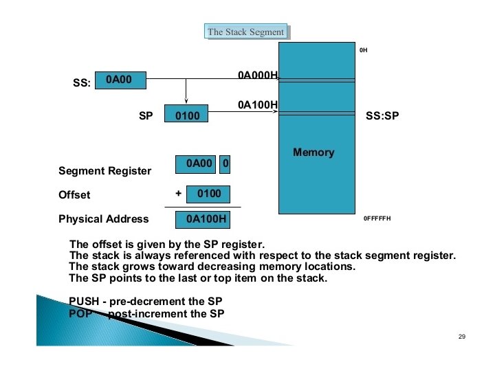
• SP - stack pointer: – Always points to top item on the stack – Offset address relative to SS – Always points to word) – An empty stack will had SP = FFFEh •
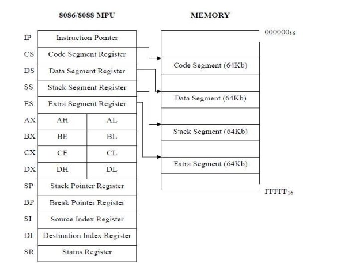
• SEGMENT REGISTERS • CS - points at the segment containing the current program. • DS - generally points at segment where variables are defined. • ES - extra segment register, it's up to a coder to define its usage. • SS - points at the segment containing the stack.
Segmented memory
• Segment registers work together with general purpose register to access any memory value. • For example if we would like to access memory at the physical address 12345 h (hexadecimal), we should set the DS = 1230 h and SI = 0045 h. This is good, since this way we can access much more memory than with a single register that is limited to 16 bit values. • CPU makes a calculation of physical address by multiplying the segment register by 10 h and adding general purpose register to it (1230 h * 10 h + 45 h = 12345 h):
• SPECIAL PURPOSE REGISTERS IP - the instruction pointer: – Always points to next instruction to be executed – Offset address relative to CS – CS: IP 2000 H X 10 H +IP = 20 bit address • IP register always works together with CS segment register and it points to currently executing instruction. •
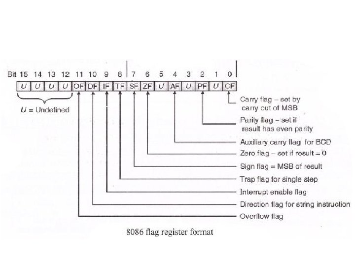
• FLAGS REGISTER • Flags Register - determines the current state of the processor. • Flags Register is modified automatically by CPU after mathematical operations, • this allows to determine the type of the result, and to determine conditions to transfer control to other parts of the program. Generally you cannot access these registers directly.
• Carry Flag (CF) - this flag is set to 1 when there is an unsigned overflow. For example when you add bytes 255 + 1 (result is not in range 0. . . 255). When there is no overflow this flag is set to 0. • Parity Flag (PF) - this flag is set to 1 when there is even number of one bits in result, and to 0 when there is odd number of one bits. Even if result is a word only 8 low bits are analyzed! • Auxiliary Flag (AF) - set to 1 when there is an unsigned overflow for low nibble (4 bits). • Zero Flag (ZF) - set to 1 when result is zero. For none zero result this flag is set to 0. • Sign Flag (SF) - set to 1 when result is negative. When result is positive it is set to 0. Actually this flag take the value of the most significant bit. • Trap Flag (TF) - Used for on-chip debugging. • Interrupt enable Flag (IF) - when this flag is set to 1 CPU reacts to interrupts from external devices. • Direction Flag (DF) - this flag is used by some instructions to process data chains, when this flag is set to 0 - the processing is done forward, when this flag is set to 1 the processing is done backward. • Overflow Flag (OF) - set to 1 when there is a signed overflow. For example, when you add bytes 100 + 50 (result is not in range -128. . . 127).
Timing diagram
Example Microprocessor register organization 386
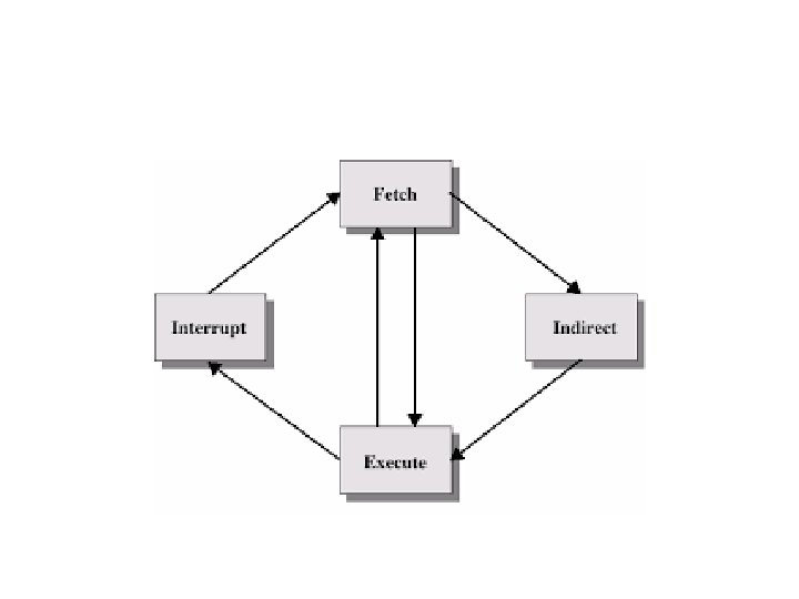
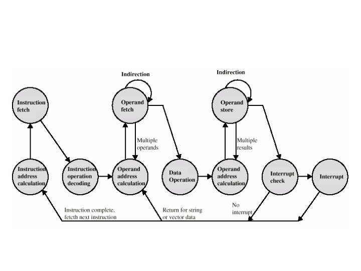
INSTRUCTION CYCLE an instruction cycle includes the following stages: • Fetch: Read the next instruction from memory into the processor. • Execute: Interpret the opcode and perform the indicated operation. • Interrupt: If interrupts are enabled an interrupt has occurred, save the current process state and service the interrupt.
• First, we must introduce one additional stage, known as the indirect cycle.
Data Flow Fetch Cycle
Data Flow Indirect Cycle
Data Flow, Interrupt Cycle
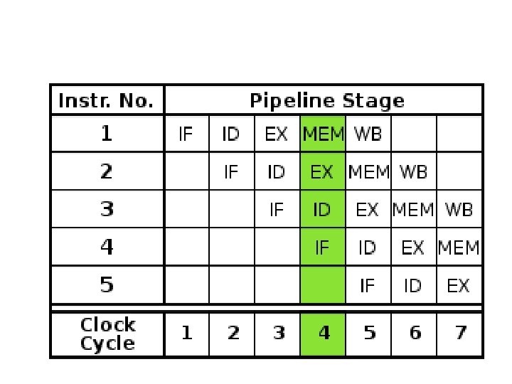
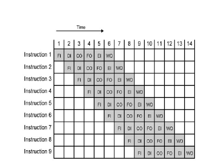
Instruction pipelining • Instruction pipelining is a technique that implements a form of parallelism called instruction-level parallelism within a single processor. • It therefore allows faster CPU throughput (the number of instructions that can be executed in a unit of time). • The basic instruction cycle is broken up into a series called a pipeline. • Rather than processing each instruction sequentially (finishing one instruction before starting the next), each instruction is split up into a sequence of steps so different steps can be executed in parallel and instructions can be processed concurrently
Scalar vs Superscalar