ECE 313 Computer Organization MultiCycle Processor Design 1
![Review: Register Transfers } Instruction Fetch Instruction <- MEM[PC]; } Instruction Execution PC = Review: Register Transfers } Instruction Fetch Instruction <- MEM[PC]; } Instruction Execution PC =](https://slidetodoc.com/presentation_image_h2/f6eb54de397dbdbfa42f2c22b4cfed76/image-8.jpg)
![Multicycle Execution Step (1) Instruction Fetch IR = Memory[PC]; PC = PC + 4; Multicycle Execution Step (1) Instruction Fetch IR = Memory[PC]; PC = PC + 4;](https://slidetodoc.com/presentation_image_h2/f6eb54de397dbdbfa42f2c22b4cfed76/image-11.jpg)
![Multicycle Execution Step (2) Instruction Decode and Register Fetch A = Reg[IR[25 -21]]; (A Multicycle Execution Step (2) Instruction Decode and Register Fetch A = Reg[IR[25 -21]]; (A](https://slidetodoc.com/presentation_image_h2/f6eb54de397dbdbfa42f2c22b4cfed76/image-12.jpg)
![Multicycle Execution Steps (3) Memory Reference Instructions ALUOut = A + sign-extend(IR[15 -0]); Reg[rs] Multicycle Execution Steps (3) Memory Reference Instructions ALUOut = A + sign-extend(IR[15 -0]); Reg[rs]](https://slidetodoc.com/presentation_image_h2/f6eb54de397dbdbfa42f2c22b4cfed76/image-13.jpg)
![Multicycle Execution Steps (3) ALU Instruction (R-Type) ALUOut = A op B Reg[rs] R-Type Multicycle Execution Steps (3) ALU Instruction (R-Type) ALUOut = A op B Reg[rs] R-Type](https://slidetodoc.com/presentation_image_h2/f6eb54de397dbdbfa42f2c22b4cfed76/image-14.jpg)
![Multicycle Execution Steps (3) Branch Instructions if (A == B) PC = ALUOut; Reg[rs] Multicycle Execution Steps (3) Branch Instructions if (A == B) PC = ALUOut; Reg[rs]](https://slidetodoc.com/presentation_image_h2/f6eb54de397dbdbfa42f2c22b4cfed76/image-15.jpg)
![Multicycle Execution Step (3) Jump Instruction PC = PC[31 -28] concat (IR[25 -0] << Multicycle Execution Step (3) Jump Instruction PC = PC[31 -28] concat (IR[25 -0] <<](https://slidetodoc.com/presentation_image_h2/f6eb54de397dbdbfa42f2c22b4cfed76/image-16.jpg)
![Multicycle Execution Steps (4) Memory Access - Read (lw) MDR = Memory[ALUOut]; Reg[rs] Mem. Multicycle Execution Steps (4) Memory Access - Read (lw) MDR = Memory[ALUOut]; Reg[rs] Mem.](https://slidetodoc.com/presentation_image_h2/f6eb54de397dbdbfa42f2c22b4cfed76/image-17.jpg)
![Multicycle Execution Steps (4) Memory Access - Write (sw) Memory[ALUOut] = B; Reg[rs] PC Multicycle Execution Steps (4) Memory Access - Write (sw) Memory[ALUOut] = B; Reg[rs] PC](https://slidetodoc.com/presentation_image_h2/f6eb54de397dbdbfa42f2c22b4cfed76/image-18.jpg)
![Multicycle Execution Steps (4) ALU Instruction (R-Type) Reg[IR[15: 11]] = ALUOUT Reg[rs] R-Type Result Multicycle Execution Steps (4) ALU Instruction (R-Type) Reg[IR[15: 11]] = ALUOUT Reg[rs] R-Type Result](https://slidetodoc.com/presentation_image_h2/f6eb54de397dbdbfa42f2c22b4cfed76/image-19.jpg)
![Multicycle Execution Steps (5) Memory Read Completion (lw) Reg[IR[20 -16]] = MDR; Reg[rs] Mem. Multicycle Execution Steps (5) Memory Read Completion (lw) Reg[IR[20 -16]] = MDR; Reg[rs] Mem.](https://slidetodoc.com/presentation_image_h2/f6eb54de397dbdbfa42f2c22b4cfed76/image-20.jpg)
![Multicycle Execution Step (1) Fetch IR = Memory[PC]; PC = PC + 4; I Multicycle Execution Step (1) Fetch IR = Memory[PC]; PC = PC + 4; I](https://slidetodoc.com/presentation_image_h2/f6eb54de397dbdbfa42f2c22b4cfed76/image-26.jpg)
![Multicycle Execution Step (2) Instruction Decode and Register Fetch A = Reg[IR[25 -21]]; (A Multicycle Execution Step (2) Instruction Decode and Register Fetch A = Reg[IR[25 -21]]; (A](https://slidetodoc.com/presentation_image_h2/f6eb54de397dbdbfa42f2c22b4cfed76/image-27.jpg)
![Multicycle Execution Steps (3) Memory Reference Instructions ALUOut = A + sign-extend(IR[15 -0]); 0 Multicycle Execution Steps (3) Memory Reference Instructions ALUOut = A + sign-extend(IR[15 -0]); 0](https://slidetodoc.com/presentation_image_h2/f6eb54de397dbdbfa42f2c22b4cfed76/image-28.jpg)
![Multicycle Execution Step (3) Jump Instruction PC = PC[21 -28] concat (IR[25 -0] << Multicycle Execution Step (3) Jump Instruction PC = PC[21 -28] concat (IR[25 -0] <<](https://slidetodoc.com/presentation_image_h2/f6eb54de397dbdbfa42f2c22b4cfed76/image-31.jpg)
![Multicycle Execution Steps (4) Memory Access - Read (lw) MDR = Memory[ALUOut]; 0 0 Multicycle Execution Steps (4) Memory Access - Read (lw) MDR = Memory[ALUOut]; 0 0](https://slidetodoc.com/presentation_image_h2/f6eb54de397dbdbfa42f2c22b4cfed76/image-32.jpg)
![Multicycle Execution Steps (4) Memory Access - Write (sw) Memory[ALUOut] = B; 0 0 Multicycle Execution Steps (4) Memory Access - Write (sw) Memory[ALUOut] = B; 0 0](https://slidetodoc.com/presentation_image_h2/f6eb54de397dbdbfa42f2c22b4cfed76/image-33.jpg)
![Multicycle Execution Step (4) ALU Instruction (R-Type) Reg[IR[15: 11]] = ALUOut; 0 (Reg[Rd] = Multicycle Execution Step (4) ALU Instruction (R-Type) Reg[IR[15: 11]] = ALUOut; 0 (Reg[Rd] =](https://slidetodoc.com/presentation_image_h2/f6eb54de397dbdbfa42f2c22b4cfed76/image-34.jpg)
![Multicycle Execution Steps (5) Memory Read Completion (lw) Reg[IR[20 -16]] = MDR; 0 0 Multicycle Execution Steps (5) Memory Read Completion (lw) Reg[IR[20 -16]] = MDR; 0 0](https://slidetodoc.com/presentation_image_h2/f6eb54de397dbdbfa42f2c22b4cfed76/image-35.jpg)
- Slides: 52

ECE 313 - Computer Organization Multi-Cycle Processor Design 1 Feb 2005 Reading: 5. 5 Prof. John Nestor ECE Department Lafayette College Easton, Pennsylvania 18042 nestorj@lafayette. edu Portions of these slides are derived from: Textbook figures © 1998 Morgan Kaufmann Publishers all rights reserved Tod Amon's COD 2 e Slides © 1998 Morgan Kaufmann Publishers all rights reserved Dave Patterson’s CS 152 Slides - Fall 1997 © UCB Rob Rutenbar’s 18 -347 Slides - Fall 1999 CMU Feb 2005 Multicycle Design 1 other sources as noted 1

Outline - Multicycle Design } } } Overview Datapath Design Controller Design Microprogramming Exceptions Performance Considerations Feb 2005 Multicycle Design 1 2

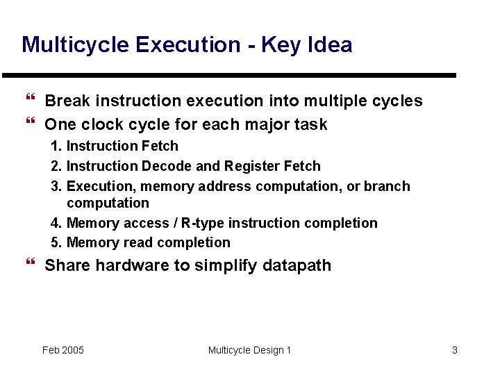
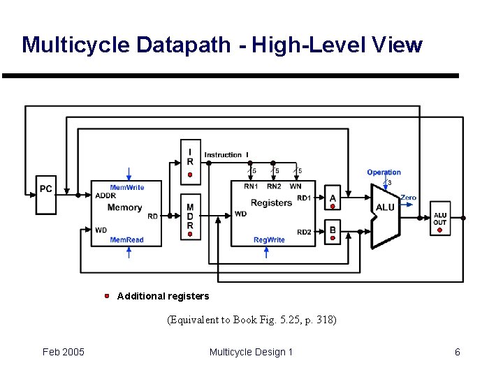
Multicycle Execution - Key Idea } Break instruction execution into multiple cycles } One clock cycle for each major task 1. Instruction Fetch 2. Instruction Decode and Register Fetch 3. Execution, memory address computation, or branch computation 4. Memory access / R-type instruction completion 5. Memory read completion } Share hardware to simplify datapath Feb 2005 Multicycle Design 1 3

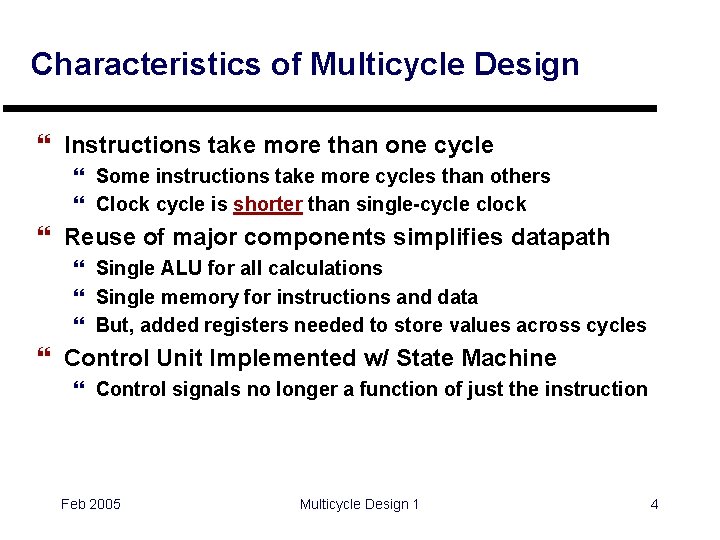
Characteristics of Multicycle Design } Instructions take more than one cycle } Some instructions take more cycles than others } Clock cycle is shorter than single-cycle clock } Reuse of major components simplifies datapath } Single ALU for all calculations } Single memory for instructions and data } But, added registers needed to store values across cycles } Control Unit Implemented w/ State Machine } Control signals no longer a function of just the instruction Feb 2005 Multicycle Design 1 4

Outline - Multicycle Design } } } Overview Datapath Design Controller Design Microprogramming Exceptions Performance Considerations Feb 2005 Multicycle Design 1 5

Multicycle Datapath - High-Level View Additional registers (Equivalent to Book Fig. 5. 25, p. 318) Feb 2005 Multicycle Design 1 6

Review: Steps in Processor Design 1. Analyze instruction set; get datapath requirements 2. Select datapath components and establish clocking methodology 3. Assemble datapath that meets requirements 4. Determine control signal values for each instruction 5. Assemble control logic to generate control signals Feb 2005 Multicycle Design 1 7
![Review Register Transfers Instruction Fetch Instruction MEMPC Instruction Execution PC Review: Register Transfers } Instruction Fetch Instruction <- MEM[PC]; } Instruction Execution PC =](https://slidetodoc.com/presentation_image_h2/f6eb54de397dbdbfa42f2c22b4cfed76/image-8.jpg)
Review: Register Transfers } Instruction Fetch Instruction <- MEM[PC]; } Instruction Execution PC = PC + 4; Key idea: break into multiple cycles! Instr. Register Transfers add sub and or lw sw beq R[rd] <- R[rs] + R[rt]; R[rd] <- R[rs] - R[rt]; R[rd] <- R[rs] & R[rt]; R[rd] <- R[rs] | R[rt]; R[rt] <- MEM[R[rs] + s_extend(offset)]; MEM[R[rs] + sign_extend(offset)] <- R[rt]; PC <- PC + 4 if (R[rs] == R[rt]) then PC <- PC+4 + s_extend(offset<<2) j else PC <- PC + 4 PC <- upper(PC)@(address << 2) Feb 2005 Multicycle Design 1 8

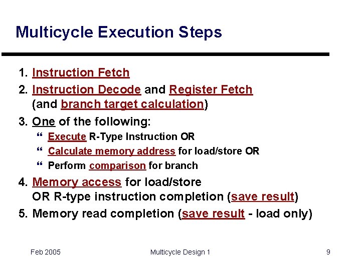
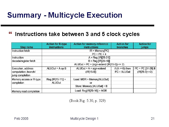
Multicycle Execution Steps 1. Instruction Fetch 2. Instruction Decode and Register Fetch (and branch target calculation) 3. One of the following: } Execute R-Type Instruction OR } Calculate memory address for load/store OR } Perform comparison for branch 4. Memory access for load/store OR R-type instruction completion (save result) 5. Memory read completion (save result - load only) Feb 2005 Multicycle Design 1 9

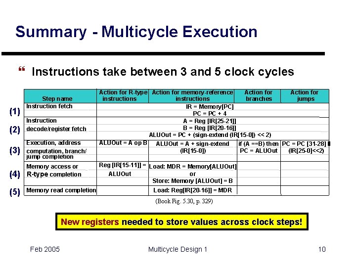
Summary - Multicycle Execution } Instructions take between 3 and 5 clock cycles (1) (2) (3) (4) (5) Step name Instruction fetch Instruction decode/register fetch Execution, address computation, branch/ jump completion Memory access or R-type completion Memory read completion Action for R-type Action for memory-reference instructions branches jumps IR = Memory[PC] PC = PC + 4 A = Reg [IR[25 -21]] B = Reg [IR[20 -16]] ALUOut = PC + (sign-extend (IR[15 -0]) << 2) ALUOut = A op B ALUOut = A + sign-extend if (A ==B) then PC = PC [31 -28] II (IR[15 -0]) PC = ALUOut (IR[25 -0]<<2) Reg [IR[15 -11]] = Load: MDR = Memory[ALUOut] ALUOut or Store: Memory [ALUOut] = B Load: Reg[IR[20 -16]] = MDR (Book Fig. 5. 30, p. 329) New registers needed to store values across clock steps! Feb 2005 Multicycle Design 1 10
![Multicycle Execution Step 1 Instruction Fetch IR MemoryPC PC PC 4 Multicycle Execution Step (1) Instruction Fetch IR = Memory[PC]; PC = PC + 4;](https://slidetodoc.com/presentation_image_h2/f6eb54de397dbdbfa42f2c22b4cfed76/image-11.jpg)
Multicycle Execution Step (1) Instruction Fetch IR = Memory[PC]; PC = PC + 4; 4 PC + 4 Feb 2005 Multicycle Design 1 11
![Multicycle Execution Step 2 Instruction Decode and Register Fetch A RegIR25 21 A Multicycle Execution Step (2) Instruction Decode and Register Fetch A = Reg[IR[25 -21]]; (A](https://slidetodoc.com/presentation_image_h2/f6eb54de397dbdbfa42f2c22b4cfed76/image-12.jpg)
Multicycle Execution Step (2) Instruction Decode and Register Fetch A = Reg[IR[25 -21]]; (A = Reg[rs]) B = Reg[IR[20 -15]]; (B = Reg[rt]) ALUOut = (PC + sign-extend(IR[15 -0]) << 2) Reg[rs] Branch Target Address PC + 4 Reg[rt] Feb 2005 Multicycle Design 1 12
![Multicycle Execution Steps 3 Memory Reference Instructions ALUOut A signextendIR15 0 Regrs Multicycle Execution Steps (3) Memory Reference Instructions ALUOut = A + sign-extend(IR[15 -0]); Reg[rs]](https://slidetodoc.com/presentation_image_h2/f6eb54de397dbdbfa42f2c22b4cfed76/image-13.jpg)
Multicycle Execution Steps (3) Memory Reference Instructions ALUOut = A + sign-extend(IR[15 -0]); Reg[rs] Mem. Address PC + 4 Reg[rt] Feb 2005 Multicycle Design 1 13
![Multicycle Execution Steps 3 ALU Instruction RType ALUOut A op B Regrs RType Multicycle Execution Steps (3) ALU Instruction (R-Type) ALUOut = A op B Reg[rs] R-Type](https://slidetodoc.com/presentation_image_h2/f6eb54de397dbdbfa42f2c22b4cfed76/image-14.jpg)
Multicycle Execution Steps (3) ALU Instruction (R-Type) ALUOut = A op B Reg[rs] R-Type Result PC + 4 Reg[rt] Feb 2005 Multicycle Design 1 14
![Multicycle Execution Steps 3 Branch Instructions if A B PC ALUOut Regrs Multicycle Execution Steps (3) Branch Instructions if (A == B) PC = ALUOut; Reg[rs]](https://slidetodoc.com/presentation_image_h2/f6eb54de397dbdbfa42f2c22b4cfed76/image-15.jpg)
Multicycle Execution Steps (3) Branch Instructions if (A == B) PC = ALUOut; Reg[rs] Branch Target Address Feb 2005 Branch Target Address Reg[rt] Multicycle Design 1 15
![Multicycle Execution Step 3 Jump Instruction PC PC31 28 concat IR25 0 Multicycle Execution Step (3) Jump Instruction PC = PC[31 -28] concat (IR[25 -0] <<](https://slidetodoc.com/presentation_image_h2/f6eb54de397dbdbfa42f2c22b4cfed76/image-16.jpg)
Multicycle Execution Step (3) Jump Instruction PC = PC[31 -28] concat (IR[25 -0] << 2) Reg[rs] Branch Target Address Jump Address Reg[rt] Feb 2005 Multicycle Design 1 16
![Multicycle Execution Steps 4 Memory Access Read lw MDR MemoryALUOut Regrs Mem Multicycle Execution Steps (4) Memory Access - Read (lw) MDR = Memory[ALUOut]; Reg[rs] Mem.](https://slidetodoc.com/presentation_image_h2/f6eb54de397dbdbfa42f2c22b4cfed76/image-17.jpg)
Multicycle Execution Steps (4) Memory Access - Read (lw) MDR = Memory[ALUOut]; Reg[rs] Mem. Address PC + 4 Mem. Data Feb 2005 Reg[rt] Multicycle Design 1 17
![Multicycle Execution Steps 4 Memory Access Write sw MemoryALUOut B Regrs PC Multicycle Execution Steps (4) Memory Access - Write (sw) Memory[ALUOut] = B; Reg[rs] PC](https://slidetodoc.com/presentation_image_h2/f6eb54de397dbdbfa42f2c22b4cfed76/image-18.jpg)
Multicycle Execution Steps (4) Memory Access - Write (sw) Memory[ALUOut] = B; Reg[rs] PC + 4 Reg[rt] Feb 2005 Multicycle Design 1 18
![Multicycle Execution Steps 4 ALU Instruction RType RegIR15 11 ALUOUT Regrs RType Result Multicycle Execution Steps (4) ALU Instruction (R-Type) Reg[IR[15: 11]] = ALUOUT Reg[rs] R-Type Result](https://slidetodoc.com/presentation_image_h2/f6eb54de397dbdbfa42f2c22b4cfed76/image-19.jpg)
Multicycle Execution Steps (4) ALU Instruction (R-Type) Reg[IR[15: 11]] = ALUOUT Reg[rs] R-Type Result PC + 4 Reg[rt] Feb 2005 Multicycle Design 1 19
![Multicycle Execution Steps 5 Memory Read Completion lw RegIR20 16 MDR Regrs Mem Multicycle Execution Steps (5) Memory Read Completion (lw) Reg[IR[20 -16]] = MDR; Reg[rs] Mem.](https://slidetodoc.com/presentation_image_h2/f6eb54de397dbdbfa42f2c22b4cfed76/image-20.jpg)
Multicycle Execution Steps (5) Memory Read Completion (lw) Reg[IR[20 -16]] = MDR; Reg[rs] Mem. Address PC + 4 Mem. Data Feb 2005 Reg[rt] Multicycle Design 1 20

Summary - Multicycle Execution } Instructions take between 3 and 5 clock cycles (Book Fig. 5. 30, p. 329) Feb 2005 Multicycle Design 1 21

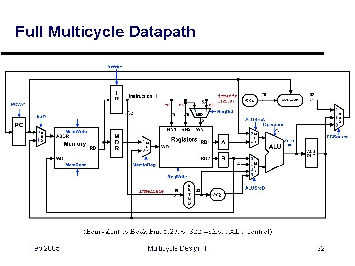
Full Multicycle Datapath (Equivalent to Book Fig. 5. 27, p. 322 without ALU control) Feb 2005 Multicycle Design 1 22

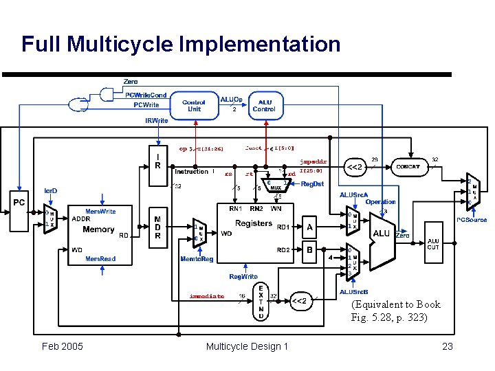
Full Multicycle Implementation (Equivalent to Book Fig. 5. 28, p. 323) Feb 2005 Multicycle Design 1 23

Outline - Multicycle Design } } } Overview Datapath Design Controller Design Performance Considerations Microprogramming Exceptions Feb 2005 Multicycle Design 1 24

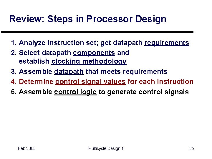
Review: Steps in Processor Design 1. Analyze instruction set; get datapath requirements 2. Select datapath components and establish clocking methodology 3. Assemble datapath that meets requirements 4. Determine control signal values for each instruction 5. Assemble control logic to generate control signals Feb 2005 Multicycle Design 1 25
![Multicycle Execution Step 1 Fetch IR MemoryPC PC PC 4 I Multicycle Execution Step (1) Fetch IR = Memory[PC]; PC = PC + 4; I](https://slidetodoc.com/presentation_image_h2/f6eb54de397dbdbfa42f2c22b4cfed76/image-26.jpg)
Multicycle Execution Step (1) Fetch IR = Memory[PC]; PC = PC + 4; I R 1 PCWr* 1 IRWrite Instruction I jmpaddr rs 0 0 Ior. D 32 5 U 1 X RN 1 Mem. Write ADDR Memory 5 0 MUX RD M D R 1 M U 0 X RN 2 Registers WD RD 1 RD 2 Mem. Read 1 X Reg. Write 0 immediate 16 E X T N D 32 Multicycle Design 1 2 010 U 1 X 4 0 1 M U 2 X 3 0 X 3 PCSource Zero ALU 0 ALU OUT ALUSrc. B <<2 M 1 U Operation A B 32 CONCAT 0 M Memto. Reg X 28 <<2 0 ALUSrc. A Reg. Dst WN WD Feb 2005 rd 1 5 PC 0 M 5 rt I[25: 0] 1 26
![Multicycle Execution Step 2 Instruction Decode and Register Fetch A RegIR25 21 A Multicycle Execution Step (2) Instruction Decode and Register Fetch A = Reg[IR[25 -21]]; (A](https://slidetodoc.com/presentation_image_h2/f6eb54de397dbdbfa42f2c22b4cfed76/image-27.jpg)
Multicycle Execution Step (2) Instruction Decode and Register Fetch A = Reg[IR[25 -21]]; (A = Reg[rs]) B = Reg[IR[20 -15]]; (B = Reg[rt]) ALUOut = (PC + sign-extend(IR[15 -0]) << 2) 0 0 X 0 010 X 0 3 Feb 2005 Multicycle Design 1 27
![Multicycle Execution Steps 3 Memory Reference Instructions ALUOut A signextendIR15 0 0 Multicycle Execution Steps (3) Memory Reference Instructions ALUOut = A + sign-extend(IR[15 -0]); 0](https://slidetodoc.com/presentation_image_h2/f6eb54de397dbdbfa42f2c22b4cfed76/image-28.jpg)
Multicycle Execution Steps (3) Memory Reference Instructions ALUOut = A + sign-extend(IR[15 -0]); 0 0 X 1 010 X 0 2 Feb 2005 Multicycle Design 1 28

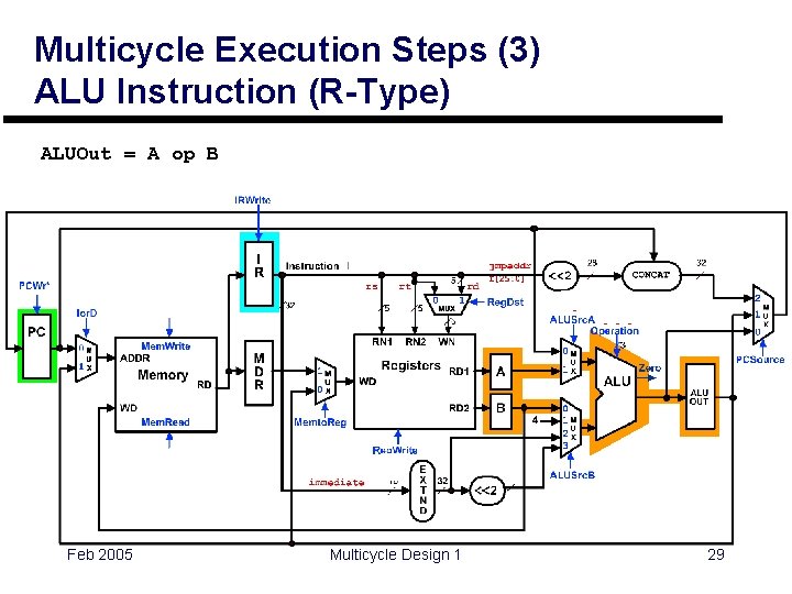
Multicycle Execution Steps (3) ALU Instruction (R-Type) ALUOut = A op B 0 0 X 1 ? ? ? X 0 0 Feb 2005 Multicycle Design 1 29

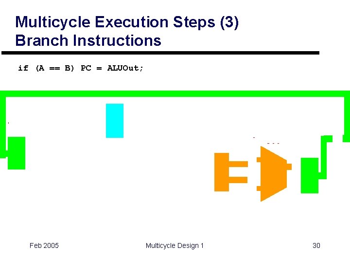
Multicycle Execution Steps (3) Branch Instructions if (A == B) PC = ALUOut; 0 1 if Zero=1 X 0 X 1 011 1 0 X 0 0 Feb 2005 Multicycle Design 1 30
![Multicycle Execution Step 3 Jump Instruction PC PC21 28 concat IR25 0 Multicycle Execution Step (3) Jump Instruction PC = PC[21 -28] concat (IR[25 -0] <<](https://slidetodoc.com/presentation_image_h2/f6eb54de397dbdbfa42f2c22b4cfed76/image-31.jpg)
Multicycle Execution Step (3) Jump Instruction PC = PC[21 -28] concat (IR[25 -0] << 2) 0 1 X 0 X X XXX 2 0 X Feb 2005 Multicycle Design 1 31
![Multicycle Execution Steps 4 Memory Access Read lw MDR MemoryALUOut 0 0 Multicycle Execution Steps (4) Memory Access - Read (lw) MDR = Memory[ALUOut]; 0 0](https://slidetodoc.com/presentation_image_h2/f6eb54de397dbdbfa42f2c22b4cfed76/image-32.jpg)
Multicycle Execution Steps (4) Memory Access - Read (lw) MDR = Memory[ALUOut]; 0 0 1 0 X X XXX X 1 X 0 X Feb 2005 Multicycle Design 1 32
![Multicycle Execution Steps 4 Memory Access Write sw MemoryALUOut B 0 0 Multicycle Execution Steps (4) Memory Access - Write (sw) Memory[ALUOut] = B; 0 0](https://slidetodoc.com/presentation_image_h2/f6eb54de397dbdbfa42f2c22b4cfed76/image-33.jpg)
Multicycle Execution Steps (4) Memory Access - Write (sw) Memory[ALUOut] = B; 0 0 1 1 X X XXX X 0 X Feb 2005 Multicycle Design 1 33
![Multicycle Execution Step 4 ALU Instruction RType RegIR15 11 ALUOut 0 RegRd Multicycle Execution Step (4) ALU Instruction (R-Type) Reg[IR[15: 11]] = ALUOut; 0 (Reg[Rd] =](https://slidetodoc.com/presentation_image_h2/f6eb54de397dbdbfa42f2c22b4cfed76/image-34.jpg)
Multicycle Execution Step (4) ALU Instruction (R-Type) Reg[IR[15: 11]] = ALUOut; 0 (Reg[Rd] = ALUOut) 0 X 0 1 X XXX X 0 1 1 X Feb 2005 Multicycle Design 1 34
![Multicycle Execution Steps 5 Memory Read Completion lw RegIR20 16 MDR 0 0 Multicycle Execution Steps (5) Memory Read Completion (lw) Reg[IR[20 -16]] = MDR; 0 0](https://slidetodoc.com/presentation_image_h2/f6eb54de397dbdbfa42f2c22b4cfed76/image-35.jpg)
Multicycle Execution Steps (5) Memory Read Completion (lw) Reg[IR[20 -16]] = MDR; 0 0 X XXX X 0 Feb 2005 10 1 Multicycle Design 1 X 35

Review: Steps in Processor Design 1. Analyze instruction set; get datapath requirements 2. Select datapath components and establish clocking methodology 3. Assemble datapath that meets requirements 4. Determine control signal values for each instruction 5. Assemble control logic to generate control signals Feb 2005 Multicycle Design 1 36

Full Multicycle Implementation Feb 2005 Multicycle Design 1 37

Multicycle Control Unit } Review: single-cycle implementation } All control signals can be determined by current instruction + condition } Implemented in combinational logic } Multicycle implementation is different } Control signals depend on • current instruction • which clock cycle is currently being executed } Implemented as • Finite State Machine (FSM) OR • Microprogrammed Implementation - “stylized FSM” Feb 2005 Multicycle Design 1 38

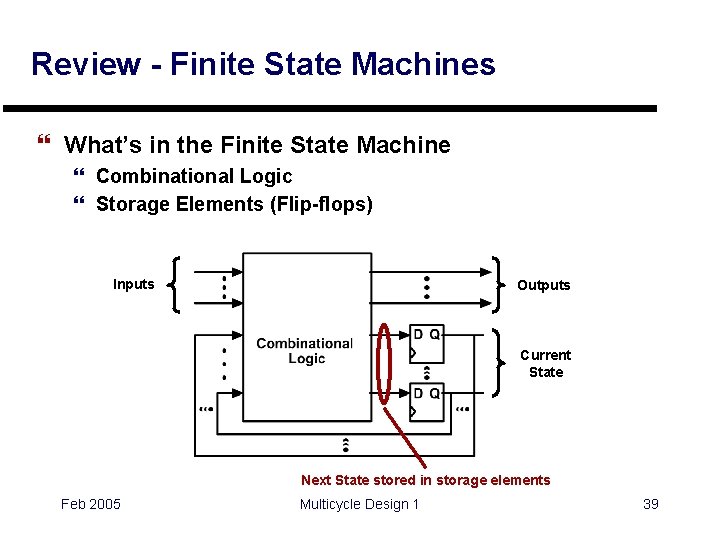
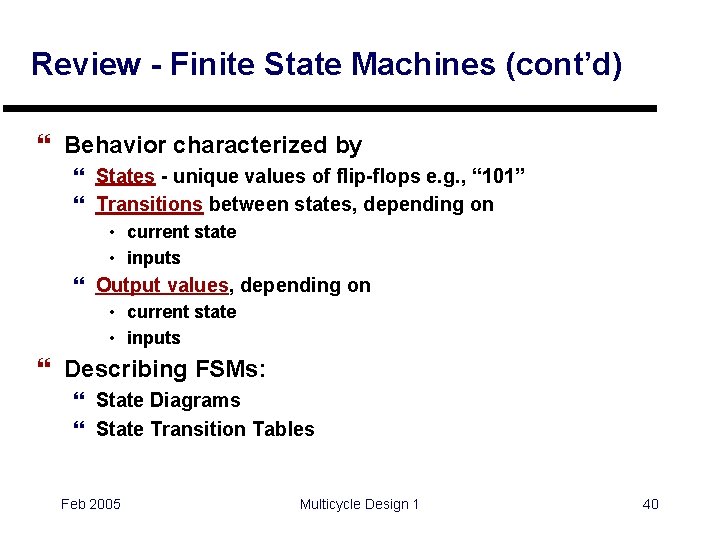
Review - Finite State Machines } What’s in the Finite State Machine } Combinational Logic } Storage Elements (Flip-flops) Inputs Outputs Current State Next State stored in storage elements Feb 2005 Multicycle Design 1 39

Review - Finite State Machines (cont’d) } Behavior characterized by } States - unique values of flip-flops e. g. , “ 101” } Transitions between states, depending on • current state • inputs } Output values, depending on • current state • inputs } Describing FSMs: } State Diagrams } State Transition Tables Feb 2005 Multicycle Design 1 40

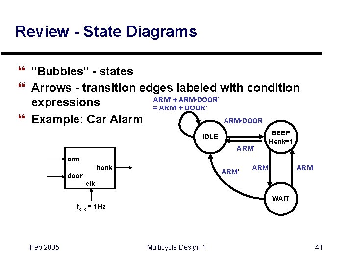
Review - State Diagrams } "Bubbles" - states } Arrows - transition edges labeled with condition ARM’ + ARM • DOOR’ expressions = ARM’ + DOOR’ } Example: Car Alarm ARM • DOOR IDLE ARM’ BEEP Honk=1 arm honk ARM’ door ARM clk WAIT fclk = 1 Hz Feb 2005 Multicycle Design 1 41

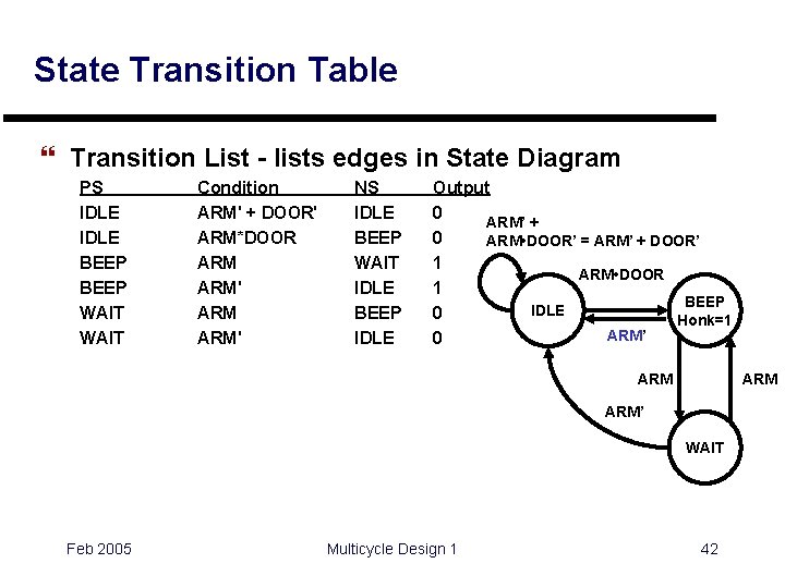
State Transition Table } Transition List - lists edges in State Diagram PS IDLE BEEP WAIT Condition ARM' + DOOR' ARM*DOOR ARM ARM' NS IDLE BEEP WAIT IDLE BEEP IDLE Output 0 ARM’ + 0 ARM • DOOR’ = ARM’ + DOOR’ 1 ARM • DOOR 1 BEEP IDLE 0 Honk=1 ARM’ 0 ARM ARM’ WAIT Feb 2005 Multicycle Design 1 42

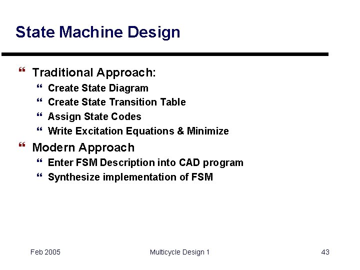
State Machine Design } Traditional Approach: } } Create State Diagram Create State Transition Table Assign State Codes Write Excitation Equations & Minimize } Modern Approach } Enter FSM Description into CAD program } Synthesize implementation of FSM Feb 2005 Multicycle Design 1 43

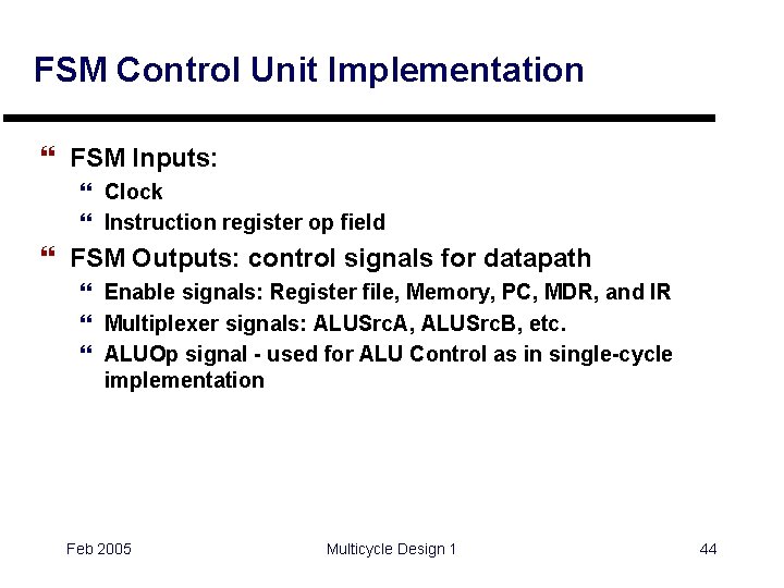
FSM Control Unit Implementation } FSM Inputs: } Clock } Instruction register op field } FSM Outputs: control signals for datapath } Enable signals: Register file, Memory, PC, MDR, and IR } Multiplexer signals: ALUSrc. A, ALUSrc. B, etc. } ALUOp signal - used for ALU Control as in single-cycle implementation Feb 2005 Multicycle Design 1 44

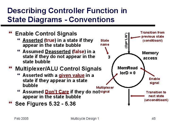
} Enable Control Signals } Asserted (true) in a state if they appear in the state bubble } Assumed Deasserted (false) in a state if they do not appear in the state bubble State name } Asserted with a given value in a state if they appear in a state bubble Multiplexer } Assumed Don’t Care if they do not signal appear in the state bubble Feb 2005 Multicycle Design 1 Transition from previous state (conditioanl) Memory access 3 } Multiplexer/ALU Control Signals } See Figures 5. 32 - 5. 36 (Op=‘LW’) Describing Controller Function in State Diagrams - Conventions Mem. Read Ior. D = 0 Enable signal Transition to next state (unconditioanl) 45

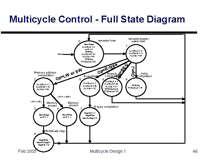
Multicycle Control - Full State Diagram Mem. Read ALUSrc. A = 0 Ior. D = 0 IRWrite ALUSrc. B = 01 ALUOp = 00 PCWrite PCSource = 00 6 Execution ALUSrc. A = 1 ALUSrc. B = 00 ALUOp = 10 ALUSrc. A = 1 ALUSrc. B = 10 ALUOp = 00 Op 8 pe y R-t Branch Completion ALUSrc. A = 1 ALUSrc. B = 00 ALUOp = 01 PCWrite. Cond PCSource = 01 9 Op=J = W or S ALUSrc. A = 0 ALUSrc. B = 11 ALUOp = 00 =B EQ Memory address computation LW 2 Op= 1 Op Start Instruction decode / register fetch Instruction Fetch 0 Jump Completion PCWrite PCSource = 10 (OP = (‘SW’) (OP =‘LW’) 3 Mem. Read Ior. D = 1 4 Memory access 5 7 Mem. Write Ior. D = 1 R-type completion Reg. Dst = 1 Reg. Write Memto. Reg = 0 Writeback step Reg. Write Mem. To. Reg=1 Reg. Dst = 0 Feb 2005 Multicycle Design 1 46

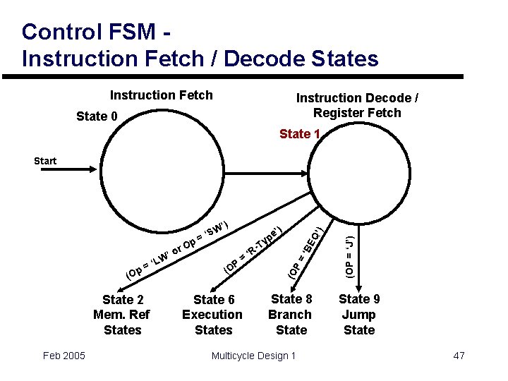
Control FSM Instruction Fetch / Decode States Instruction Fetch State 1 ALUSrc. A = 0 ALUSrc. B = 11 ALUOp = 00 ‘ p= (O State 2 Mem. Ref States Feb 2005 ) EQ ’ Op - P (O = State 6 Execution States ‘R ‘B LW r ’o ’) pe y T State 8 Branch State Multicycle Design 1 (OP = ‘J’) ’) SW =‘ P= Start Mem. Read ALUSrc. A = 0 Ior. D = 0 IRWrite ALUSrc. B = 01 ALUOp = 00 PCWrite PCSource = 00 (O State 0 Instruction Decode / Register Fetch State 9 Jump State 47

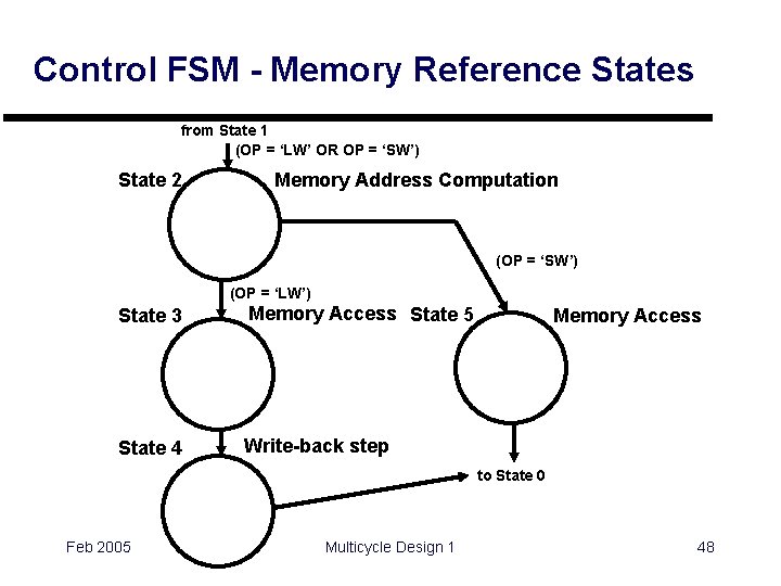
Control FSM - Memory Reference States from State 1 (OP = ‘LW’ OR OP = ‘SW’) State 2 Memory Address Computation ALUSrc. A = 1 ALUSrc. B = 10 ALUOp = 00 (OP = ‘SW’) (OP = ‘LW’) State 3 Memory Access State 5 Mem. Write Ior. D = 1 Mem. Read Ior. D = 1 State 4 Write-back step to State 0 Reg. Write Mem. To. Reg=1 Reg. Dst = 0 Feb 2005 Memory Access Multicycle Design 1 48

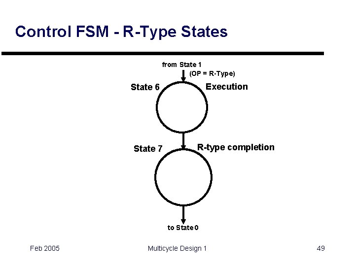
Control FSM - R-Type States from State 1 (OP = R-Type) Execution State 6 ALUSrc. A = 1 ALUSrc. B = 00 ALUOp = 10 State 7 R-type completion Reg. Dst = 1 Reg. Write Memto. Reg = 0 to State 0 Feb 2005 Multicycle Design 1 49

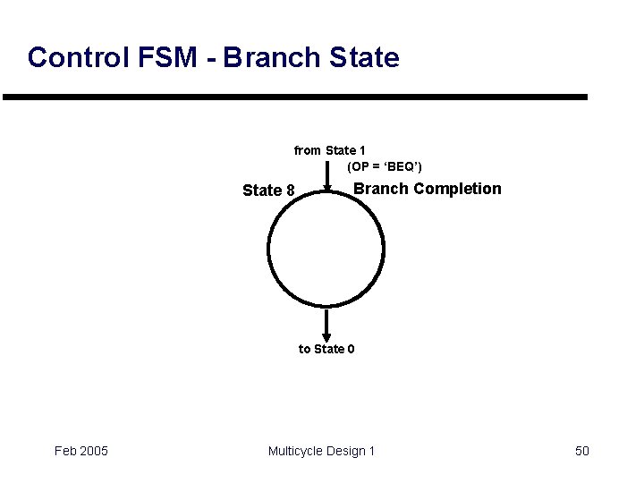
Control FSM - Branch State from State 1 (OP = ‘BEQ’) State 8 Branch Completion ALUSrc. A = 1 ALUSrc. B = 00 ALUOp = 01 PCWrite. Cond PCSource = 01 to State 0 Feb 2005 Multicycle Design 1 50

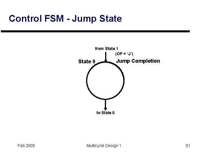
Control FSM - Jump State from State 1 (OP = ‘J’) Jump Completion State 9 PCWrite PCSource = 10 to State 0 Feb 2005 Multicycle Design 1 51

Coming Up } } Multicycle Implementation Performance Multicycle Controller Implementation Microprogrammed Control Exceptions Feb 2005 Multicycle Design 1 52