CPU Design CPU Design Flow TsungChu Huang Dept


![reg[1]+reg[2] ALU Data memory 2 reg[1] imm add r 3, r 1, r 2 reg[1]+reg[2] ALU Data memory 2 reg[1] imm add r 3, r 1, r 2](https://slidetodoc.com/presentation_image_h2/4c660843383a415a675dfc6103344681/image-13.jpg)

![Fetch Note: These 5 stages were there all along! IR <= MEM[PC] PC <= Fetch Note: These 5 stages were there all along! IR <= MEM[PC] PC <=](https://slidetodoc.com/presentation_image_h2/4c660843383a415a675dfc6103344681/image-23.jpg)
![lw r 1 WB Ctrl M[r 2+35] Reg. File add. I r 2 sub lw r 1 WB Ctrl M[r 2+35] Reg. File add. I r 2 sub](https://slidetodoc.com/presentation_image_h2/4c660843383a415a675dfc6103344681/image-79.jpg)
![Reg. File r 1=M[r 2+35] add. I r 2 WB Ctrl r 2+3 sub Reg. File r 1=M[r 2+35] add. I r 2 WB Ctrl r 2+3 sub](https://slidetodoc.com/presentation_image_h2/4c660843383a415a675dfc6103344681/image-80.jpg)

- Slides: 95

CPU Design -- CPU Design Flow Tsung-Chu Huang Dept. of Electronic Eng. National Changhua University of Ed. Email: tch@cc. ncue. edu. tw 2005/03/22 CPU Design T. -C. Huang / NCUE Spring 2005 1

Outline Ø A Simple Example to Illustrate 3 Styles Suspended Ø FSM Style Ø ASM Style Ø Microprogramming Ø Stage Scheduling Ø Fixed (Static) Stages Ø Dynamic Scheduling Ø Pipeline Ø Datapath Ø Pipelined Datapath CPU Design T. -C. Huang / NCUE Spring 2005 2

Rethink Ø Ø Ø CPU Design Can We Teach CPU Design without Case Example? Difficult! Familiar Example or Any Example? How Can We Catch the Case Features Soon? T. -C. Huang / NCUE Spring 2005 3

Typical Stages CPU Design T. -C. Huang / NCUE Spring 2005 4

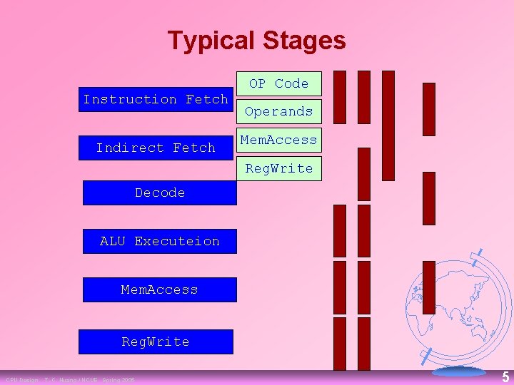
Typical Stages Instruction Fetch Indirect Fetch OP Code Operands Mem. Access Reg. Write Decode ALU Executeion Mem. Access Reg. Write CPU Design T. -C. Huang / NCUE Spring 2005 5

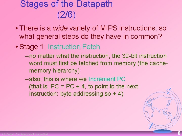
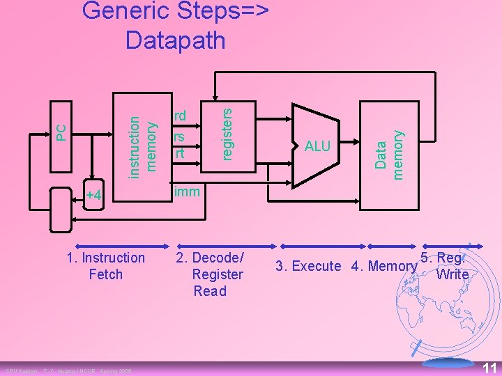
Stages of the Datapath (2/6) • There is a wide variety of MIPS instructions: so what general steps do they have in common? • Stage 1: Instruction Fetch – no matter what the instruction, the 32 bit instruction word must first be fetched from memory (the cache memory hierarchy) – also, this is where we Increment PC (that is, PC = PC + 4, to point to the next instruction: byte addressing so + 4) CPU Design T. -C. Huang / NCUE Spring 2005 6

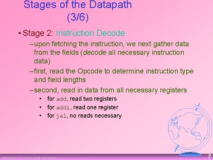
Stages of the Datapath (3/6) • Stage 2: Instruction Decode – upon fetching the instruction, we next gather data from the fields (decode all necessary instruction data) – first, read the Opcode to determine instruction type and field lengths – second, read in data from all necessary registers • for add, read two registers • for addi, read one register • for jal, no reads necessary CPU Design T. -C. Huang / NCUE Spring 2005 7

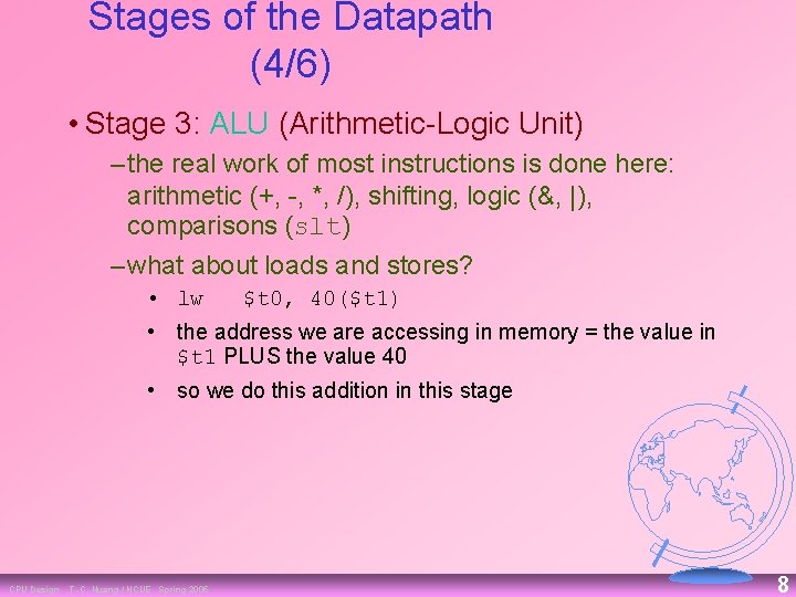
Stages of the Datapath (4/6) • Stage 3: ALU (Arithmetic Logic Unit) – the real work of most instructions is done here: arithmetic (+, , *, /), shifting, logic (&, |), comparisons (slt) – what about loads and stores? • lw $t 0, 40($t 1) • the address we are accessing in memory = the value in $t 1 PLUS the value 40 • so we do this addition in this stage CPU Design T. -C. Huang / NCUE Spring 2005 8

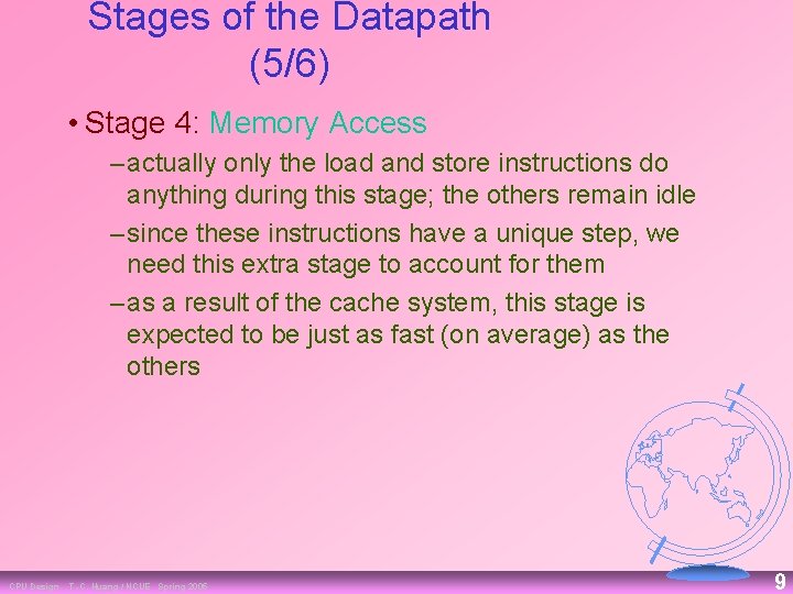
Stages of the Datapath (5/6) • Stage 4: Memory Access – actually only the load and store instructions do anything during this stage; the others remain idle – since these instructions have a unique step, we need this extra stage to account for them – as a result of the cache system, this stage is expected to be just as fast (on average) as the others CPU Design T. -C. Huang / NCUE Spring 2005 9

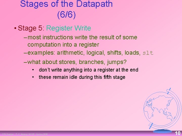
Stages of the Datapath (6/6) • Stage 5: Register Write – most instructions write the result of some computation into a register – examples: arithmetic, logical, shifts, loads, slt – what about stores, branches, jumps? • don’t write anything into a register at the end • these remain idle during this fifth stage CPU Design T. -C. Huang / NCUE Spring 2005 10

+4 1. Instruction Fetch CPU Design T. -C. Huang / NCUE Spring 2005 ALU Data memory rd rs rt registers PC instruction memory Generic Steps=> Datapath imm 2. Decode/ Register Read 3. Execute 4. Memory 5. Reg. Write 11

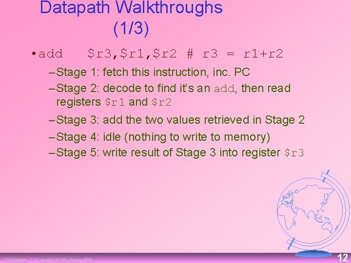
Datapath Walkthroughs (1/3) • add $r 3, $r 1, $r 2 # r 3 = r 1+r 2 – Stage 1: fetch this instruction, inc. PC – Stage 2: decode to find it’s an add, then read registers $r 1 and $r 2 – Stage 3: add the two values retrieved in Stage 2 – Stage 4: idle (nothing to write to memory) – Stage 5: write result of Stage 3 into register $r 3 CPU Design T. -C. Huang / NCUE Spring 2005 12
![reg1reg2 ALU Data memory 2 reg1 imm add r 3 r 1 r 2 reg[1]+reg[2] ALU Data memory 2 reg[1] imm add r 3, r 1, r 2](https://slidetodoc.com/presentation_image_h2/4c660843383a415a675dfc6103344681/image-13.jpg)
reg[1]+reg[2] ALU Data memory 2 reg[1] imm add r 3, r 1, r 2 +4 3 1 registers PC instruction memory Example: ADD Instruction CPU Design T. -C. Huang / NCUE Spring 2005 13

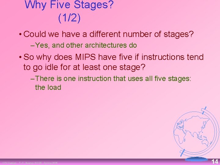
Why Five Stages? (1/2) • Could we have a different number of stages? – Yes, and other architectures do • So why does MIPS have five if instructions tend to go idle for at least one stage? – There is one instruction that uses all five stages: the load CPU Design T. -C. Huang / NCUE Spring 2005 14

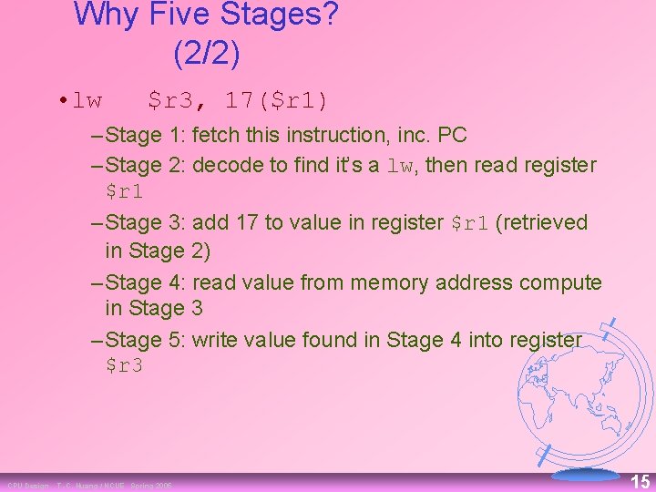
Why Five Stages? (2/2) • lw $r 3, 17($r 1) – Stage 1: fetch this instruction, inc. PC – Stage 2: decode to find it’s a lw, then read register $r 1 – Stage 3: add 17 to value in register $r 1 (retrieved in Stage 2) – Stage 4: read value from memory address compute in Stage 3 – Stage 5: write value found in Stage 4 into register $r 3 CPU Design T. -C. Huang / NCUE Spring 2005 15

Pipeline CPU Design T. -C. Huang / NCUE Spring 2005 16

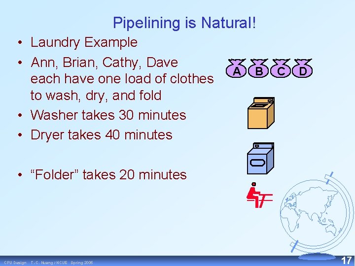
Pipelining is Natural! • Laundry Example • Ann, Brian, Cathy, Dave each have one load of clothes to wash, dry, and fold • Washer takes 30 minutes • Dryer takes 40 minutes A B C D • “Folder” takes 20 minutes CPU Design T. -C. Huang / NCUE Spring 2005 17

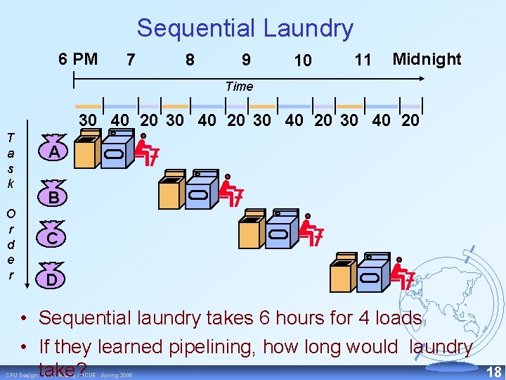
Sequential Laundry 6 PM 7 8 9 10 11 Midnight Time 30 40 20 T a s k A B O r d e r C D • Sequential laundry takes 6 hours for 4 loads • If they learned pipelining, how long would laundry take? CPU Design T. -C. Huang / NCUE Spring 2005 18

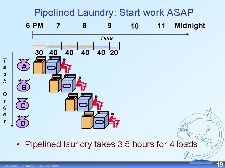
Pipelined Laundry: Start work ASAP 6 PM 7 8 9 10 11 Midnight Time 30 40 T a s k 40 40 40 20 A B O r d e r C D • Pipelined laundry takes 3. 5 hours for 4 loads CPU Design T. -C. Huang / NCUE Spring 2005 19

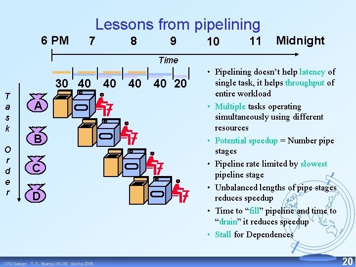
Lessons from pipelining 6 PM 7 8 9 10 11 Midnight Time 30 40 T a s k O r d e r CPU Design A B C D T. -C. Huang / NCUE Spring 2005 40 40 40 20 • Pipelining doesn’t help latency of single task, it helps throughput of entire workload • Multiple tasks operating simultaneously using different resources • Potential speedup = Number pipe stages • Pipeline rate limited by slowest pipeline stage • Unbalanced lengths of pipe stages reduces speedup • Time to “fill” pipeline and time to “drain” it reduces speedup • Stall for Dependences 20

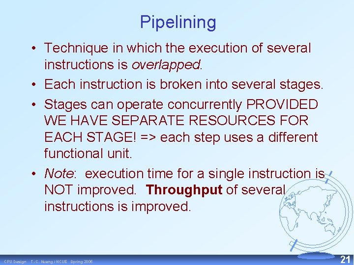
Pipelining • Technique in which the execution of several instructions is overlapped. • Each instruction is broken into several stages. • Stages can operate concurrently PROVIDED WE HAVE SEPARATE RESOURCES FOR EACH STAGE! => each step uses a different functional unit. • Note: execution time for a single instruction is NOT improved. Throughput of several instructions is improved. CPU Design T. -C. Huang / NCUE Spring 2005 21

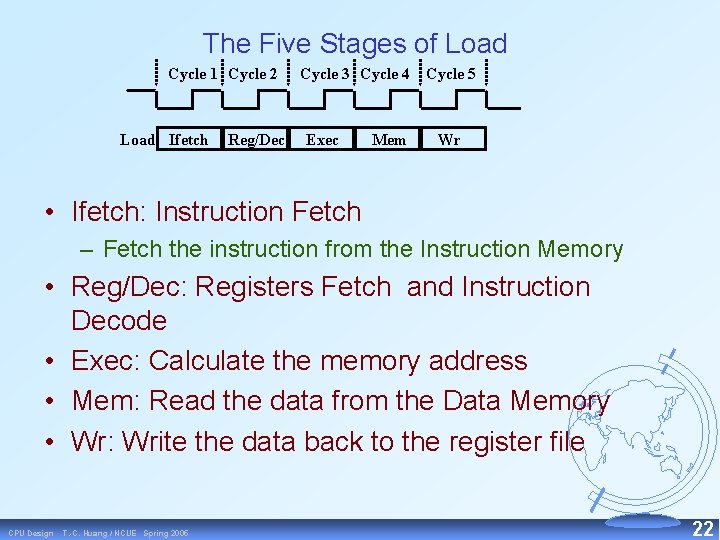
The Five Stages of Load Cycle 1 Cycle 2 Load Ifetch Reg/Dec Cycle 3 Cycle 4 Cycle 5 Exec Mem Wr • Ifetch: Instruction Fetch – Fetch the instruction from the Instruction Memory • Reg/Dec: Registers Fetch and Instruction Decode • Exec: Calculate the memory address • Mem: Read the data from the Data Memory • Wr: Write the data back to the register file CPU Design T. -C. Huang / NCUE Spring 2005 22
![Fetch Note These 5 stages were there all along IR MEMPC PC Fetch Note: These 5 stages were there all along! IR <= MEM[PC] PC <=](https://slidetodoc.com/presentation_image_h2/4c660843383a415a675dfc6103344681/image-23.jpg)
Fetch Note: These 5 stages were there all along! IR <= MEM[PC] PC <= PC + 4 Decode 0000 ALUout <= PC +SX Memory Write-back Execute 0001 CPU Design R type ALUout <= A fun B 0100 ORi ALUout <= A op ZX 0110 LW ALUout <= A + SX 1000 M <= MEM[ALUout] 1001 R[rd] <= ALUout 0101 T. -C. Huang / NCUE Spring 2005 R[rt] <= ALUout 0111 BEQ SW ALUout <= A + SX 1011 If A = B then PC <= ALUout 0010 MEM[ALUout] <= B 1100 R[rt] <= M 1010 23

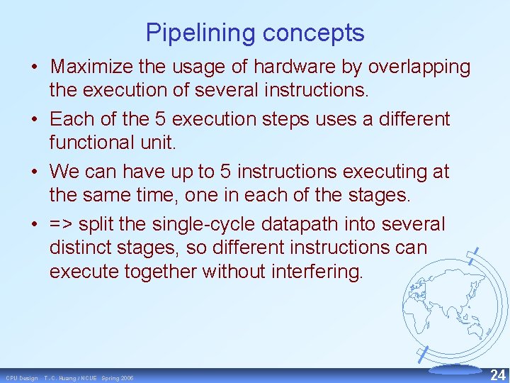
Pipelining concepts • Maximize the usage of hardware by overlapping the execution of several instructions. • Each of the 5 execution steps uses a different functional unit. • We can have up to 5 instructions executing at the same time, one in each of the stages. • => split the single cycle datapath into several distinct stages, so different instructions can execute together without interfering. CPU Design T. -C. Huang / NCUE Spring 2005 24

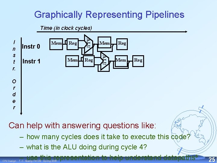
Graphically Representing Pipelines Time (in clock cycles) Instr 1 Reg Mem Reg ALU Instr 0 Mem ALU I n s t r. Mem Reg O r d e r Can help with answering questions like: CPU Design – how many cycles does it take to execute this code? – what is the ALU doing during cycle 4? – use this representation to help understand datapathsº T. -C. Huang / NCUE Spring 2005 25

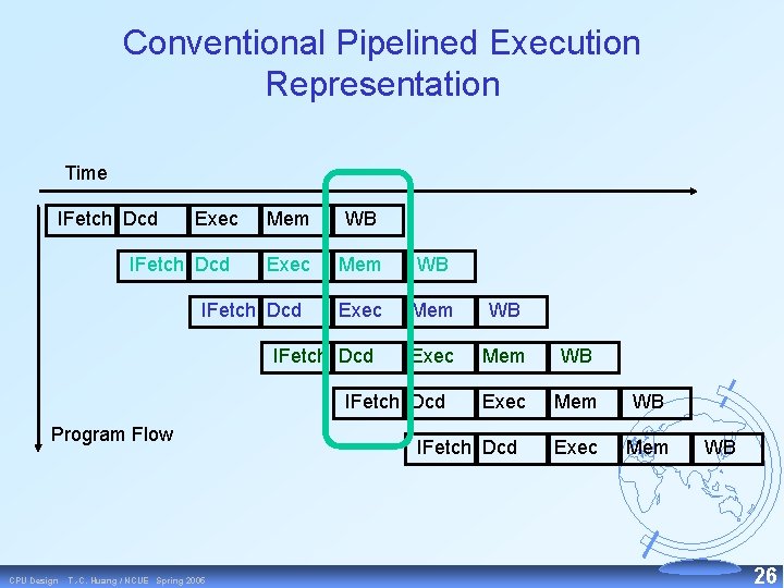
Conventional Pipelined Execution Representation Time IFetch Dcd Exec IFetch Dcd Mem WB Exec Mem WB Exec Mem IFetch Dcd Program Flow CPU Design T. -C. Huang / NCUE Spring 2005 IFetch Dcd WB 26

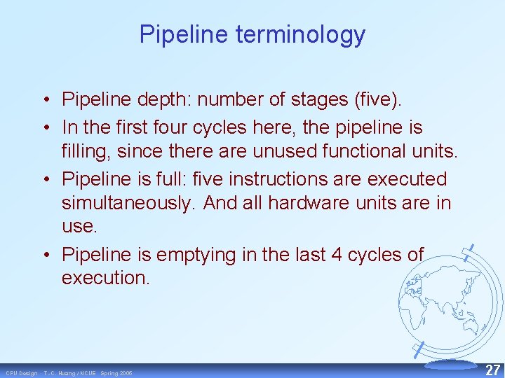
Pipeline terminology • Pipeline depth: number of stages (five). • In the first four cycles here, the pipeline is filling, since there are unused functional units. • Pipeline is full: five instructions are executed simultaneously. And all hardware units are in use. • Pipeline is emptying in the last 4 cycles of execution. CPU Design T. -C. Huang / NCUE Spring 2005 27

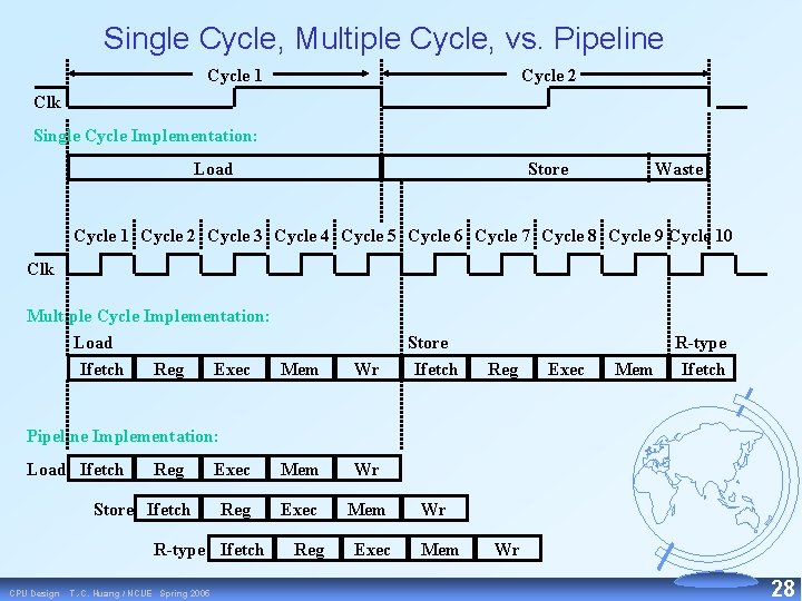
Single Cycle, Multiple Cycle, vs. Pipeline Cycle 1 Cycle 2 Clk Single Cycle Implementation: Load Store Waste Cycle 1 Cycle 2 Cycle 3 Cycle 4 Cycle 5 Cycle 6 Cycle 7 Cycle 8 Cycle 9 Cycle 10 Clk Multiple Cycle Implementation: Load Ifetch Reg Exec Mem Wr Store Ifetch Reg Exec Mem R-type Ifetch Pipeline Implementation: Load Ifetch Reg Store Ifetch Exec Mem Wr Reg Exec Mem R-type Ifetch CPU Design T. -C. Huang / NCUE Spring 2005 Reg Exec Wr Mem Wr 28

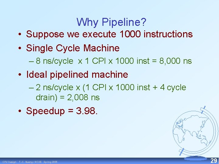
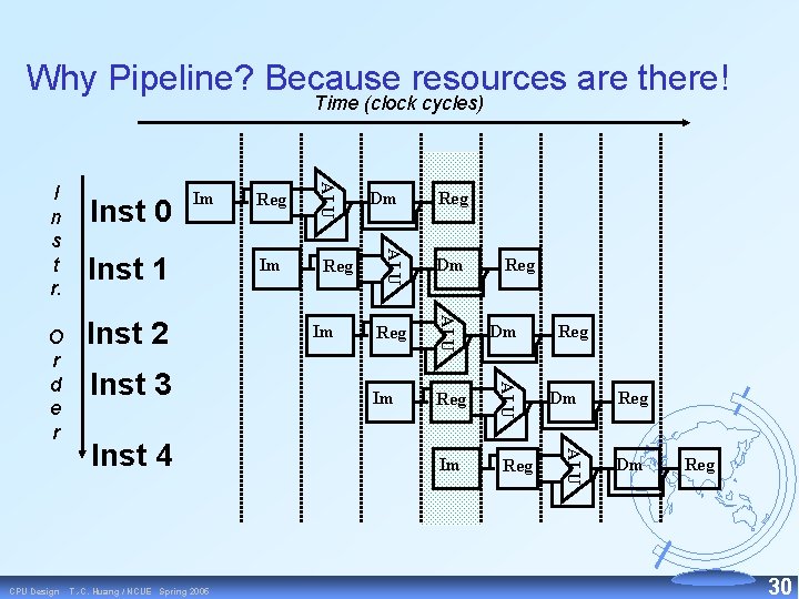
Why Pipeline? • Suppose we execute 1000 instructions • Single Cycle Machine – 8 ns/cycle x 1 CPI x 1000 inst = 8, 000 ns • Ideal pipelined machine – 2 ns/cycle x (1 CPI x 1000 inst + 4 cycle drain) = 2, 008 ns • Speedup = 3. 98. CPU Design T. -C. Huang / NCUE Spring 2005 29

Why Pipeline? Because resources are there! Time (clock cycles) Inst 2 Inst 3 T. -C. Huang / NCUE Spring 2005 Reg Im Reg Dm Im Reg Reg Dm ALU Inst 4 Im Dm ALU Inst 1 Reg ALU CPU Design Im ALU O r d e r Inst 0 ALU I n s t r. Reg Dm Reg 30

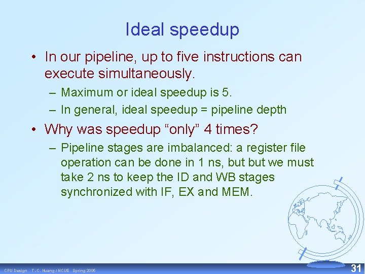
Ideal speedup • In our pipeline, up to five instructions can execute simultaneously. – Maximum or ideal speedup is 5. – In general, ideal speedup = pipeline depth • Why was speedup “only” 4 times? – Pipeline stages are imbalanced: a register file operation can be done in 1 ns, but we must take 2 ns to keep the ID and WB stages synchronized with IF, EX and MEM. CPU Design T. -C. Huang / NCUE Spring 2005 31

Pipelined CPU implementation CPU Design T. -C. Huang / NCUE Spring 2005 32

Hardware for pipelining • A pipelined processor needs to duplicate elements that are used simultaneously. • One single register file to support both ID and WB stages: – “read” and “write” to the register file can occur in the same cycle • Registers are really just lots of edge triggered flip flops. • They always produce outputs (their current value), so they can always be read. • A write will not take effect until the next clock edge. CPU Design T. -C. Huang / NCUE Spring 2005 33

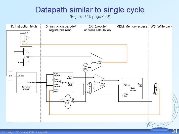
Datapath similar to single cycle (Figure 6. 10 page 450) CPU Design T. -C. Huang / NCUE Spring 2005 34

What has been changed? • Few changes from the original single cycle datapath: – muxes are smaller – data memory has only one address input. The actual memory operation can be determined by the Mem. Read and Mem. Write control signals. • Datapath components have been moved around. CPU Design T. -C. Huang / NCUE Spring 2005 35

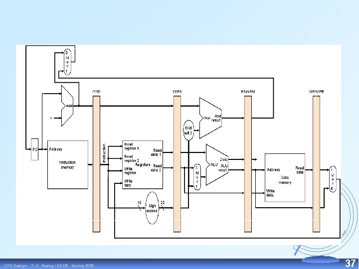
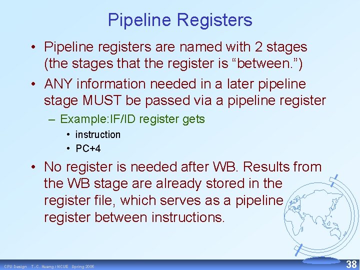
Datapath • Instruction execution is divided into multiple cycles. • In general, data moves from left to right in the datapath. • Several instructions share datapath, but each instruction is in a different pipeline stage. • Information computed during one cycle may be needed in a later cycle. • Like multicycle implementation, we need registers between stages to hold current state of instruction. CPU Design T. -C. Huang / NCUE Spring 2005 36

CPU Design T. -C. Huang / NCUE Spring 2005 37

Pipeline Registers • Pipeline registers are named with 2 stages (the stages that the register is “between. ”) • ANY information needed in a later pipeline stage MUST be passed via a pipeline register – Example: IF/ID register gets • instruction • PC+4 • No register is needed after WB. Results from the WB stage are already stored in the register file, which serves as a pipeline register between instructions. CPU Design T. -C. Huang / NCUE Spring 2005 38

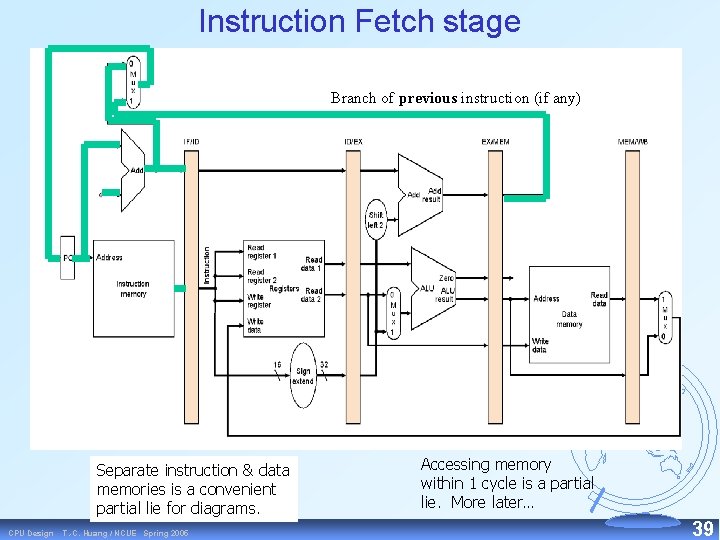
Instruction Fetch stage Branch of previous instruction (if any) Separate instruction & data memories is a convenient partial lie for diagrams. CPU Design T. -C. Huang / NCUE Spring 2005 Accessing memory within 1 cycle is a partial lie. More later… 39

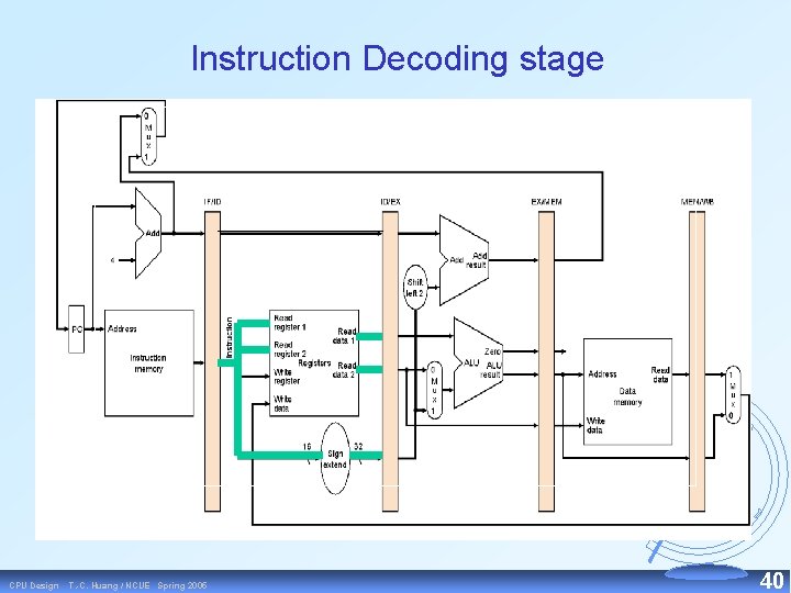
Instruction Decoding stage CPU Design T. -C. Huang / NCUE Spring 2005 40

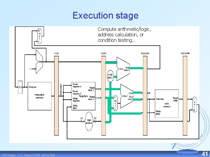
Execution stage Compute arithmetic/logic, address calculation, or condition testing… CPU Design T. -C. Huang / NCUE Spring 2005 41

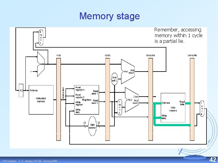
Memory stage Remember, accessing memory within 1 cycle is a partial lie. CPU Design T. -C. Huang / NCUE Spring 2005 42

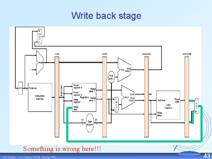
Write back stage Something is wrong here!!! CPU Design T. -C. Huang / NCUE Spring 2005 43

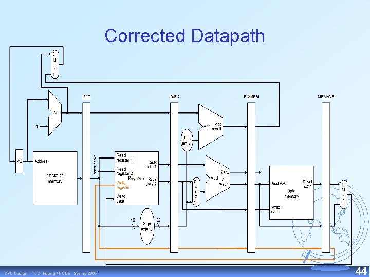
Corrected Datapath CPU Design T. -C. Huang / NCUE Spring 2005 44

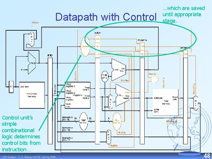
What about control signals? • Control signals are generated in the same way as in the single cycle processor: after the instruction is fetched, the processor can decode the instruction and generate the appropriate control signals. – Controls signals are generated no earlier than the ID stage. • These signals have to be propagated along with the instruction itself, through the rest of the pipeline. CPU Design T. -C. Huang / NCUE Spring 2005 45

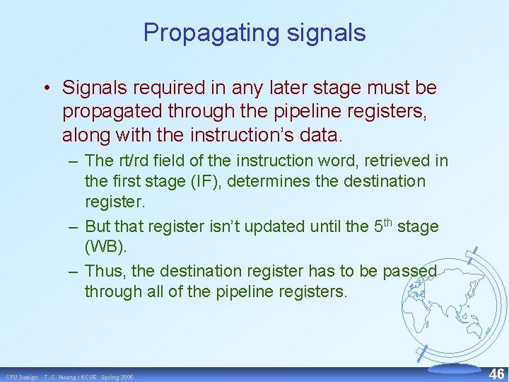
Propagating signals • Signals required in any later stage must be propagated through the pipeline registers, along with the instruction’s data. – The rt/rd field of the instruction word, retrieved in the first stage (IF), determines the destination register. – But that register isn’t updated until the 5 th stage (WB). – Thus, the destination register has to be passed through all of the pipeline registers. CPU Design T. -C. Huang / NCUE Spring 2005 46

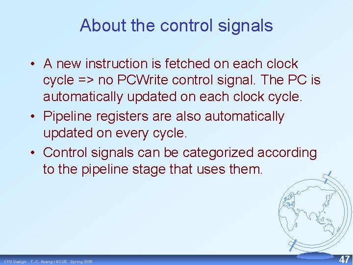
About the control signals • A new instruction is fetched on each clock cycle => no PCWrite control signal. The PC is automatically updated on each clock cycle. • Pipeline registers are also automatically updated on every cycle. • Control signals can be categorized according to the pipeline stage that uses them. CPU Design T. -C. Huang / NCUE Spring 2005 47

Datapath with Control …which are saved until appropriate stage. Control unit’s simple combinational logic determines control bits from instruction… CPU Design T. -C. Huang / NCUE Spring 2005 48

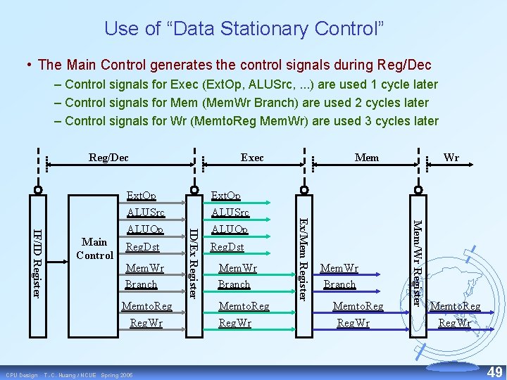
Use of “Data Stationary Control” • The Main Control generates the control signals during Reg/Dec – Control signals for Exec (Ext. Op, ALUSrc, . . . ) are used 1 cycle later – Control signals for Mem (Mem. Wr Branch) are used 2 cycles later – Control signals for Wr (Memto. Reg Mem. Wr) are used 3 cycles later Reg/Dec Mem. Wr Branch Memto. Reg. Wr CPU Design T. -C. Huang / NCUE Spring 2005 Reg. Dst Mem. Wr Branch Memto. Reg Reg. Wr Wr Mem/Wr Register Reg. Dst Ext. Op ALUSrc ALUOp Mem Ex/Mem Register Main Control ID/Ex Register IF/ID Register Ext. Op ALUSrc ALUOp Exec Memto. Reg. Wr 49

Instruction set architectures and pipelining • The MIPS instruction set is especially designed for easy pipelining: – All instructions are one word long, so the IF stage just need to read one word on every clock cycle. – Fields are in the same position in different instruction formats. – MIPS uses a load store, or register to register, architecture, where arithmetic operations cannot contain memory references. CPU Design T. -C. Huang / NCUE Spring 2005 50

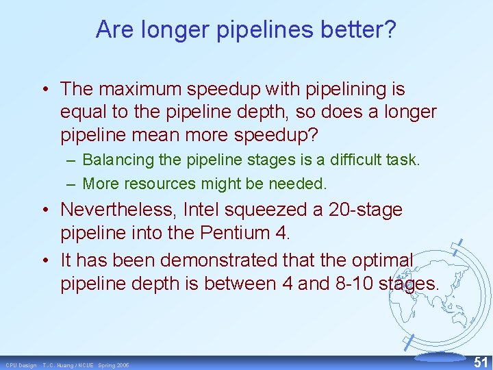
Are longer pipelines better? • The maximum speedup with pipelining is equal to the pipeline depth, so does a longer pipeline mean more speedup? – Balancing the pipeline stages is a difficult task. – More resources might be needed. • Nevertheless, Intel squeezed a 20 stage pipeline into the Pentium 4. • It has been demonstrated that the optimal pipeline depth is between 4 and 8 10 stages. CPU Design T. -C. Huang / NCUE Spring 2005 51

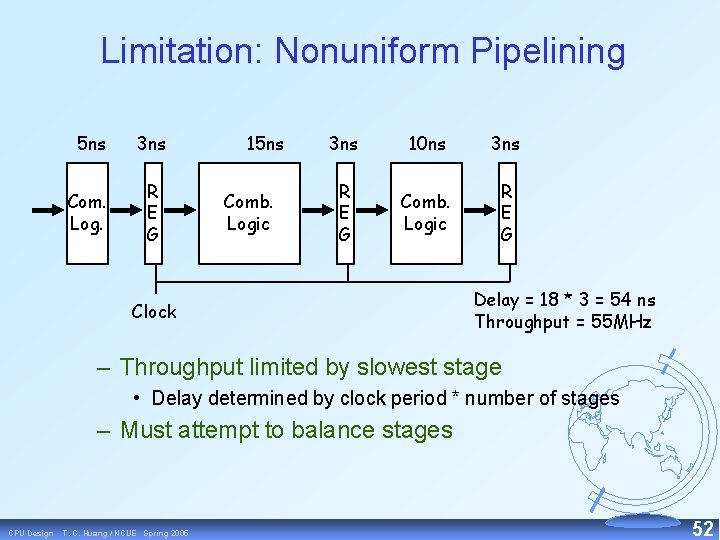
Limitation: Nonuniform Pipelining 5 ns 3 ns Com. Log. R E G 15 ns Comb. Logic 3 ns 10 ns 3 ns R E G Comb. Logic R E G Clock Delay = 18 * 3 = 54 ns Throughput = 55 MHz – Throughput limited by slowest stage • Delay determined by clock period * number of stages – Must attempt to balance stages CPU Design T. -C. Huang / NCUE Spring 2005 52

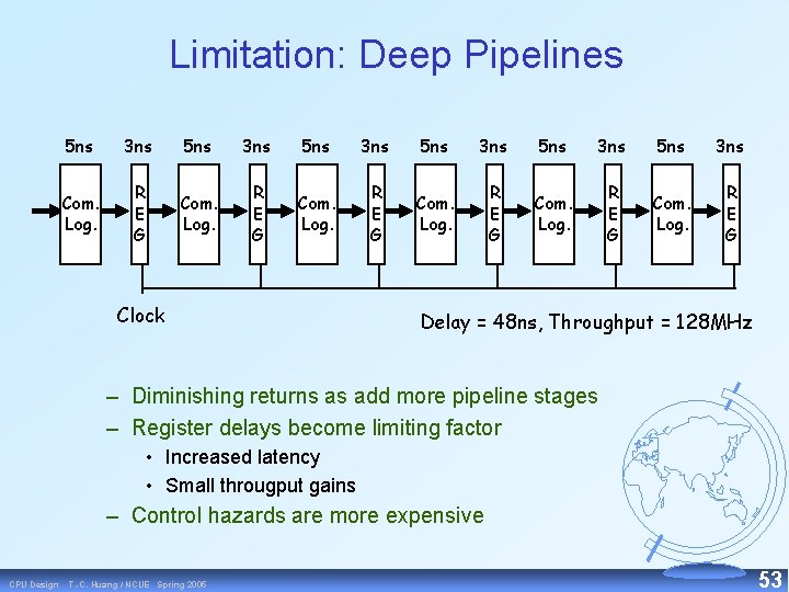
Limitation: Deep Pipelines 5 ns 3 ns 5 ns 3 ns Com. Log. R E G Clock Delay = 48 ns, Throughput = 128 MHz – Diminishing returns as add more pipeline stages – Register delays become limiting factor • Increased latency • Small througput gains – Control hazards are more expensive CPU Design T. -C. Huang / NCUE Spring 2005 53

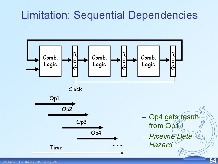
Limitation: Sequential Dependencies R E G Comb. Logic R E G Clock Op 1 Op 2 Op 3 Op 4 Time CPU Design T. -C. Huang / NCUE Spring 2005 • • • – Op 4 gets result from Op 1 ! – Pipeline Data Hazard 54

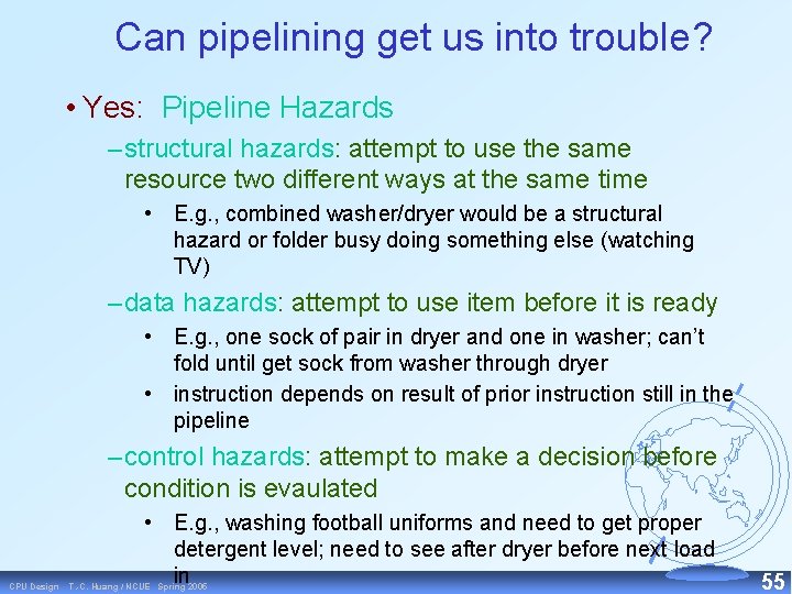
Can pipelining get us into trouble? • Yes: Pipeline Hazards – structural hazards: attempt to use the same resource two different ways at the same time • E. g. , combined washer/dryer would be a structural hazard or folder busy doing something else (watching TV) – data hazards: attempt to use item before it is ready • E. g. , one sock of pair in dryer and one in washer; can’t fold until get sock from washer through dryer • instruction depends on result of prior instruction still in the pipeline – control hazards: attempt to make a decision before condition is evaulated CPU Design • E. g. , washing football uniforms and need to get proper detergent level; need to see after dryer before next load in T. -C. Huang / NCUE Spring 2005 55

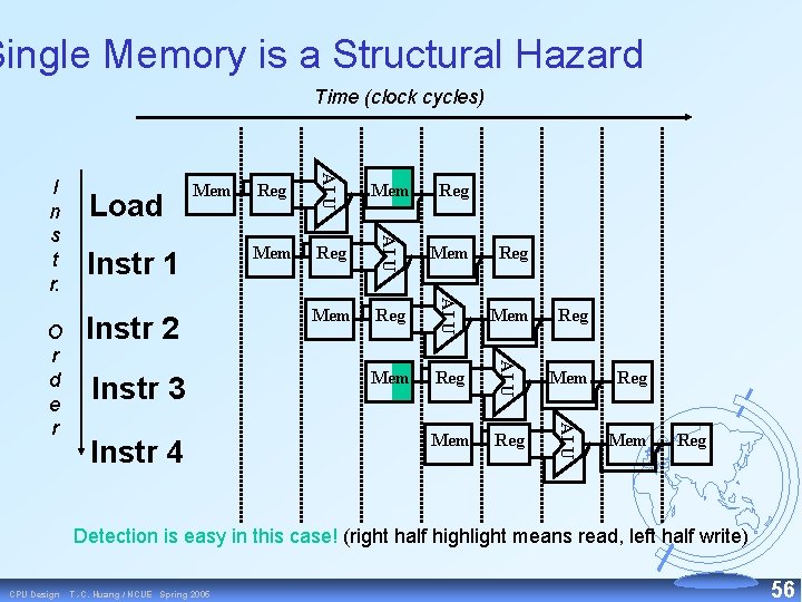
Single Memory is a Structural Hazard Time (clock cycles) Instr 4 Reg Mem Reg Mem Reg ALU Instr 3 Reg ALU Instr 2 Mem ALU Instr 1 Reg ALU O r d e r Load Mem ALU I n s t r. Mem Reg Detection is easy in this case! (right half highlight means read, left half write) CPU Design T. -C. Huang / NCUE Spring 2005 56

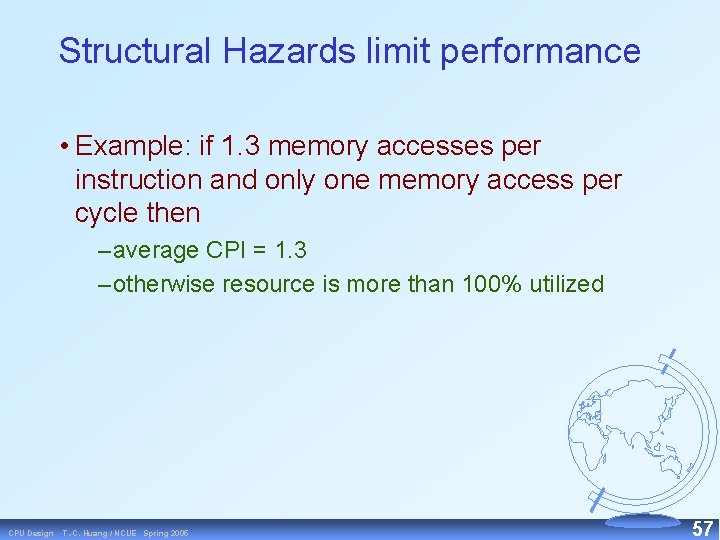
Structural Hazards limit performance • Example: if 1. 3 memory accesses per instruction and only one memory access per cycle then – average CPI = 1. 3 – otherwise resource is more than 100% utilized CPU Design T. -C. Huang / NCUE Spring 2005 57

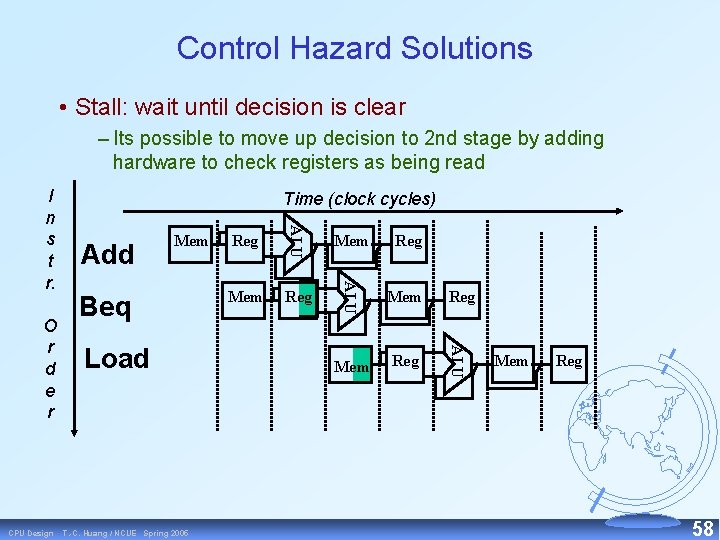
Control Hazard Solutions • Stall: wait until decision is clear – Its possible to move up decision to 2 nd stage by adding hardware to check registers as being read Beq Load T. -C. Huang / NCUE Spring 2005 Reg Mem Reg ALU CPU Design Add Mem ALU O r d e r Time (clock cycles) ALU I n s t r. Mem Reg 58

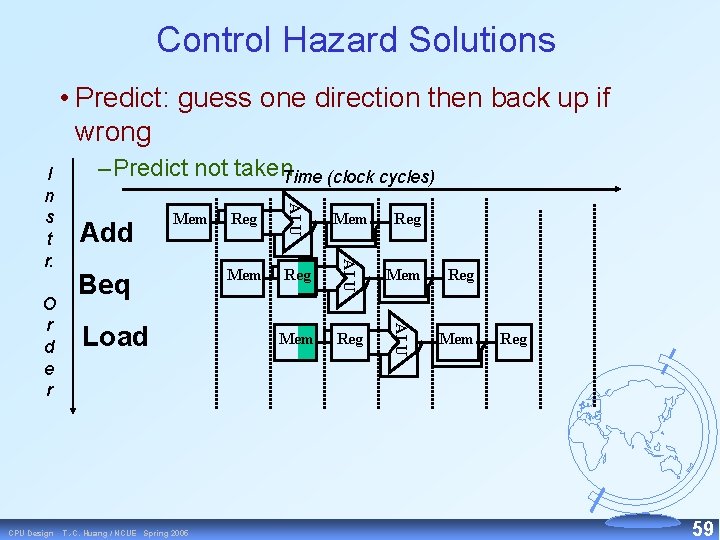
Control Hazard Solutions • Predict: guess one direction then back up if wrong Beq Load T. -C. Huang / NCUE Spring 2005 Reg Mem Reg ALU CPU Design Add Mem ALU O r d e r – Predict not taken. Time (clock cycles) ALU I n s t r. Mem Reg 59

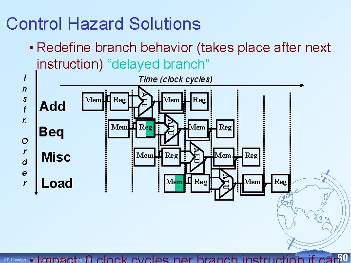
Control Hazard Solutions • Redefine branch behavior (takes place after next instruction) “delayed branch” Beq Misc T. -C. Huang / NCUE Spring 2005 Mem Reg Mem Reg ALU Load Reg ALU CPU Design Add Mem ALU O r d e r Time (clock cycles) ALU I n s t r. Reg Mem Reg 60

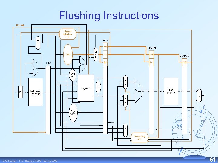
Flushing Instructions CPU Design T. -C. Huang / NCUE Spring 2005 61

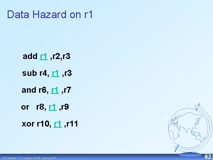
Data Hazard on r 1 add r 1 , r 2, r 3 sub r 4, r 1 , r 3 and r 6, r 1 , r 7 or r 8, r 1 , r 9 xor r 10, r 11 CPU Design T. -C. Huang / NCUE Spring 2005 62

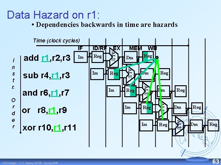
Data Hazard on r 1: • Dependencies backwards in time are hazards xor r 10, r 11 T. -C. Huang / NCUE Spring 2005 Reg Dm Im Reg ALU or r 8, r 1, r 9 WB ALU CPU Design and r 6, r 1, r 7 MEM ALU O r d e r sub r 4, r 1, r 3 Im EX ALU I n s t r. add r 1, r 2, r 3 ID/RF ALU Time (clock cycles) IF Reg Reg Dm Reg 63

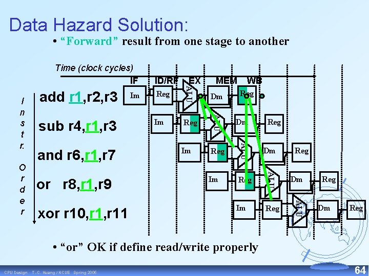
Data Hazard Solution: • “Forward” result from one stage to another xor r 10, r 11 Reg Dm Im Reg ALU or r 8, r 1, r 9 WB ALU and r 6, r 1, r 7 MEM ALU O r d e r sub r 4, r 1, r 3 Im EX ALU I n s t r. add r 1, r 2, r 3 ID/RF ALU Time (clock cycles) IF Reg Reg Dm Reg • “or” OK if define read/write properly CPU Design T. -C. Huang / NCUE Spring 2005 64

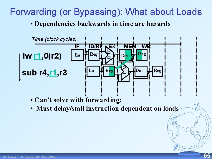
Forwarding (or Bypassing): What about Loads • Dependencies backwards in time are hazards sub r 4, r 1, r 3 Im EX MEM Reg Dm Im Reg ALU lw r 1, 0(r 2) ID/RF ALU Time (clock cycles) IF WB Reg Dm Reg • Can’t solve with forwarding: • Must delay/stall instruction dependent on loads CPU Design T. -C. Huang / NCUE Spring 2005 65

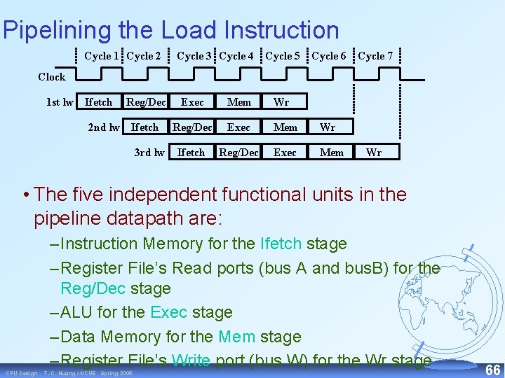
Pipelining the Load Instruction Cycle 1 Cycle 2 Cycle 3 Cycle 4 Cycle 5 Cycle 6 Cycle 7 Clock 1 st lw Ifetch Reg/Dec 2 nd lw Ifetch 3 rd lw Exec Mem Wr Reg/Dec Exec Mem Wr Ifetch Reg/Dec Exec Mem Wr • The five independent functional units in the pipeline datapath are: – Instruction Memory for the Ifetch stage – Register File’s Read ports (bus A and bus. B) for the Reg/Dec stage – ALU for the Exec stage – Data Memory for the Mem stage – Register File’s Write port (bus W) for the Wr stage CPU Design T. -C. Huang / NCUE Spring 2005 66

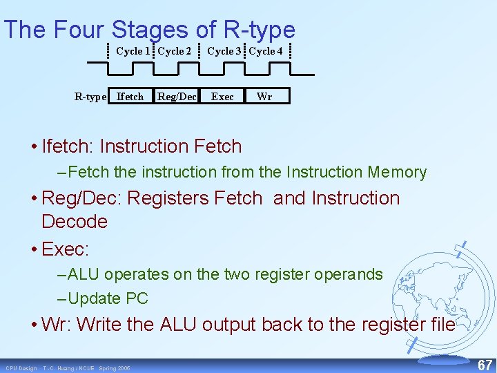
The Four Stages of R type Cycle 1 Cycle 2 R-type Ifetch Reg/Dec Cycle 3 Cycle 4 Exec Wr • Ifetch: Instruction Fetch – Fetch the instruction from the Instruction Memory • Reg/Dec: Registers Fetch and Instruction Decode • Exec: – ALU operates on the two register operands – Update PC • Wr: Write the ALU output back to the register file CPU Design T. -C. Huang / NCUE Spring 2005 67

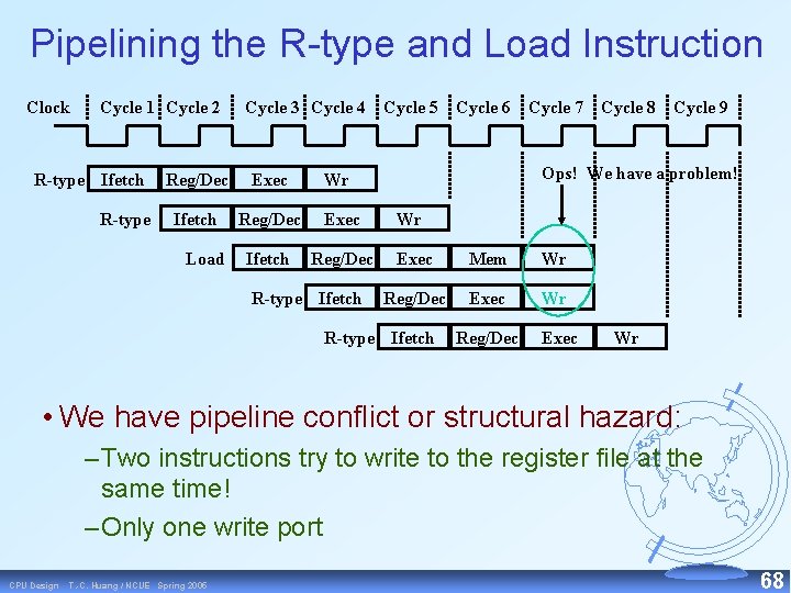
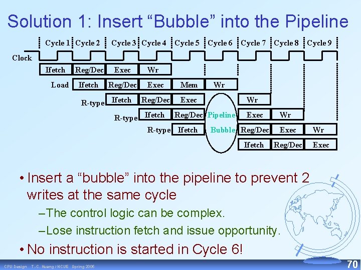
Pipelining the R type and Load Instruction Clock Cycle 1 Cycle 2 R-type Ifetch R-type Cycle 3 Cycle 4 Cycle 5 Cycle 6 Cycle 7 Cycle 8 Cycle 9 Reg/Dec Exec Ifetch Reg/Dec Load Ops! We have a problem! Wr R-type Ifetch Wr Exec Mem Wr Reg/Dec Exec Wr R-type Ifetch Reg/Dec Exec Wr • We have pipeline conflict or structural hazard: – Two instructions try to write to the register file at the same time! – Only one write port CPU Design T. -C. Huang / NCUE Spring 2005 68

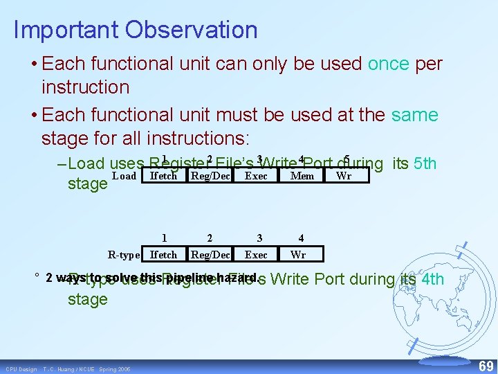
Important Observation • Each functional unit can only be used once per instruction • Each functional unit must be used at the same stage for all instructions: 1 2 5 – Load uses Register File’s 3 Write 4 Port during its 5 th Load Ifetch Reg/Dec Exec Mem Wr stage 1 R-type Ifetch 2 Reg/Dec 3 Exec ° 2 ways to solve this. Register pipeline hazard. – R type uses File’s 4 Wr Write Port during its 4 th stage CPU Design T. -C. Huang / NCUE Spring 2005 69

Solution 1: Insert “Bubble” into the Pipeline Cycle 1 Cycle 2 Cycle 3 Cycle 4 Cycle 5 Cycle 6 Cycle 7 Cycle 8 Cycle 9 Clock Ifetch Load Reg/Dec Exec Ifetch Reg/Dec R-type Ifetch Wr Exec Mem Reg/Dec Exec Wr Wr R-type Ifetch Reg/Dec Pipeline Exec R-type Ifetch Bubble Reg/Dec Ifetch Wr Exec Reg/Dec Wr Exec • Insert a “bubble” into the pipeline to prevent 2 writes at the same cycle – The control logic can be complex. – Lose instruction fetch and issue opportunity. • No instruction is started in Cycle 6! CPU Design T. -C. Huang / NCUE Spring 2005 70

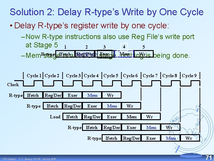
Solution 2: Delay R type’s Write by One Cycle • Delay R type’s register write by one cycle: – Now R type instructions also use Reg File’s write port at Stage 5 1 4 2 3 5 Exec Mem Reg/Dec stage: Wris being done. – Mem. R-type stage. Ifetch is a NOOP nothing Cycle 1 Cycle 2 Cycle 3 Cycle 4 Cycle 5 Cycle 6 Cycle 7 Cycle 8 Cycle 9 Clock R-type Ifetch R-type Reg/Dec Exec Mem Wr Ifetch Reg/Dec Exec Mem Wr Reg/Dec Exec Mem Load R-type Ifetch CPU Design T. -C. Huang / NCUE Spring 2005 Wr 71

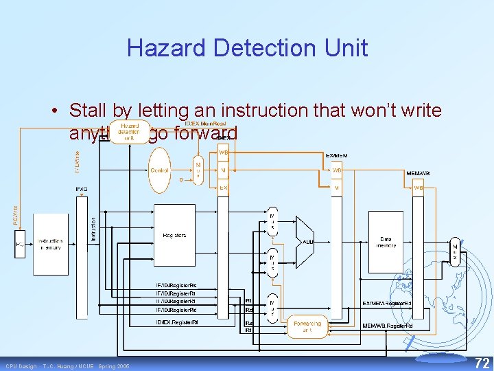
Hazard Detection Unit • Stall by letting an instruction that won’t write anything go forward CPU Design T. -C. Huang / NCUE Spring 2005 72

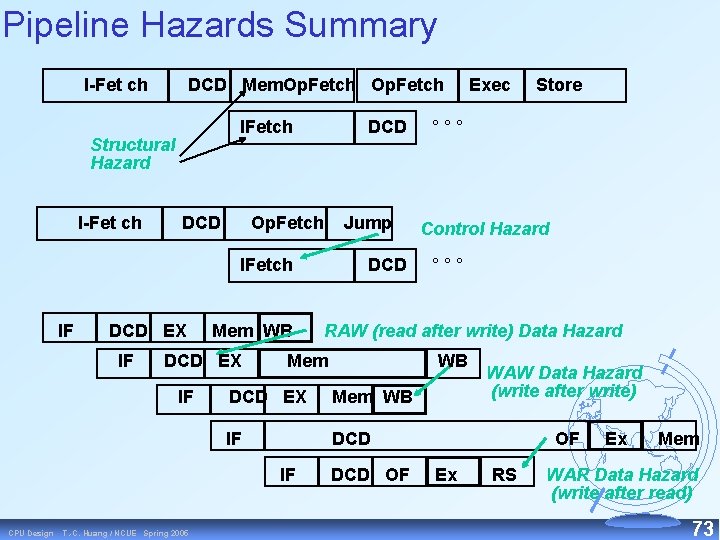
Pipeline Hazards Summary I-Fet ch DCD Mem. Op. Fetch IFetch Structural Hazard I-Fet ch DCD Op. Fetch Jump IFetch IF DCD EX IF Mem WB DCD EX IF T. -C. Huang / NCUE Spring 2005 Store °°° Control Hazard °°° RAW (read after write) Data Hazard Mem WB DCD EX Mem WB IF DCD IF CPU Design DCD Exec DCD OF WAW Data Hazard (write after write) OF Ex RS Ex Mem WAR Data Hazard (write after read) 73

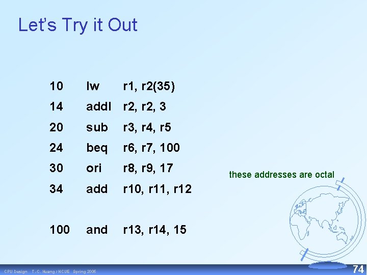
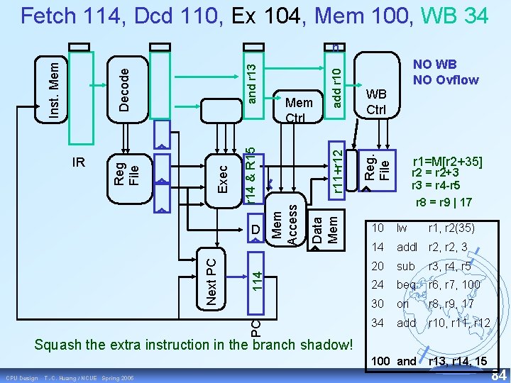
Let’s Try it Out CPU Design 10 lw 14 add. I r 2, 3 20 sub r 3, r 4, r 5 24 beq r 6, r 7, 100 30 ori r 8, r 9, 17 34 add r 10, r 11, r 12 100 and r 13, r 14, 15 T. -C. Huang / NCUE Spring 2005 r 1, r 2(35) these addresses are octal 74

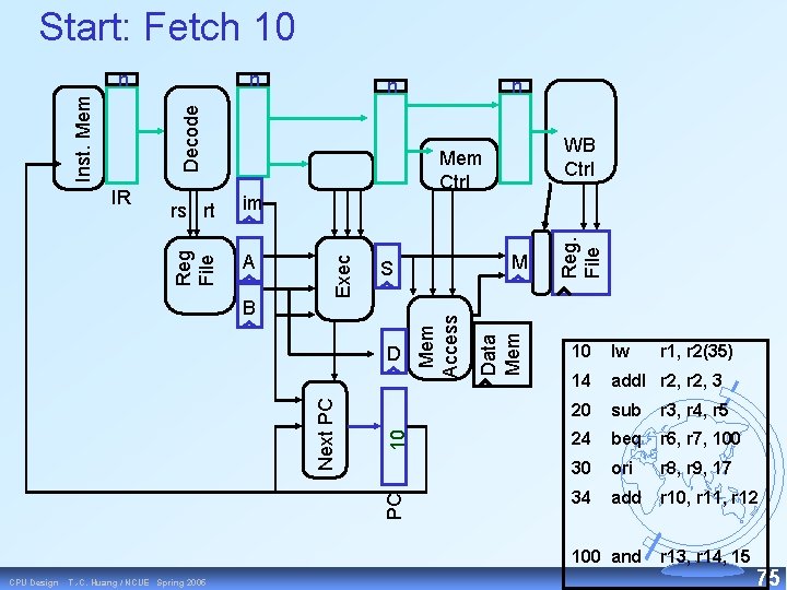
Start: Fetch 10 n B PC 10 D Next PC M S Data Mem Access im WB Ctrl Mem Ctrl Exec rs rt Reg File IR n Reg. File n Decode Inst. Mem n 10 lw 14 add. I r 2, 3 20 sub r 3, r 4, r 5 24 beq r 6, r 7, 100 30 ori r 8, r 9, 17 34 add r 10, r 11, r 12 100 and CPU Design T. -C. Huang / NCUE Spring 2005 r 1, r 2(35) r 13, r 14, 15 75

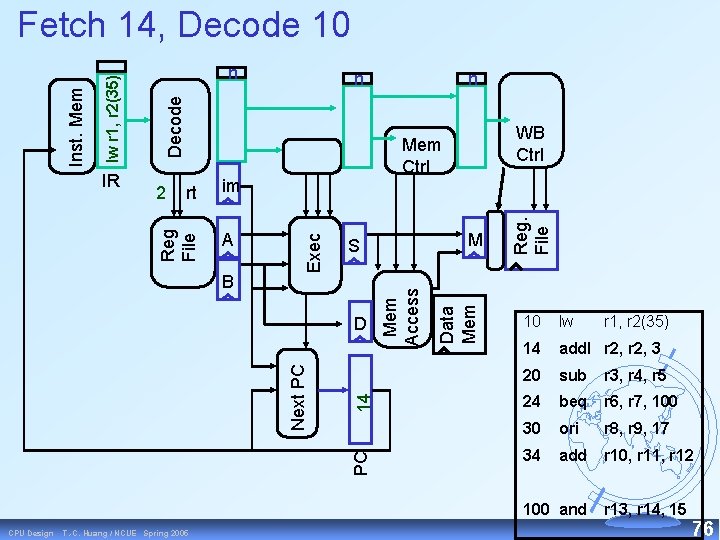
B PC 14 D Next PC M S Data Mem im A WB Ctrl Mem Access rt n Reg. File n Exec 2 Reg File IR n Decode lw r 1, r 2(35) Inst. Mem Fetch 14, Decode 10 10 lw 14 add. I r 2, 3 20 sub r 3, r 4, r 5 24 beq r 6, r 7, 100 30 ori r 8, r 9, 17 34 add r 10, r 11, r 12 100 and CPU Design T. -C. Huang / NCUE Spring 2005 r 1, r 2(35) r 13, r 14, 15 76

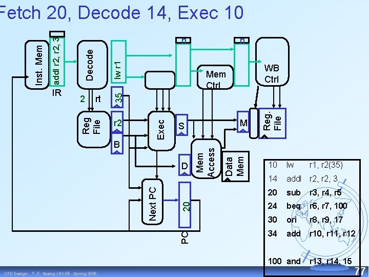
PC 20 Data Mem D Next PC M S Mem Access B WB Ctrl Mem Ctrl Exec r 2 2 n Reg. File lw r 1 Decode rt 35 IR n Reg File add. I r 2, 3 Inst. Mem Fetch 20, Decode 14, Exec 10 10 lw 14 add. I r 2, 3 20 sub r 3, r 4, r 5 24 beq r 6, r 7, 100 30 ori r 8, r 9, 17 34 add r 10, r 11, r 12 100 and CPU Design T. -C. Huang / NCUE Spring 2005 r 1, r 2(35) r 13, r 14, 15 77

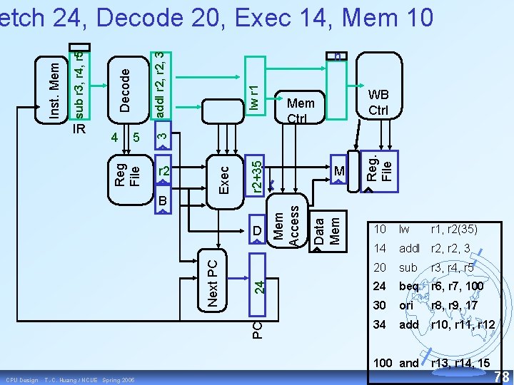
Data Mem Reg. File lw r 1 24 PC Next PC D M Mem Access B WB Ctrl Mem Ctrl r 2+35 r 2 Exec 4 n add. I r 2, 3 Decode 5 3 IR Reg File sub r 3, r 4, r 5 Inst. Mem etch 24, Decode 20, Exec 14, Mem 10 10 lw 14 add. I r 2, 3 20 sub r 3, r 4, r 5 24 beq r 6, r 7, 100 30 ori r 8, r 9, 17 34 add r 10, r 11, r 12 100 and CPU Design T. -C. Huang / NCUE Spring 2005 r 1, r 2(35) r 13, r 14, 15 78
![lw r 1 WB Ctrl Mr 235 Reg File add I r 2 sub lw r 1 WB Ctrl M[r 2+35] Reg. File add. I r 2 sub](https://slidetodoc.com/presentation_image_h2/4c660843383a415a675dfc6103344681/image-79.jpg)
lw r 1 WB Ctrl M[r 2+35] Reg. File add. I r 2 sub r 3 Mem Ctrl 30 PC Next PC D Data Mem r 5 Mem Access r 4 r 2+3 7 Exec 6 Reg File IR Decode beq r 6, r 7 100 Inst. Mem Fetch 30, Dcd 24, Ex 20, Mem 14, WB 10 10 lw 14 add. I r 2, 3 20 sub r 3, r 4, r 5 24 beq r 6, r 7, 100 30 ori r 8, r 9, 17 34 add r 10, r 11, r 12 100 and CPU Design T. -C. Huang / NCUE Spring 2005 r 1, r 2(35) r 13, r 14, 15 79
![Reg File r 1Mr 235 add I r 2 WB Ctrl r 23 sub Reg. File r 1=M[r 2+35] add. I r 2 WB Ctrl r 2+3 sub](https://slidetodoc.com/presentation_image_h2/4c660843383a415a675dfc6103344681/image-80.jpg)
Reg. File r 1=M[r 2+35] add. I r 2 WB Ctrl r 2+3 sub r 3 beq 34 PC Next PC Data Mem D Mem Access r 7 r 4 r 5 r 6 Exec xx Mem Ctrl 100 9 Reg File IR Decode ori r 8, r 9 17 Inst. Mem Fetch 34, Dcd 30, Ex 24, Mem 20, WB 14 10 lw 14 add. I r 2, 3 20 sub r 3, r 4, r 5 24 beq r 6, r 7, 100 30 ori r 8, r 9, 17 34 add r 10, r 11, r 12 100 and CPU Design T. -C. Huang / NCUE Spring 2005 r 1, r 2(35) r 13, r 14, 15 80

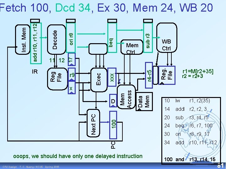
ooops, we should have only one delayed instruction T. -C. Huang / NCUE Spring 2005 WB Ctrl r 1=M[r 2+35] Reg. File r 4 r 5 Data Mem xxx 100 PC Next PC D Mem Access x CPU Design sub r 3 beq ori r 8 Decode Mem Ctrl 17 r 9 Exec IR 11 12 Reg File add r 10, r 11, r 12 Inst. Mem Fetch 100, Dcd 34, Ex 30, Mem 24, WB 20 r 2 = r 2+3 10 lw r 1, r 2(35) 14 add. I r 2, 3 20 sub r 3, r 4, r 5 24 beq r 6, r 7, 100 30 ori r 8, r 9, 17 34 add r 10, r 11, r 12 100 and r 13, r 14, 15 81

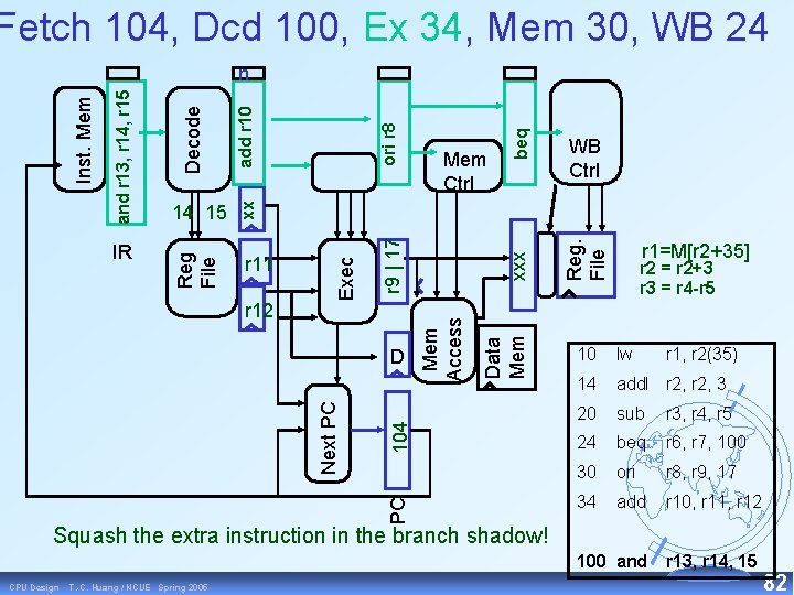
Fetch 104, Dcd 100, Ex 34, Mem 30, WB 24 beq ori r 8 add r 10 WB Ctrl r 1=M[r 2+35] Reg. File xxx Data Mem 104 PC Next PC D Mem Access r 12 r 9 | 17 Decode Mem Ctrl xx r 11 Exec IR 14 15 Reg File and r 13, r 14, r 15 Inst. Mem n r 2 = r 2+3 r 3 = r 4 -r 5 10 lw r 1, r 2(35) 14 add. I r 2, 3 20 sub r 3, r 4, r 5 24 beq r 6, r 7, 100 30 ori r 8, r 9, 17 34 add r 10, r 11, r 12 100 and r 13, r 14, 15 Squash the extra instruction in the branch shadow! CPU Design T. -C. Huang / NCUE Spring 2005 82

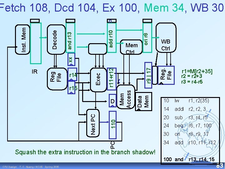
Fetch 108, Dcd 104, Ex 100, Mem 34, WB 30 ori r 8 add r 10 and r 13 Mem Ctrl WB Ctrl r 1=M[r 2+35] Reg. File r 9 | 17 Data Mem 110 PC Next PC D Mem Access r 15 r 11+r 12 r 14 Exec IR Reg File xx Decode Inst. Mem n r 2 = r 2+3 r 3 = r 4 -r 5 10 lw r 1, r 2(35) 14 add. I r 2, 3 20 sub r 3, r 4, r 5 24 beq r 6, r 7, 100 30 ori r 8, r 9, 17 34 add r 10, r 11, r 12 100 and r 13, r 14, 15 Squash the extra instruction in the branch shadow! CPU Design T. -C. Huang / NCUE Spring 2005 83

Fetch 114, Dcd 110, Ex 104, Mem 100, WB 34 NO WB NO Ovflow WB Ctrl r 1=M[r 2+35] Reg. File add r 10 r 11+r 12 Data Mem 114 PC Next PC D Mem Ctrl Mem Access and r 13 r 14 & R 15 Exec IR Reg File Decode Inst. Mem n r 2 = r 2+3 r 3 = r 4 -r 5 r 8 = r 9 | 17 10 lw r 1, r 2(35) 14 add. I r 2, 3 20 sub r 3, r 4, r 5 24 beq r 6, r 7, 100 30 ori r 8, r 9, 17 34 add r 10, r 11, r 12 100 and r 13, r 14, 15 Squash the extra instruction in the branch shadow! CPU Design T. -C. Huang / NCUE Spring 2005 84

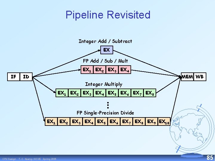
Pipeline Revisited Integer Add / Subtract EX FP Add / Sub / Mult IF EX 1 EX 2 EX 3 EX 4 ID MEM WB Integer Multiply EX 1 EX 2 EX 3 EX 4 EX 5 EX 6 EX 7 EX 8 . . . FP Single-Precision Divide EX 1 EX 2 EX 3 EX 4 EX 5 EX 6 EX 7 EX 8 EX 9 EX 10 CPU Design T. -C. Huang / NCUE Spring 2005 85

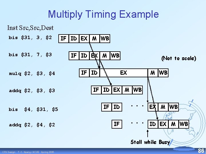
Multiply Timing Example Inst Src, Dest bis $31, 3, $2 bis $31, 7, $3 mulq $2, $3, $4 addq $2, $3 bis $4, $31, $5 addq $2, $4, $2 IF ID EX M WB IF ID (Not to scale) EX M WB IF ID IF • • • EX M WB • • • ID EX M WB Stall while Busy CPU Design T. -C. Huang / NCUE Spring 2005 86

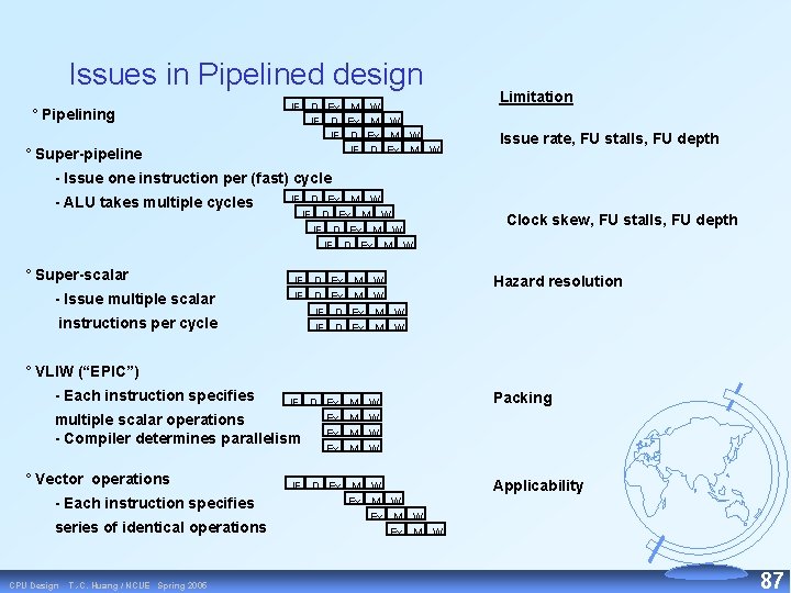
Issues in Pipelined design ° Pipelining ° Super-pipeline IF D Ex M IF D Ex IF D IF W M W Ex M W D Ex M W Limitation Issue rate, FU stalls, FU depth - Issue one instruction per (fast) cycle - ALU takes multiple cycles ° Super-scalar - Issue multiple scalar instructions per cycle IF D Ex M W IF D Ex IF D M M Ex Ex W W M W Clock skew, FU stalls, FU depth Hazard resolution ° VLIW (“EPIC”) - Each instruction specifies IF D Ex Ex multiple scalar operations Ex - Compiler determines parallelism Ex ° Vector operations - Each instruction specifies series of identical operations CPU Design T. -C. Huang / NCUE Spring 2005 M M W W IF D Ex M W Packing Applicability 87

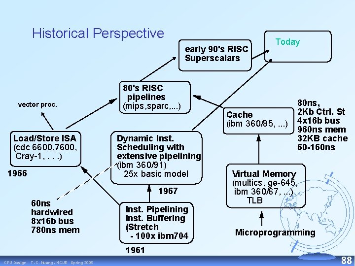
Historical Perspective early 90's RISC Superscalars vector proc. Load/Store ISA (cdc 6600, 7600, Cray 1, . . . ) 1966 80's RISC pipelines (mips, sparc, . . . ) Dynamic Inst. Scheduling with extensive pipelining (ibm 360/91) 25 x basic model 1967 60 ns hardwired 8 x 16 b bus 780 ns mem Inst. Pipelining Inst. Buffering (Stretch - 100 x ibm 704 Today Cache (ibm 360/85, . . . ) 80 ns, 2 Kb Ctrl. St 4 x 16 b bus 960 ns mem 32 KB cache 60 -160 ns Virtual Memory (multics, ge 645, ibm 360/67, . . . ) TLB Microprogramming 1961 CPU Design T. -C. Huang / NCUE Spring 2005 88

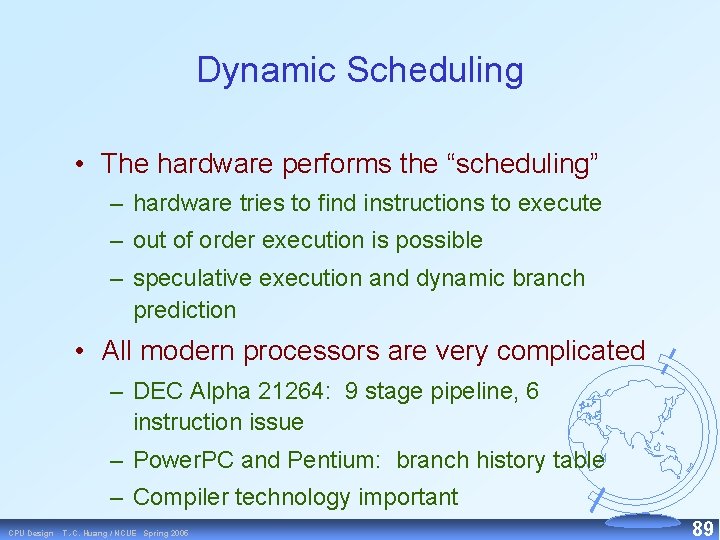
Dynamic Scheduling • The hardware performs the “scheduling” – hardware tries to find instructions to execute – out of order execution is possible – speculative execution and dynamic branch prediction • All modern processors are very complicated – DEC Alpha 21264: 9 stage pipeline, 6 instruction issue – Power. PC and Pentium: branch history table – Compiler technology important CPU Design T. -C. Huang / NCUE Spring 2005 89

Summary • Pipelining is a fundamental concept – multiple steps using distinct resources • Utilize capabilities of the Datapath by pipelined instruction processing – start next instruction while working on the current one – limited by length of longest stage (plus fill/flush) – detect and resolve hazards CPU Design T. -C. Huang / NCUE Spring 2005 90

Summary • Pipelining combine ideas from the single and multicycle implementations: – Multiple memories and ALUs are used as in the single cycle datapath. – Instruction execution are divided into stages as in the multicycle datapath. • Multiple stages are supported by pipeline registers, which propagate both data and control information forward to subsequent stages. CPU Design T. -C. Huang / NCUE Spring 2005 91

Summary • What makes it easy – all instructions are the same length – just a few instruction formats – memory operands appear only in loads and stores • What makes it hard? – structural hazards: suppose we had only one memory – control hazards: need to worry about branch instructions – data hazards: an instruction depends on a previous instruction CPU Design T. -C. Huang / NCUE Spring 2005 92

Know-how Ø In the Internet Era, Know how ← Know where Ø However, Know how ≠ Know where Ø Design Philosophy! Source of Creativity Few philosophy shown in reference CPU Design T. -C. Huang / NCUE Spring 2005 93

Rethink Ø How to design the MIPS architecture before it was created? Ø Making up the story: 1. Core based MCU → Large i ROM with small d RAM 2. Core based → Pipeline → 5 stages 3. → Instruction set → Instruction format → 32 bits CPU Design T. -C. Huang / NCUE Spring 2005 94

Project Ø Ø Follow and modify an open core CPU Especially give your design steps And address your philosophy Example 1. 2. 3. 4. 5. 6. CPU Design 8051: familiar MIPS: regular and becoming hot ARM: hot VLIW: special architecture PDP 8: in traditional textbook 8080: compatible to the core of PC T. -C. Huang / NCUE Spring 2005 95