IDDS Testing in Nanometer Technology TsungChu Huang Dept
![Transient Cutoff Current [CCECE 01 Raahemifar] Ø Pattern residue enables the latch Ø However, Transient Cutoff Current [CCECE 01 Raahemifar] Ø Pattern residue enables the latch Ø However,](https://slidetodoc.com/presentation_image_h2/8fb186da3d436af75a7b350878206a2e/image-10.jpg)
![Core IDDQ Test in P 1500 [DAC 02 Ravikumar] Ø Leakage current is divided. Core IDDQ Test in P 1500 [DAC 02 Ravikumar] Ø Leakage current is divided.](https://slidetodoc.com/presentation_image_h2/8fb186da3d436af75a7b350878206a2e/image-11.jpg)
![Shannon Expansion [ATS 05 Ghosh] Ø Adaptively partitioned by input pattern xi. Ø Area Shannon Expansion [ATS 05 Ghosh] Ø Adaptively partitioned by input pattern xi. Ø Area](https://slidetodoc.com/presentation_image_h2/8fb186da3d436af75a7b350878206a2e/image-12.jpg)
![On/Off Current Ratio Ø Ion/Ioff trades delay cost with leakage reduction [ISCA 02 Heo] On/Off Current Ratio Ø Ion/Ioff trades delay cost with leakage reduction [ISCA 02 Heo]](https://slidetodoc.com/presentation_image_h2/8fb186da3d436af75a7b350878206a2e/image-16.jpg)
![Basic Structure: [VLSI-DAT 06] Supply-Gating for Data Retention & Spike Reduction VDD Sp Ø Basic Structure: [VLSI-DAT 06] Supply-Gating for Data Retention & Spike Reduction VDD Sp Ø](https://slidetodoc.com/presentation_image_h2/8fb186da3d436af75a7b350878206a2e/image-21.jpg)
![References [1] [2] [3] [4] [5] [6] [7] [8] European Design and Test Conf. References [1] [2] [3] [4] [5] [6] [7] [8] European Design and Test Conf.](https://slidetodoc.com/presentation_image_h2/8fb186da3d436af75a7b350878206a2e/image-41.jpg)
- Slides: 41

IDDS Testing in Nanometer Technology Tsung-Chu Huang Dept. of Ec. E, Nat’l Changhua U. of Ed. May 6, 2006 NCUE EDA Df. Cnm@VTTF 2006/05/06 T. -C. Huang, NCUE

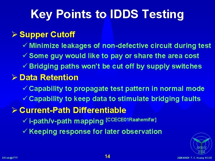
Outline Ø Introduction ü Issue of IDDQ Test in NMT ü Leakage Analysis Ø Previous Work Ø Technological Background Ø Proposed Scheme and Design for IDDS Testing ü Basic Concept and Basic Structure ü Inter-gate IDDS Testing ü Intra-gate IDDS Testing Ø Experimental Results Ø Conclusions Df. Cnm@VTTF 2 NCUE EDA 2006/05/06 T. -C. Huang, NCUE

Outline Ø Introduction ü Issue of IDDQ Test in NMT ü Leakage Analysis Ø Previous Work Ø Technological Background Ø Proposed Scheme and Design for IDDS Testing ü Basic Concept and Basic Structure ü Inter-gate IDDS Testing ü Intra-gate IDDS Testing Ø Experimental Results Ø Conclusions Df. Cnm@VTTF 3 NCUE EDA 2006/05/06 T. -C. Huang, NCUE

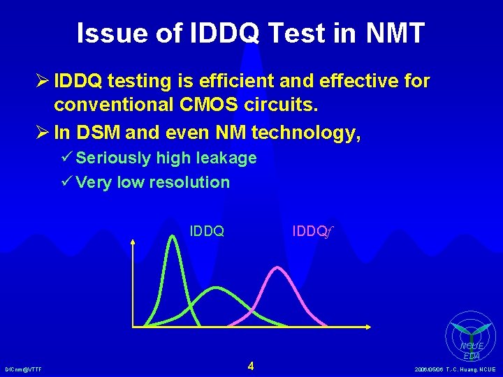
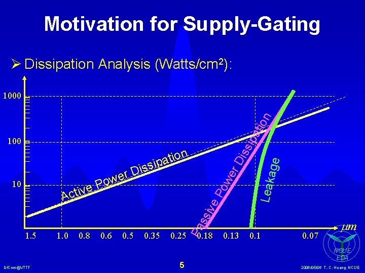
Issue of IDDQ Test in NMT Ø IDDQ testing is efficient and effective for conventional CMOS circuits. Ø In DSM and even NM technology, ü Seriously high leakage ü Very low resolution IDDQf IDDQ Df. Cnm@VTTF 4 NCUE EDA 2006/05/06 T. -C. Huang, NCUE

Motivation for Supply-Gating Ø Dissipation Analysis (Watts/cm 2): ipa tio n 1000 we s i D r we Df. Cnm@VTTF 1. 0 0. 8 0. 6 ss ive 0. 5 0. 35 0. 25 5 Pa 1. 5 Po o P e v i Act 10 0. 18 0. 13 Leak n io t a p si age r. D iss 100 0. 1 0. 07 mm NCUE EDA 2006/05/06 T. -C. Huang, NCUE

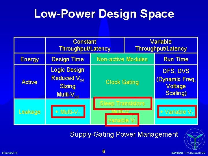
Low-Power Design Space Constant Throughput/Latency Energy Design Time Active Leakage Variable Throughput/Latency Non-active Modules Run Time Logic Design Reduced Vdd Sizing Multi-Vdd Clock Gating DFS, DVS (Dynamic Freq, Voltage Scaling) + Multi-VT Sleep Transistors Multi-Vdd Variable VT + Variable VT Supply-Gating Power Management Df. Cnm@VTTF 6 NCUE EDA 2006/05/06 T. -C. Huang, NCUE

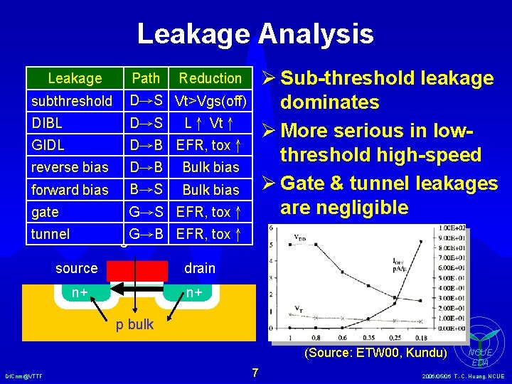
Leakage Analysis Leakage Path Ø Sub-threshold leakage dominates Ø More serious in lowthreshold high-speed Ø Gate & tunnel leakages are negligible Reduction subthreshold D→S Vt>Vgs(off) DIBL D→S GIDL D→B EFR, tox↑ reverse bias D→B Bulk bias forward bias B→S Bulk bias gate G→S EFR, tox↑ L↑ Vt↑ G→B EFR, tox↑ gate tunnel source drain n+ n+ p bulk (Source: ETW 00, Kundu) Df. Cnm@VTTF 7 NCUE EDA 2006/05/06 T. -C. Huang, NCUE

Outline Ø Introduction ü Issue of IDDQ Test in NMT ü Leakage Analysis Ø Previous Work Ø Technical Background Ø Proposed Scheme and Design for IDDS Testing ü Basic Concept and Basic Structure ü Inter-gate IDDS Testing ü Intra-gate IDDS Testing Ø Experimental Results Ø Conclusions Df. Cnm@VTTF 8 NCUE EDA 2006/05/06 T. -C. Huang, NCUE

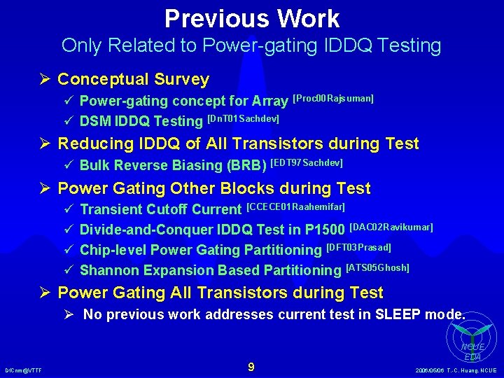
Previous Work Only Related to Power-gating IDDQ Testing Ø Conceptual Survey ü Power-gating concept for Array [Proc 00 Rajsuman] ü DSM IDDQ Testing [Dn. T 01 Sachdev] Ø Reducing IDDQ of All Transistors during Test ü Bulk Reverse Biasing (BRB) [EDT 97 Sachdev] Ø Power Gating Other Blocks during Test ü ü Transient Cutoff Current [CCECE 01 Raahemifar] Divide-and-Conquer IDDQ Test in P 1500 [DAC 02 Ravikumar] Chip-level Power Gating Partitioning [DFT 03 Prasad] Shannon Expansion Based Partitioning [ATS 05 Ghosh] Ø Power Gating All Transistors during Test Ø No previous work addresses current test in SLEEP mode. Df. Cnm@VTTF 9 NCUE EDA 2006/05/06 T. -C. Huang, NCUE
![Transient Cutoff Current CCECE 01 Raahemifar Ø Pattern residue enables the latch Ø However Transient Cutoff Current [CCECE 01 Raahemifar] Ø Pattern residue enables the latch Ø However,](https://slidetodoc.com/presentation_image_h2/8fb186da3d436af75a7b350878206a2e/image-10.jpg)
Transient Cutoff Current [CCECE 01 Raahemifar] Ø Pattern residue enables the latch Ø However, most nodes are easily pulled up and the remaining bridging current is weak. NCUE Df. Cnm@VTTF 10 EDA 2006/05/06 T. -C. Huang, NCUE
![Core IDDQ Test in P 1500 DAC 02 Ravikumar Ø Leakage current is divided Core IDDQ Test in P 1500 [DAC 02 Ravikumar] Ø Leakage current is divided.](https://slidetodoc.com/presentation_image_h2/8fb186da3d436af75a7b350878206a2e/image-11.jpg)
Core IDDQ Test in P 1500 [DAC 02 Ravikumar] Ø Leakage current is divided. Ø However, O(n) test time increases and intercore bridges cannot be tested. Df. Cnm@VTTF 11 NCUE EDA 2006/05/06 T. -C. Huang, NCUE
![Shannon Expansion ATS 05 Ghosh Ø Adaptively partitioned by input pattern xi Ø Area Shannon Expansion [ATS 05 Ghosh] Ø Adaptively partitioned by input pattern xi. Ø Area](https://slidetodoc.com/presentation_image_h2/8fb186da3d436af75a7b350878206a2e/image-12.jpg)
Shannon Expansion [ATS 05 Ghosh] Ø Adaptively partitioned by input pattern xi. Ø Area overhead, performance impact, serious stack impact and limited improvement. Df. Cnm@VTTF 12 NCUE EDA 2006/05/06 T. -C. Huang, NCUE

Outline Ø Introduction ü Issue of IDDQ Test in NMT ü Leakage Analysis Ø Previous Work Ø Technological Background Ø Proposed Scheme and Design for IDDS Testing ü Basic Concept and Basic Structure ü Inter-gate IDDS Testing ü Intra-gate IDDS Testing Ø Experimental Results Ø Conclusions Df. Cnm@VTTF 13 NCUE EDA 2006/05/06 T. -C. Huang, NCUE

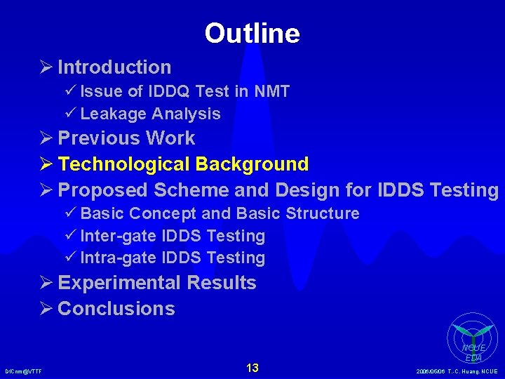
Key Points to IDDS Testing Ø Supper Cutoff ü Minimize leakages of non-defective circuit during test ü Some guy would like to pay or share the area cost ü Bridging paths won’t be cut off by supply switches Ø Data Retention ü Capability to propagate test pattern in normal mode ü Capability to keep data to stimulate bridging faults Ø Current-Path Differentiable ü i-path/v-path mapping [CCECE 01 Raahemifar] ü Keeping response for later observation Df. Cnm@VTTF 14 NCUE EDA 2006/05/06 T. -C. Huang, NCUE

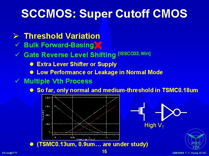
SCCMOS: Super Cutoff CMOS Ø Threshold Variation ü Bulk Forward-Basing ü Gate Reverse Level Shifting [ISSCC 03, Min] l Extra Lever Shifter or Supply l Low Performance or Leakage in Normal Mode ü Multiple Vth Process l So far, only normal and medium-threshold in TSMC 0. 18 um High VT l (TSMC 0. 13 um, 0. 9 um… are under study) Df. Cnm@VTTF 15 NCUE EDA 2006/05/06 T. -C. Huang, NCUE
![OnOff Current Ratio Ø IonIoff trades delay cost with leakage reduction ISCA 02 Heo On/Off Current Ratio Ø Ion/Ioff trades delay cost with leakage reduction [ISCA 02 Heo]](https://slidetodoc.com/presentation_image_h2/8fb186da3d436af75a7b350878206a2e/image-16.jpg)
On/Off Current Ratio Ø Ion/Ioff trades delay cost with leakage reduction [ISCA 02 Heo] Df. Cnm@VTTF 16 NCUE EDA 2006/05/06 T. -C. Huang, NCUE

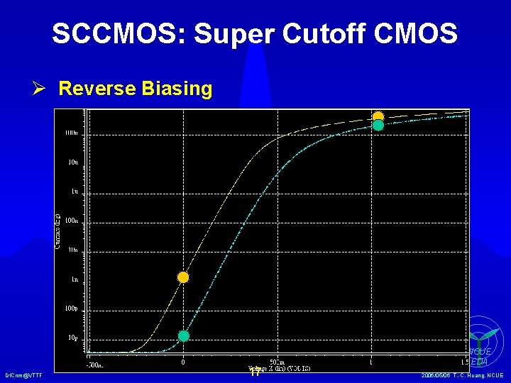
SCCMOS: Super Cutoff CMOS Ø Reverse Biasing Df. Cnm@VTTF 17 NCUE EDA 2006/05/06 T. -C. Huang, NCUE

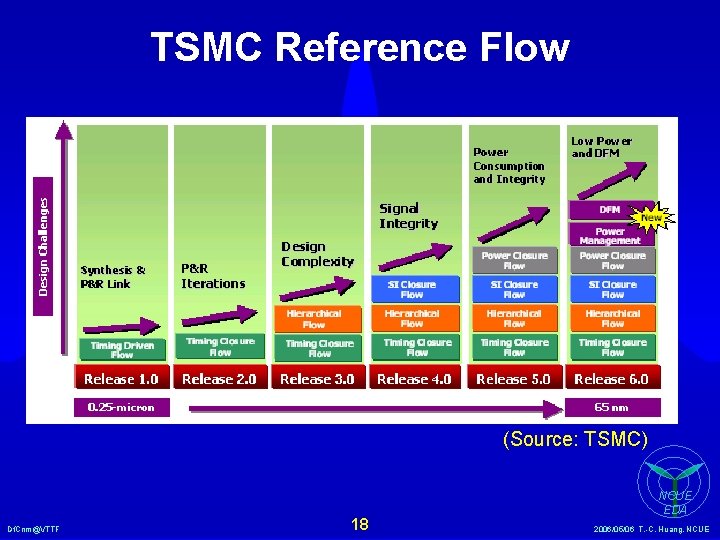
TSMC Reference Flow (Source: TSMC) Df. Cnm@VTTF 18 NCUE EDA 2006/05/06 T. -C. Huang, NCUE

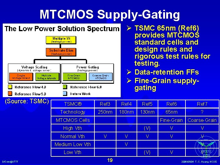
MTCMOS Supply-Gating Ø TSMC 65 nm (Ref 6) provides MTCMOS standard cells and design rules and rigorous test rules for testing. Ø Data-retention FFs Ø Fine-Grain supplygating (Source: TSMC) TSMC® Ref 3 Ref 4 Ref 5 Ref 6 Ref 7 Technology 250 nm 180 nm 130 nm 65 nm ? MTCMOS Cells Fine-Grain Coarse-Grain High Vth Normal Vth V V Medium Low Vth V V V Low Vth Df. Cnm@VTTF (V) V (V) 19 V NCUE V EDA 2006/05/06 T. -C. Huang, NCUE

Outline Ø Introduction ü Issue of IDDQ Test in NMT ü Leakage Analysis Ø Previous Work Ø Technological Background Ø Proposed Scheme and Design for IDDS Testing ü Basic Concept and Basic Structure ü Inter-gate IDDS Testing ü Intra-gate IDDS Testing Ø Experimental Results Ø Conclusions Df. Cnm@VTTF 20 NCUE EDA 2006/05/06 T. -C. Huang, NCUE
![Basic Structure VLSIDAT 06 SupplyGating for Data Retention Spike Reduction VDD Sp Ø Basic Structure: [VLSI-DAT 06] Supply-Gating for Data Retention & Spike Reduction VDD Sp Ø](https://slidetodoc.com/presentation_image_h2/8fb186da3d436af75a7b350878206a2e/image-21.jpg)
Basic Structure: [VLSI-DAT 06] Supply-Gating for Data Retention & Spike Reduction VDD Sp Ø Balanced Header In Out ü Equal Noise Margin ü Equal Rise/Fall Time 1 0 Ø Data Retention Wk SLEEP Df. Cnm@VTTF Footer ü Sudden Management ü Promising Df. CT Sp Wk 21 NCUE EDA 2006/05/06 T. -C. Huang, NCUE

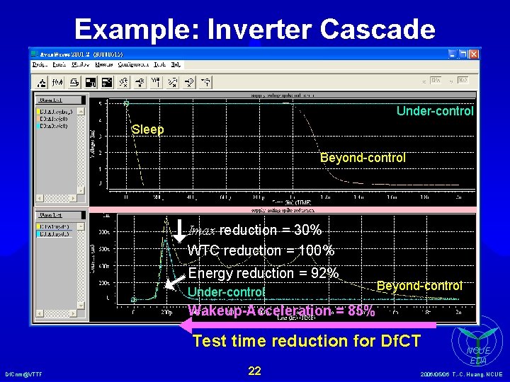
Example: Inverter Cascade Under-control Sleep Beyond-control Imax reduction = 30% WTC reduction = 100% Energy reduction = 92% Under-control Beyond-control Wakeup-Acceleration = 85% Test time reduction for Df. CT Df. Cnm@VTTF 22 NCUE EDA 2006/05/06 T. -C. Huang, NCUE

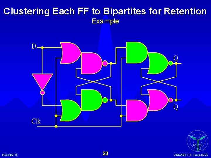
Clustering Each FF to Bipartites for Retention Example Df. Cnm@VTTF 23 NCUE EDA 2006/05/06 T. -C. Huang, NCUE

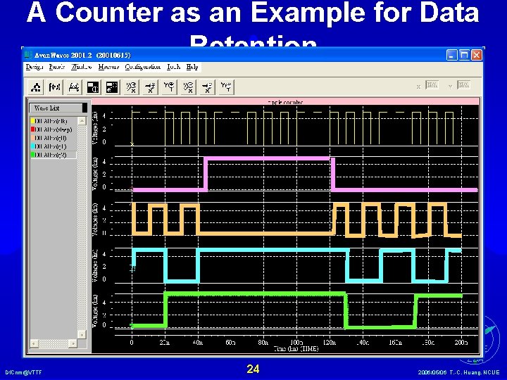
A Counter as an Example for Data Retention Df. Cnm@VTTF 24 NCUE EDA 2006/05/06 T. -C. Huang, NCUE

Outline Ø Introduction ü Issue of IDDQ Test in NMT ü Leakage Analysis Ø Previous Work Ø Technological Background Ø Proposed Scheme and Design for IDDS Testing ü Basic Concept and Basic Structure ü Inter-gate IDDS Testing ü Intra-gate IDDS Testing Ø Experimental Results Ø Conclusions Df. Cnm@VTTF 25 NCUE EDA 2006/05/06 T. -C. Huang, NCUE

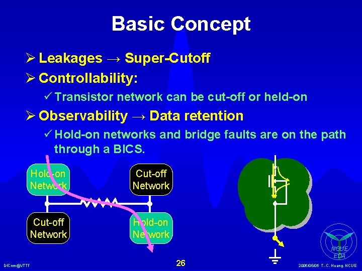
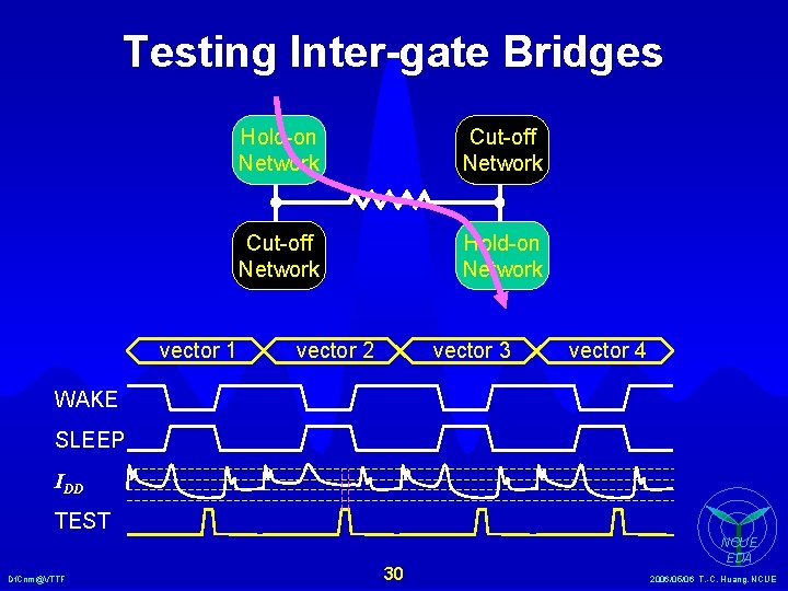
Basic Concept Ø Leakages → Super-Cutoff Ø Controllability: ü Transistor network can be cut-off or held-on Ø Observability → Data retention ü Hold-on networks and bridge faults are on the path through a BICS. Hold-on Network Cut-off Network Hold-on Network Df. Cnm@VTTF 26 NCUE EDA 2006/05/06 T. -C. Huang, NCUE

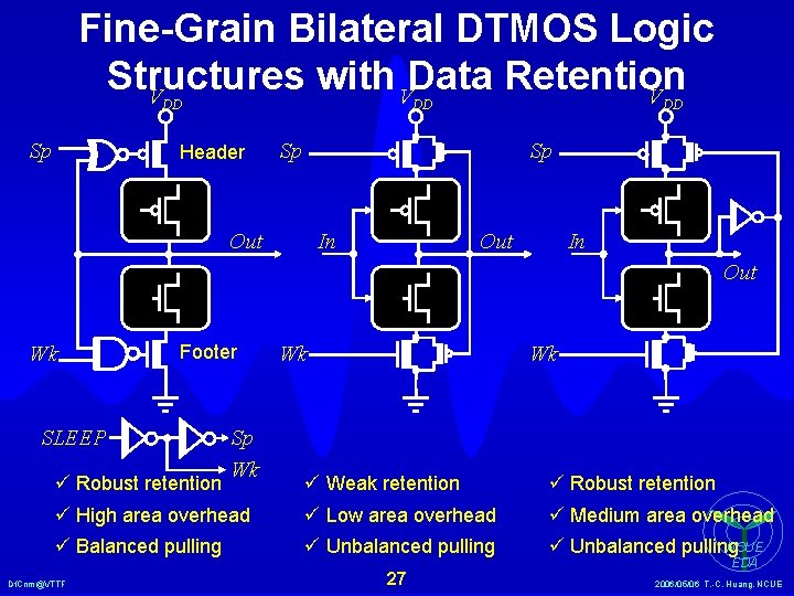
Fine-Grain Bilateral DTMOS Logic Structures with VData Retention V V DD Sp DD Header DD Sp Sp Out In In Out Wk Footer SLEEP ü Robust retention Sp Wk Wk Wk ü Weak retention ü Robust retention ü High area overhead ü Low area overhead ü Medium area overhead ü Balanced pulling ü Unbalanced pulling NCUE ü Unbalanced pulling Df. Cnm@VTTF 27 EDA 2006/05/06 T. -C. Huang, NCUE

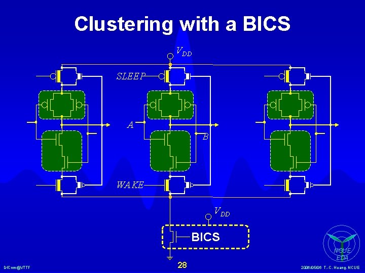
Clustering with a BICS VDD SLEEP A B WAKE VDD BICS Df. Cnm@VTTF 28 NCUE EDA 2006/05/06 T. -C. Huang, NCUE

Outline Ø Introduction ü Issue of IDDQ Test in NMT ü Leakage Analysis Ø Previous Work Ø Technological Background Ø Proposed Scheme and Design for IDDS Testing ü Basic Concept and Basic Structure ü Inter-gate IDDS Testing ü Intra-gate IDDS Testing Ø Experimental Results Ø Conclusions Df. Cnm@VTTF 29 NCUE EDA 2006/05/06 T. -C. Huang, NCUE

Testing Inter-gate Bridges vector 1 Hold-on Network Cut-off Network Hold-on Network vector 2 vector 3 vector 4 WAKE SLEEP IDD TEST Df. Cnm@VTTF 30 NCUE EDA 2006/05/06 T. -C. Huang, NCUE

Pattern Generation Ø Inter-gate 1. Two terminals of the bridge are justified to opposite values. 2. Different from IDDQ Testing, both 01 and 10 should be stimulated at the two terminals. 3. PODEM-like Algorithm. 4. Efficient collapsing. Df. Cnm@VTTF 31 NCUE EDA 2006/05/06 T. -C. Huang, NCUE

Outline Ø Introduction ü Issue of IDDQ Test in NMT ü Leakage Analysis Ø Previous Work Ø Technological Background Ø Proposed Scheme and Design for IDDS Testing ü Basic Concept and Basic Structure ü Inter-gate IDDS Testing ü Intra-gate IDDS Testing Ø Experimental Results Ø Conclusions Df. Cnm@VTTF 32 NCUE EDA 2006/05/06 T. -C. Huang, NCUE

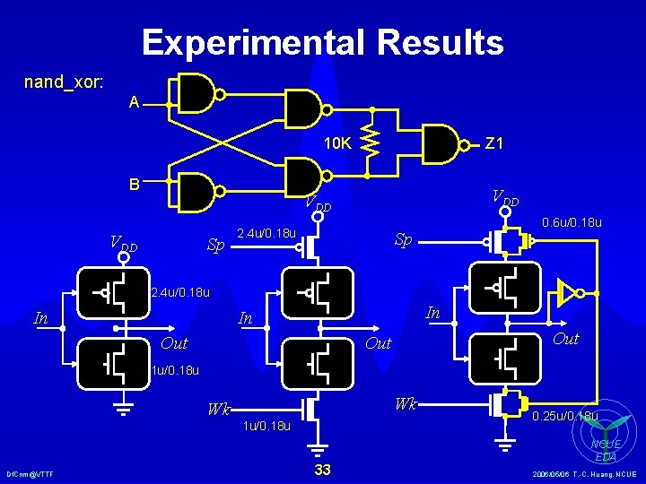
Experimental Results nand_xor: A 10 K B Z 1 VDD VDD Sp 2. 4 u/0. 18 u 0. 6 u/0. 18 u Sp 2. 4 u/0. 18 u In In In Out Out 1 u/0. 18 u Wk Df. Cnm@VTTF Wk 1 u/0. 18 u 33 0. 25 u/0. 18 u NCUE EDA 2006/05/06 T. -C. Huang, NCUE

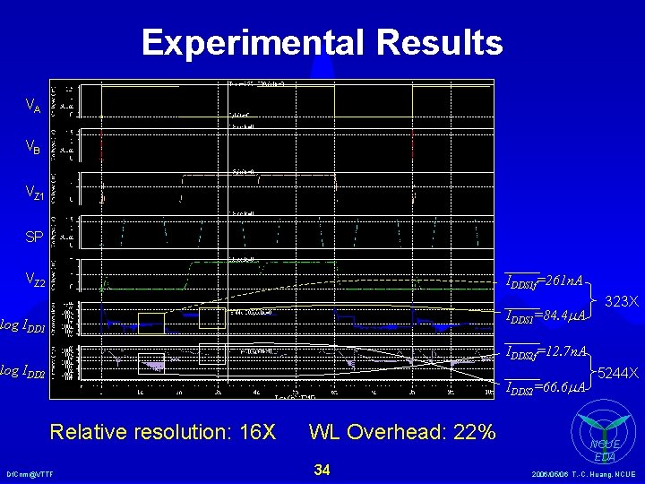
Experimental Results VA VB VZ 1 SP VZ 2 IDDS 1 f=261 n. A IDDS 1=84. 4 m. A log IDD 1 323 X IDDS 2 f=12. 7 n. A log IDD 2 IDDS 2=66. 6 m. A Relative resolution: 16 X Df. Cnm@VTTF WL Overhead: 22% 34 5244 X NCUE EDA 2006/05/06 T. -C. Huang, NCUE

Outline Ø Introduction ü Issue of IDDQ Test in NMT ü Leakage Analysis Ø Previous Work Ø Technological Background Ø Proposed Scheme and Design for IDDS Testing ü Basic Concept and Basic Structure ü Inter-gate IDDS Testing ü Intra-gate IDDS Testing Ø Experimental Results Ø Conclusions Df. Cnm@VTTF 35 NCUE EDA 2006/05/06 T. -C. Huang, NCUE

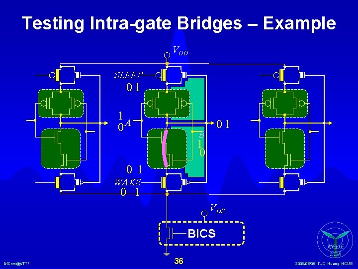
Testing Intra-gate Bridges – Example VDD SLEEP 01 1 0 A 01 B 1 0 0 1 WAKE 0 1 VDD BICS Df. Cnm@VTTF 36 NCUE EDA 2006/05/06 T. -C. Huang, NCUE

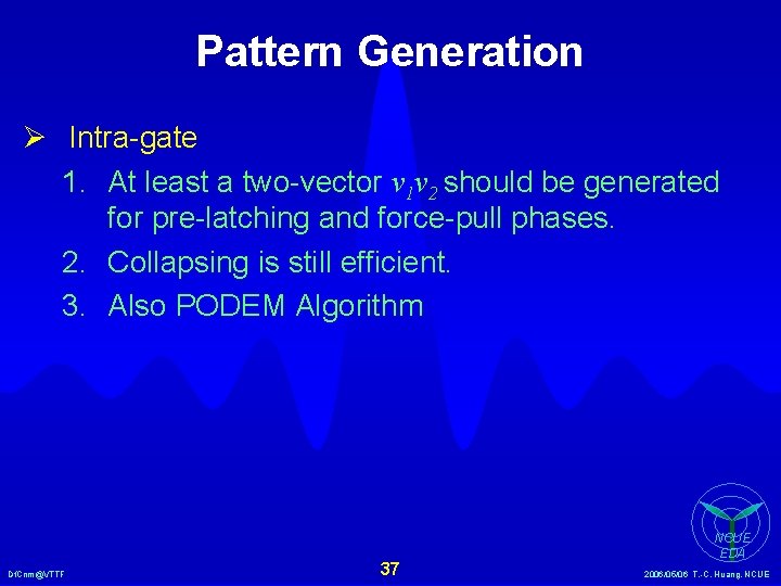
Pattern Generation Ø Intra-gate 1. At least a two-vector v 1 v 2 should be generated for pre-latching and force-pull phases. 2. Collapsing is still efficient. 3. Also PODEM Algorithm Df. Cnm@VTTF 37 NCUE EDA 2006/05/06 T. -C. Huang, NCUE

Outline Ø Introduction ü Issue of IDDQ Test in NMT ü Leakage Analysis Ø Previous Work Ø Technological Background Ø Proposed Scheme and Design for IDDS Testing ü Basic Concept and Basic Structure ü Inter-gate IDDS Testing ü Intra-gate IDDS Testing Ø Experimental Results Ø Conclusions Df. Cnm@VTTF 38 NCUE EDA 2006/05/06 T. -C. Huang, NCUE

Conclusions Ø A novel Df. CT for NMT is proposed. Ø Advantage: üHigh defect coverage using current test. Ø Disadvantage: üArea Overhead üPerformance Impact Df. Cnm@VTTF 39 NCUE EDA 2006/05/06 T. -C. Huang, NCUE

Future Work Ø Needs: üMTCMOS with Ioff. HT/Ion. HT>> Ioff. LT/Ion. LT is expected for IDDS testing in future technology. üDVDTMOS for IDDS will be developed. Ø Extension: üDomino, CVSL and Pseudo NMOS üIntegration of power management and Current Test Df. Cnm@VTTF 40 NCUE EDA 2006/05/06 T. -C. Huang, NCUE
![References 1 2 3 4 5 6 7 8 European Design and Test Conf References [1] [2] [3] [4] [5] [6] [7] [8] European Design and Test Conf.](https://slidetodoc.com/presentation_image_h2/8fb186da3d436af75a7b350878206a2e/image-41.jpg)
References [1] [2] [3] [4] [5] [6] [7] [8] European Design and Test Conf. Pages 271 -278, 1997. R. Rajsuman. IDDQ Testing for CMOS VLSI. IEEE Proceedings, Volume 88, Issue 4, pages 544 -568, Sep. 2000. M. Sachdev. Current-based testing for deep-submicron VLSIs. IEEE Design & Test of Computers, vol. 18, issue. 2, pp. 76 -84, Mar. 2001. S. Ghosh, S. Bhunia and K. Roy. Shannon Expansion Based Supply-Gated Logic for Improved Power and Testability. Asian Test Symposium, pages 404409, 2005. K. Raahemifar and M. Ahmadi. Fault characterizations and design-fortestability technique for detecting IDDQ faults in CMOS/Bi. CMOS circuits. Canadian Conference on Electrical and Computer Engineering, v. 2, pp. 13 -16, May 2001. A. Prasad. Chip Level Power Supply Partitioning for IDDQ Testing using Built. In Current Sensors. Proc. 18 th IEEE International Symposium on Defect and Fault Tolerance in VLSI Systems, pp. 140 -143, 2003. C. P. Ravikumar and R. Kumar. Divide-and-conquer IDDQ testing for corebased system chips. Proc. 7 th Asia and South Pacific Design Automation Conference, pp. 761 -655, Jan. 2002. S. Heo, et. al. Dynamic Fine Grain Leakage Reduction using Leakage Biased NCUE Bitlines. Int’l Symp. on Computer Architecture, Pp. 137 -147, 2002. EDA Df. Cnm@VTTF 41 2006/05/06 T. -C. Huang, NCUE