VLSI Design TsungChu Huang Department of Electronic Engineering
- Slides: 81

VLSI Design Tsung-Chu Huang Department of Electronic Engineering National Changhua University of Education Email: tch@cc. ncue. edu. tw 2015/09/14 TCH T. -C. Huang, NCUE Fall 2015 NCUE Page 1

Brief Syllabus 1. Visit http: //testlab. ncue. edu. tw/tch for details 2. Reference: Weste & Harris’s textbook 3. All-English Instruction 4. Requirements for This Course: ü Basic Logic Design ü Hardware Descriptive Language ü Self-Motivation 5. Addendum: TCH ü ftp: //testlab. ncue. edu. tw/VLSI T. -C. Huang, NCUE Fall 2015 NCUE Page 2

Course Scope 1. Scoped in CMOS with 80% Digital + 20% Else 2. Why Go CMOS: 1. 2. 3. 4. 5. 6. 7. Low power/cost High density High Noise Margin High Regularization Ratioless Circuits Compromised for Analog Design Highly Developed. 3. Why Digital First: 1. High digitalization except AD/DA and a part of PLL TCH 2. Easy to start up NCUE T. -C. Huang, NCUE Fall 2015 Page 3

Major Contents 1. Logic-Oriented MOS Theory – Transistor Sizing 2. Logic Cells – Full-custom Layout 3. Digital IC Synthesis – Cell-base Layout 4. Logic Structures and RTL Modules 5. Introduction to Digital IP 6. Introduction to Memory Design 7. Introduction to Logic Testing 8. Introduction to Some Basics for Analog Circuits 9. Introduction to SOC Design TCH T. -C. Huang, NCUE Fall 2015 NCUE Page 4

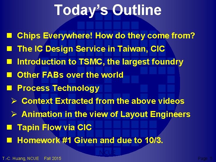
Today’s Outline n Chips Everywhere! How do they come from? n The IC Design Service in Taiwan, CIC n Introduction to TSMC, the largest foundry n Other FABs over the world n Process Technology Ø Context Extracted from the above videos Ø Animation in the view of Layout Engineers n Tapin Flow via CIC n Homework #1 Given and due to 10/3. TCH T. -C. Huang, NCUE Fall 2015 NCUE Page 5

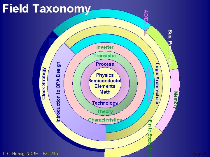
Inverter Theory Characteristics TCH T. -C. Huang, NCUE Fall 2015 NCUE Finite State Mach Introduction to OPA Design Technology Memory Physics Semiconductor Elements Math Logic Architecture Process Logic Structures Clock Strategy Transistor Bus, Power Grid AD/DA, PLL Field Taxonomy Page 6

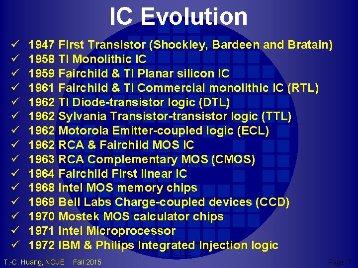
IC Evolution ü ü ü ü 1947 First Transistor (Shockley, Bardeen and Bratain) 1958 TI Monolithic IC 1959 Fairchild & TI Planar silicon IC 1961 Fairchild & TI Commercial monolithic IC (RTL) 1962 TI Diode-transistor logic (DTL) 1962 Sylvania Transistor-transistor logic (TTL) 1962 Motorola Emitter-coupled logic (ECL) 1962 RCA & Fairchild MOS IC 1963 RCA Complementary MOS (CMOS) 1964 Fairchild First linear IC 1968 Intel MOS memory chips 1969 Bell Labs Charge-coupled devices (CCD) 1970 Mostek MOS calculator chips 1971 Intel Microprocessor TCH 1972 IBM & Philips Integrated Injection logic T. -C. Huang, NCUE Fall 2015 NCUE Page 7

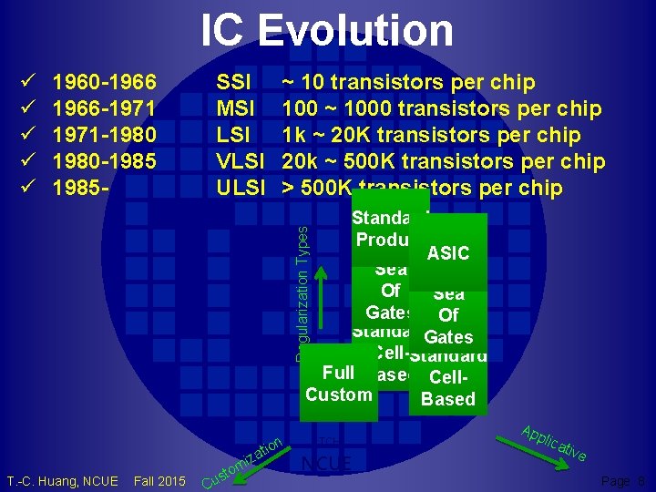
IC Evolution ü ü ü 1960 -1966 -1971 -1980 -1985 - SSI MSI LSI VLSI ULSI ~ 10 transistors per chip 100 ~ 1000 transistors per chip 1 k ~ 20 K transistors per chip 20 k ~ 500 K transistors per chip > 500 K transistors per chip Regularization Types Standard FPGA Product CPLD ASIC Sea Of Sea Gates Of Standard. Gates Semi. Cell-Standard Custom Full Based Cell. Custom Based T. -C. Huang, NCUE Fall 2015 C us t za i tom ion TCH NCUE Ap plic ativ e Page 8

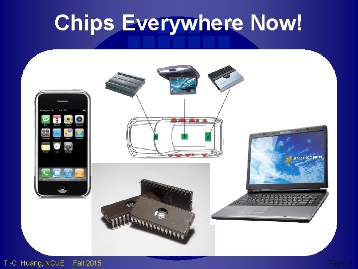
Chips Everywhere Now! TCH T. -C. Huang, NCUE Fall 2015 NCUE Page 9

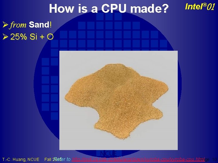
How is a CPU made? Intel® 01 Ø from Sand! Ø 25% Si + O TCH T. -C. Huang, NCUE Refer to http: //poli. cs. vsb. cz/edu/arp/down/vyroba-cpu. html Fall 2015 Page 10

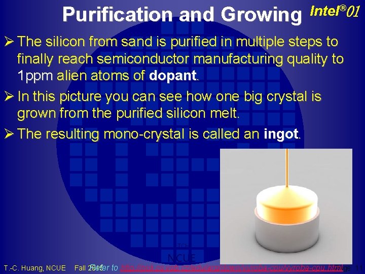
Purification and Growing Intel® 01 Ø The silicon from sand is purified in multiple steps to finally reach semiconductor manufacturing quality to 1 ppm alien atoms of dopant. Ø In this picture you can see how one big crystal is grown from the purified silicon melt. Ø The resulting mono-crystal is called an ingot. TCH T. -C. Huang, NCUE Refer to http: //poli. cs. vsb. cz/edu/arp/down/vyroba-cpu. html Fall 2015 Page 11

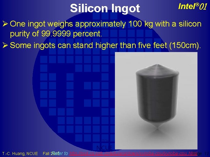
Silicon Ingot Intel® 01 Ø One ingot weighs approximately 100 kg with a silicon purity of 99. 9999 percent. Ø Some ingots can stand higher than five feet (150 cm). TCH T. -C. Huang, NCUE Refer to http: //poli. cs. vsb. cz/edu/arp/down/vyroba-cpu. html Fall 2015 Page 12

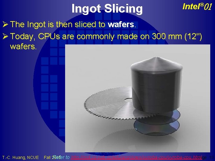
Ingot Slicing Intel® 01 Ø The Ingot is then sliced to wafers. Ø Today, CPUs are commonly made on 300 mm (12") wafers. TCH T. -C. Huang, NCUE Refer to http: //poli. cs. vsb. cz/edu/arp/down/vyroba-cpu. html Fall 2015 Page 13

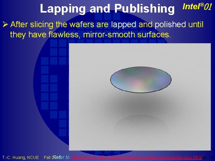
Lapping and Publishing Intel® 01 Ø After slicing the wafers are lapped and polished until they have flawless, mirror-smooth surfaces. TCH T. -C. Huang, NCUE Refer to http: //poli. cs. vsb. cz/edu/arp/down/vyroba-cpu. html Fall 2015 Page 14

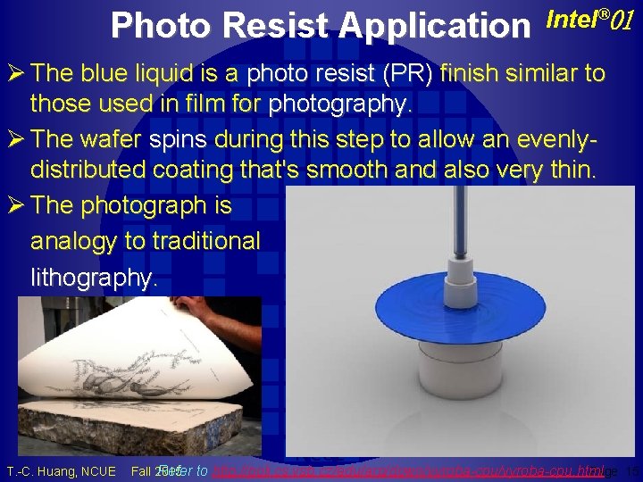
Photo Resist Application Intel® 01 Ø The blue liquid is a photo resist (PR) finish similar to those used in film for photography. Ø The wafer spins during this step to allow an evenlydistributed coating that's smooth and also very thin. Ø The photograph is analogy to traditional lithography. TCH T. -C. Huang, NCUE Refer to http: //poli. cs. vsb. cz/edu/arp/down/vyroba-cpu. html Fall 2015 Page 15

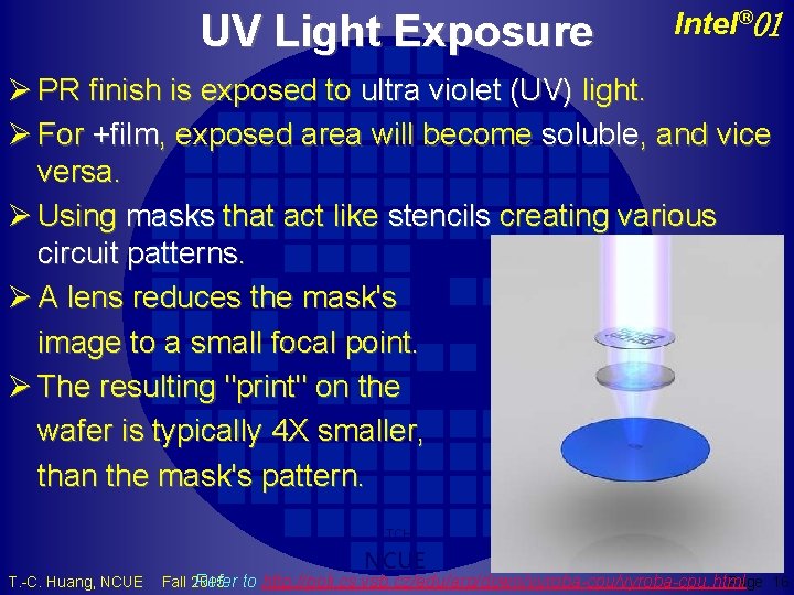
UV Light Exposure Intel® 01 Ø PR finish is exposed to ultra violet (UV) light. Ø For +film, exposed area will become soluble, and vice versa. Ø Using masks that act like stencils creating various circuit patterns. Ø A lens reduces the mask's image to a small focal point. Ø The resulting "print" on the wafer is typically 4 X smaller, than the mask's pattern. TCH T. -C. Huang, NCUE Refer to http: //poli. cs. vsb. cz/edu/arp/down/vyroba-cpu. html Fall 2015 Page 16

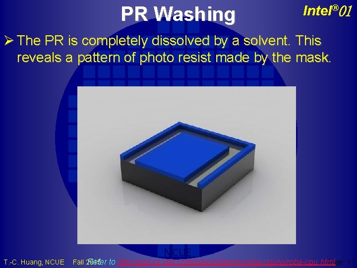
PR Washing Intel® 01 Ø The PR is completely dissolved by a solvent. This reveals a pattern of photo resist made by the mask. TCH T. -C. Huang, NCUE Refer to http: //poli. cs. vsb. cz/edu/arp/down/vyroba-cpu. html Fall 2015 Page 17

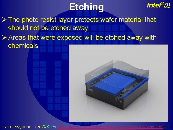
Etching Intel® 01 Ø The photo resist layer protects wafer material that should not be etched away. Ø Areas that were exposed will be etched away with chemicals. TCH T. -C. Huang, NCUE Refer to http: //poli. cs. vsb. cz/edu/arp/down/vyroba-cpu. html Fall 2015 Page 18

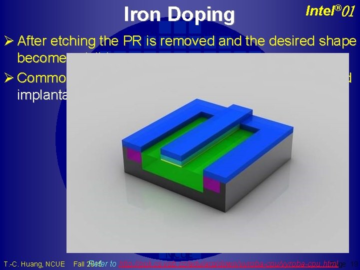
Iron Doping Intel® 01 Ø After etching the PR is removed and the desired shape becomes visible. Ø Common approaches for iron doping are diffusion and implantation. TCH T. -C. Huang, NCUE Refer to http: //poli. cs. vsb. cz/edu/arp/down/vyroba-cpu. html Fall 2015 Page 19

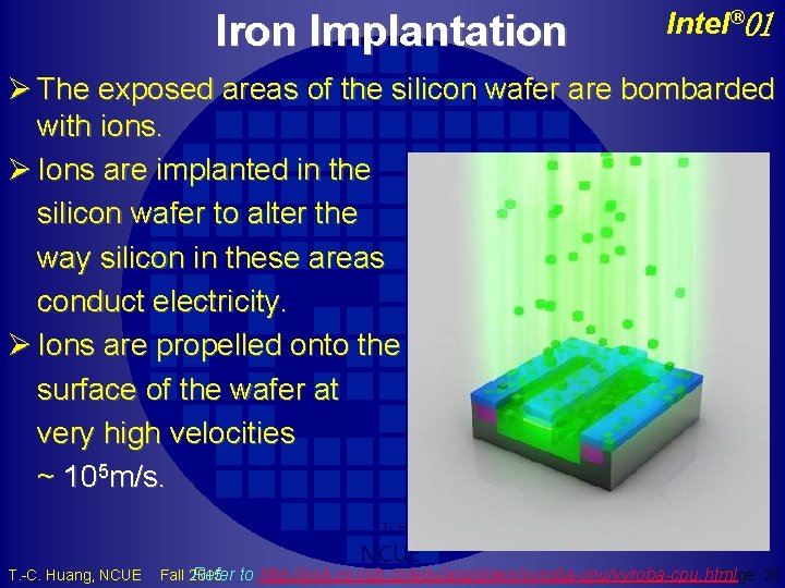
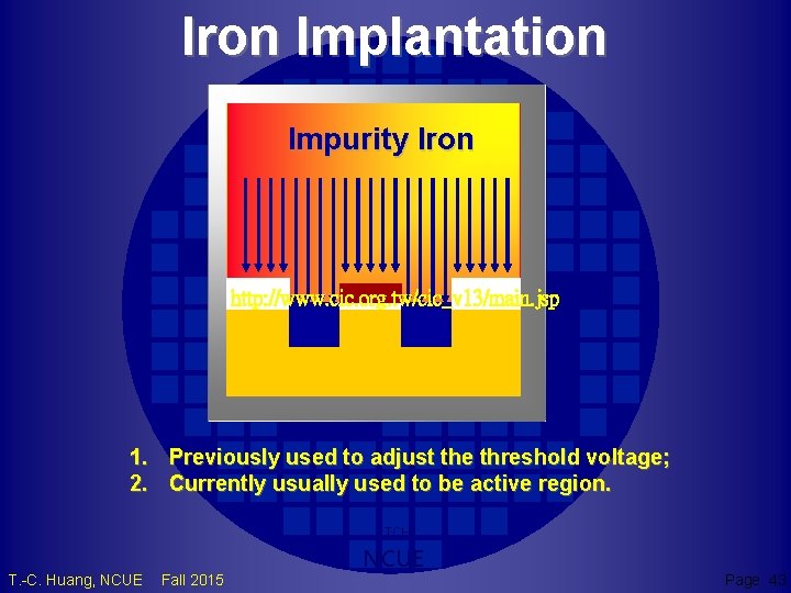
Iron Implantation Intel® 01 Ø The exposed areas of the silicon wafer are bombarded with ions. Ø Ions are implanted in the silicon wafer to alter the way silicon in these areas conduct electricity. Ø Ions are propelled onto the surface of the wafer at very high velocities ~ 105 m/s. TCH T. -C. Huang, NCUE Refer to http: //poli. cs. vsb. cz/edu/arp/down/vyroba-cpu. html Fall 2015 Page 20

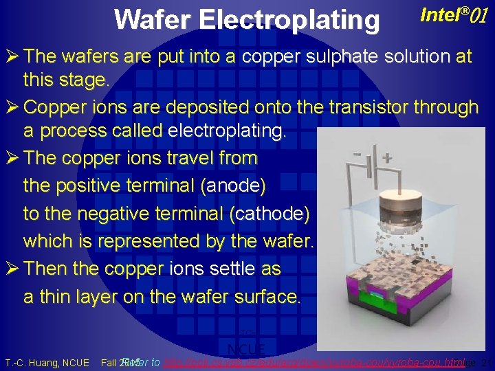
Wafer Electroplating Intel® 01 Ø The wafers are put into a copper sulphate solution at this stage. Ø Copper ions are deposited onto the transistor through a process called electroplating. Ø The copper ions travel from the positive terminal (anode) to the negative terminal (cathode) which is represented by the wafer. Ø Then the copper ions settle as a thin layer on the wafer surface. TCH T. -C. Huang, NCUE Refer to http: //poli. cs. vsb. cz/edu/arp/down/vyroba-cpu. html Fall 2015 Page 21

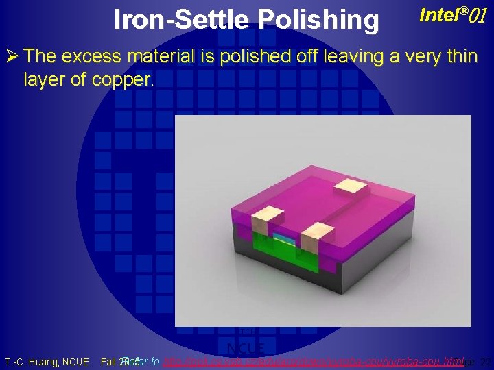
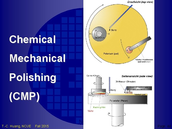
Iron-Settle Polishing Intel® 01 Ø The excess material is polished off leaving a very thin layer of copper. TCH T. -C. Huang, NCUE Refer to http: //poli. cs. vsb. cz/edu/arp/down/vyroba-cpu. html Fall 2015 Page 22

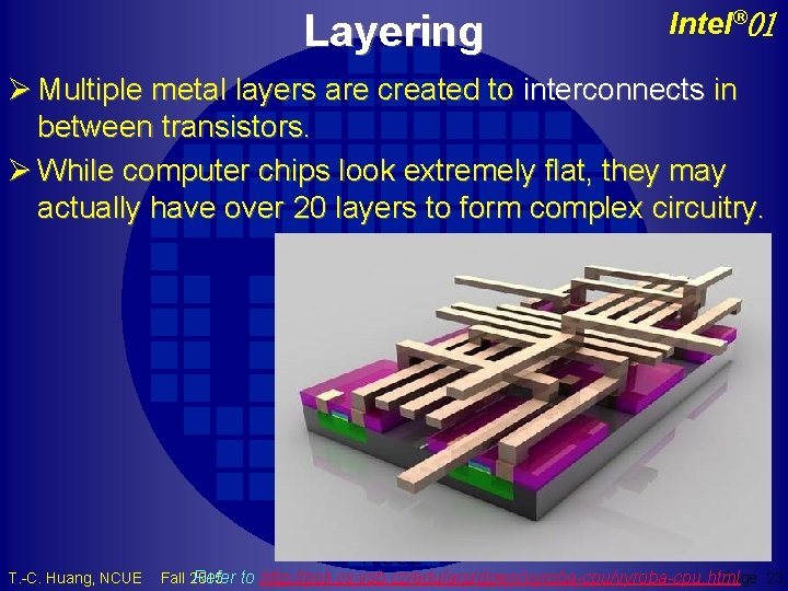
Layering Intel® 01 Ø Multiple metal layers are created to interconnects in between transistors. Ø While computer chips look extremely flat, they may actually have over 20 layers to form complex circuitry. TCH T. -C. Huang, NCUE Refer to http: //poli. cs. vsb. cz/edu/arp/down/vyroba-cpu. html Fall 2015 Page 23

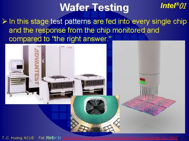
Wafer Testing Intel® 01 Ø In this stage test patterns are fed into every single chip and the response from the chip monitored and compared to "the right answer. " TCH T. -C. Huang, NCUE Refer to http: //poli. cs. vsb. cz/edu/arp/down/vyroba-cpu. html Fall 2015 Page 24

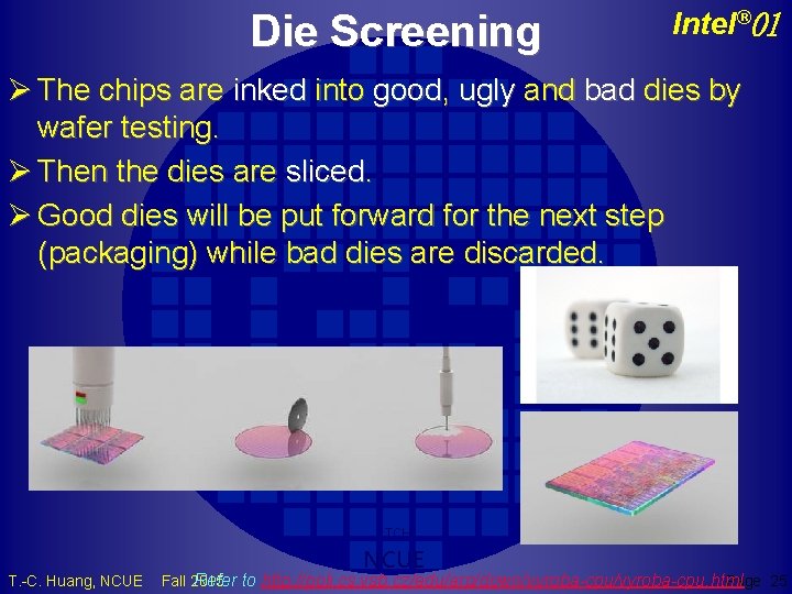
Die Screening Intel® 01 Ø The chips are inked into good, ugly and bad dies by wafer testing. Ø Then the dies are sliced. Ø Good dies will be put forward for the next step (packaging) while bad dies are discarded. TCH T. -C. Huang, NCUE Refer to http: //poli. cs. vsb. cz/edu/arp/down/vyroba-cpu. html Fall 2015 Page 25

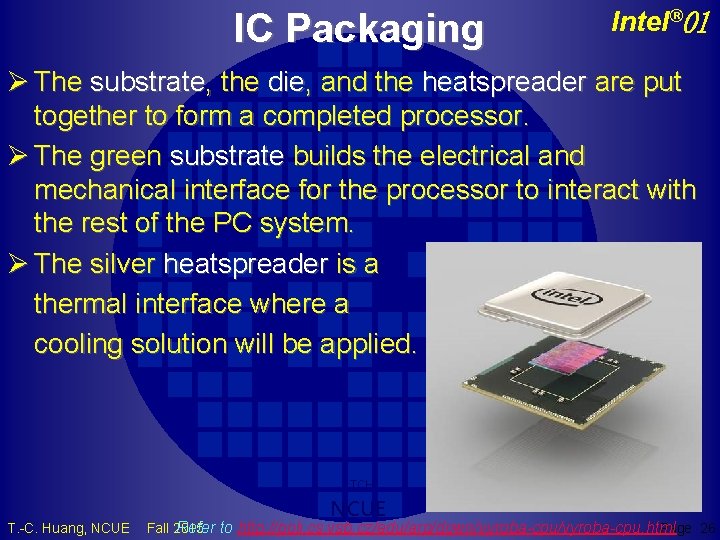
IC Packaging Intel® 01 Ø The substrate, the die, and the heatspreader are put together to form a completed processor. Ø The green substrate builds the electrical and mechanical interface for the processor to interact with the rest of the PC system. Ø The silver heatspreader is a thermal interface where a cooling solution will be applied. TCH T. -C. Huang, NCUE Refer to http: //poli. cs. vsb. cz/edu/arp/down/vyroba-cpu. html Fall 2015 Page 26

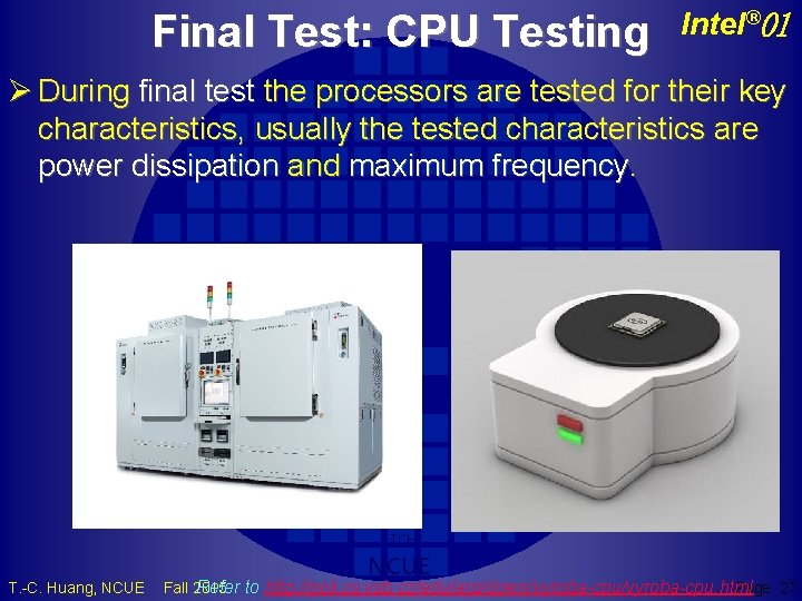
Final Test: CPU Testing Intel® 01 Ø During final test the processors are tested for their key characteristics, usually the tested characteristics are power dissipation and maximum frequency. TCH T. -C. Huang, NCUE Refer to http: //poli. cs. vsb. cz/edu/arp/down/vyroba-cpu. html Fall 2015 Page 27

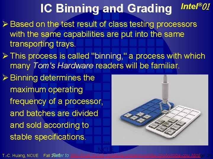
IC Binning and Grading Intel® 01 Ø Based on the test result of class testing processors with the same capabilities are put into the same transporting trays. Ø This process is called "binning, " a process with which many Tom's Hardware readers will be familiar. Ø Binning determines the maximum operating frequency of a processor, and batches are divided and sold according to stable specifications. TCH T. -C. Huang, NCUE Refer to http: //poli. cs. vsb. cz/edu/arp/down/vyroba-cpu. html Fall 2015 Page 28

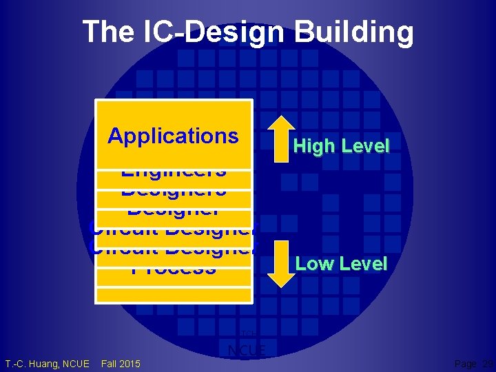
The IC-Design Building Applications Software System Engineers Architecture Designers Digital Designer Analogue Circuit Designer Semiconductor Circuit Designer Process Physics High Level Low Level TCH T. -C. Huang, NCUE Fall 2015 NCUE Page 29

Some Terminology Ø FAB: fabrication, analogy to layout-style manufacture Ø Foundry: factory for basing the industry chain like the metal castings, especially for semiconductor industry Ø FABless Design House: small design company usually w/o FAB equipments Ø CIC: Chip Implementation Center, National Applied Research Laboratories Ø MPW: Multi-Project Wafer TCH T. -C. Huang, NCUE Fall 2015 NCUE Page 30

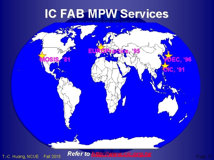
IC FAB MPW Services EUROPractice, ‘ 95 MOSIS, ‘ 81 VDEC, ‘ 96 CIC, ‘ 91 TCH T. -C. Huang, NCUE Fall 2015 NCUE Refer to http: //www. cic. org. tw Page 31

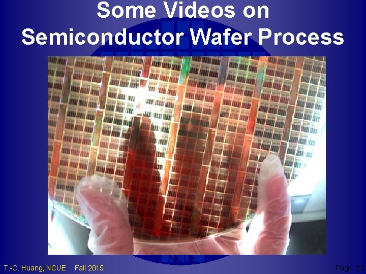
Some Videos on Semiconductor Wafer Process TCH T. -C. Huang, NCUE Fall 2015 NCUE Page 32

Videos on Silicon Wafer Processing Ø Wafer Process at Texas Instrument, 2000 (9 min) Ø Semiconductor Technology at TSMC, 2011 (8 min) Ø Chip Manufacture Process, 2008 (10 min) Ø CPU Manufacture at AMD, 2009 (11 min) Ø Intel 22 nm Fin. FET Process Flow, 2013 (10 min) TCH T. -C. Huang, NCUE Fall 2015 NCUE Page 33

Context Reviews on Process Tech 1. Si Semiconductor Technology 2. Basic CMOS Technology 3. CMOS Process 4. Layout Design Rules 5. Latchup Effect 6. Extractor & DRC 7. An n-Well CMOS Process Flow 8. CIC Tape-In Flow & Tutorial TCH T. -C. Huang, NCUE Fall 2015 NCUE Page 34

CMOS Process Tech 1. Oxidation (氧化) 2. Epitaxy (磊晶) 3. Deposition (沉積) 4. Implantation (植入) 5. Diffusion (擴散) TCH T. -C. Huang, NCUE Fall 2015 NCUE Page 35

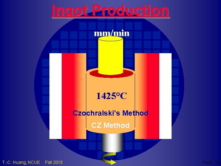
Ingot Production mm/min 1425°C Czochralski’s Method CZ Method TCH T. -C. Huang, NCUE Fall 2015 NCUE Page 36

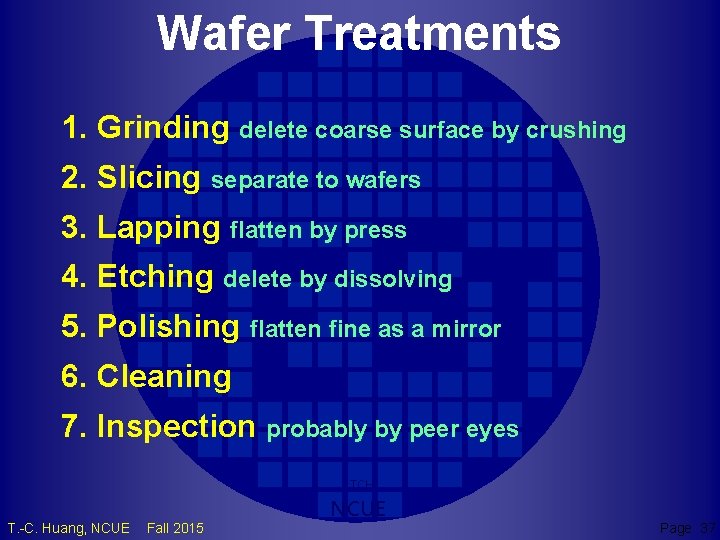
Wafer Treatments 1. Grinding delete coarse surface by crushing 2. Slicing separate to wafers 3. Lapping flatten by press 4. Etching delete by dissolving 5. Polishing flatten fine as a mirror 6. Cleaning 7. Inspection probably by peer eyes TCH T. -C. Huang, NCUE Fall 2015 NCUE Page 37

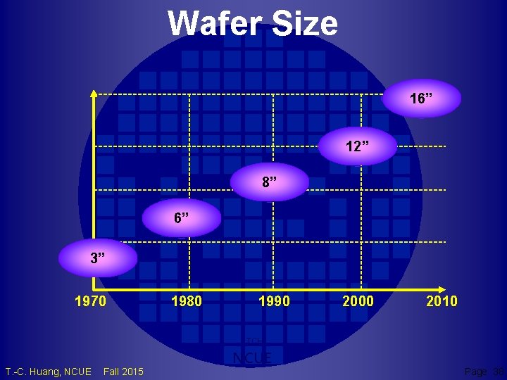
Wafer Size 16” 12” 8” 6” 3” 1970 1980 1990 2000 2010 TCH T. -C. Huang, NCUE Fall 2015 NCUE Page 38

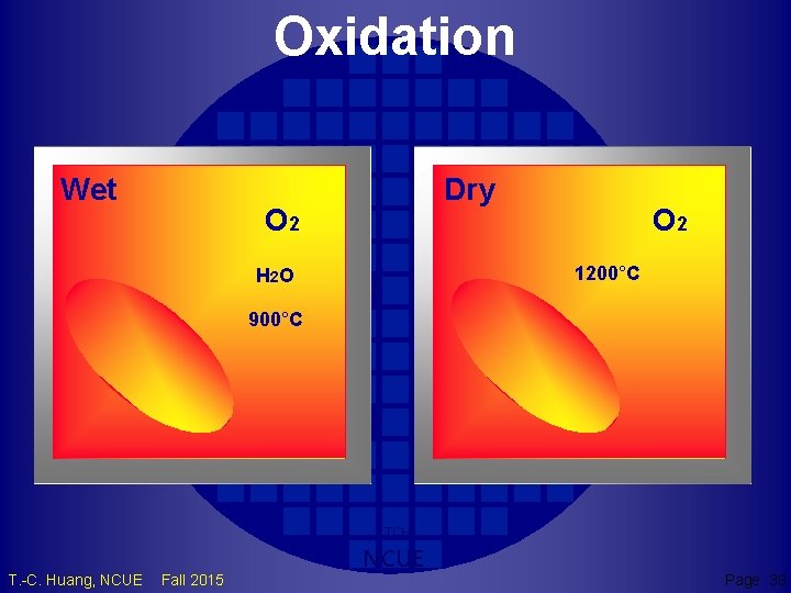
Oxidation Wet Dry O 2 1200°C H 2 O 900°C TCH T. -C. Huang, NCUE Fall 2015 NCUE Page 39

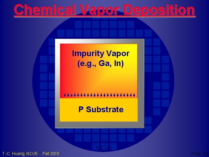
Chemical Vapor Deposition Impurity Vapor (e. g. , Ga, In) P Substrate TCH T. -C. Huang, NCUE Fall 2015 NCUE Page 40

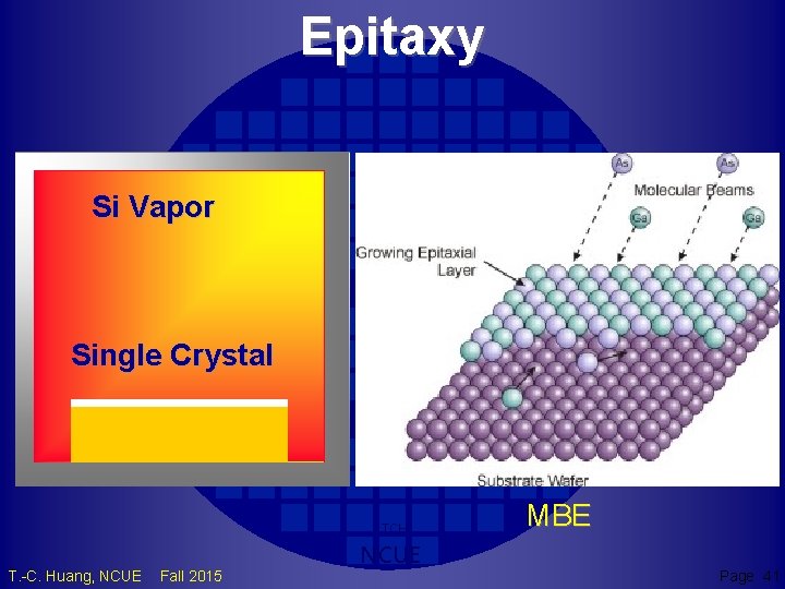
Epitaxy Si Vapor Single Crystal TCH T. -C. Huang, NCUE Fall 2015 NCUE MBE Page 41

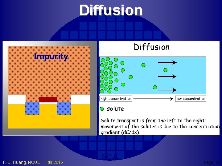
Diffusion Impurity TCH T. -C. Huang, NCUE Fall 2015 NCUE Page 42

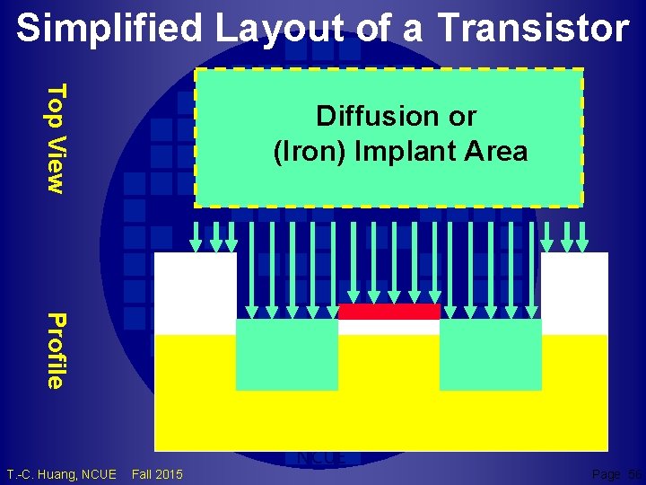
Iron Implantation Impurity Iron http: //www. cic. org. tw/cic_v 13/main. jsp 1. 2. Previously used to adjust the threshold voltage; Currently usually used to be active region. TCH T. -C. Huang, NCUE Fall 2015 NCUE Page 43

Chemical Mechanical Polishing (CMP) TCH T. -C. Huang, NCUE Fall 2015 NCUE Page 44

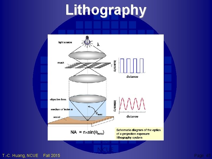
Lithography TCH T. -C. Huang, NCUE Fall 2015 NCUE Page 45

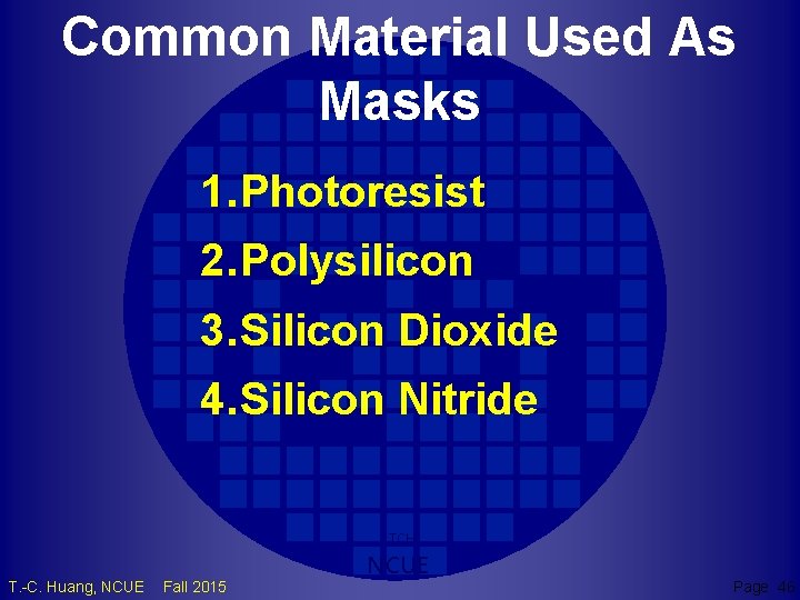
Common Material Used As Masks 1. Photoresist 2. Polysilicon 3. Silicon Dioxide 4. Silicon Nitride TCH T. -C. Huang, NCUE Fall 2015 NCUE Page 46

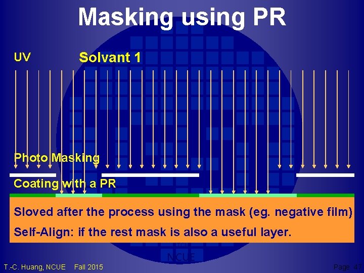
Masking using PR UV Solvant 1 Photo Masking Coating with a PR Sloved after the process using the mask (eg. negative film) Self-Align: if the rest mask is also a useful layer. TCH T. -C. Huang, NCUE Fall 2015 NCUE Page 47

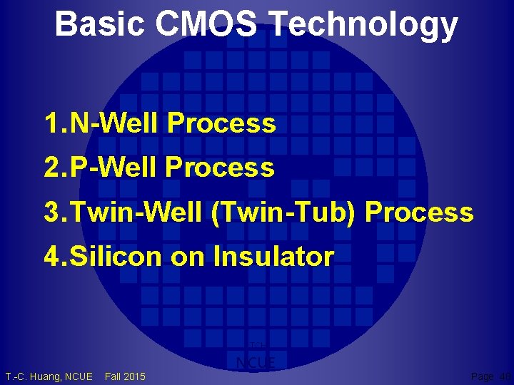
Basic CMOS Technology 1. N-Well Process 2. P-Well Process 3. Twin-Well (Twin-Tub) Process 4. Silicon on Insulator TCH T. -C. Huang, NCUE Fall 2015 NCUE Page 48

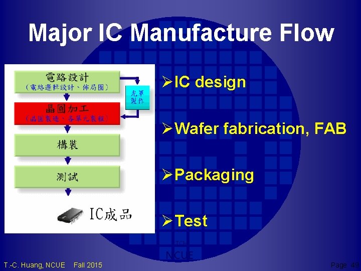
Major IC Manufacture Flow ØIC design ØWafer fabrication, FAB ØPackaging ØTest TCH T. -C. Huang, NCUE Fall 2015 NCUE Page 49

A Detailed MOS Process TCH NCUE Courtesy of Chuang, “VLSI Technology, ” ISBN: 957 -584 -327 -4. T. -C. Huang, NCUE Fall 2015 Page 50

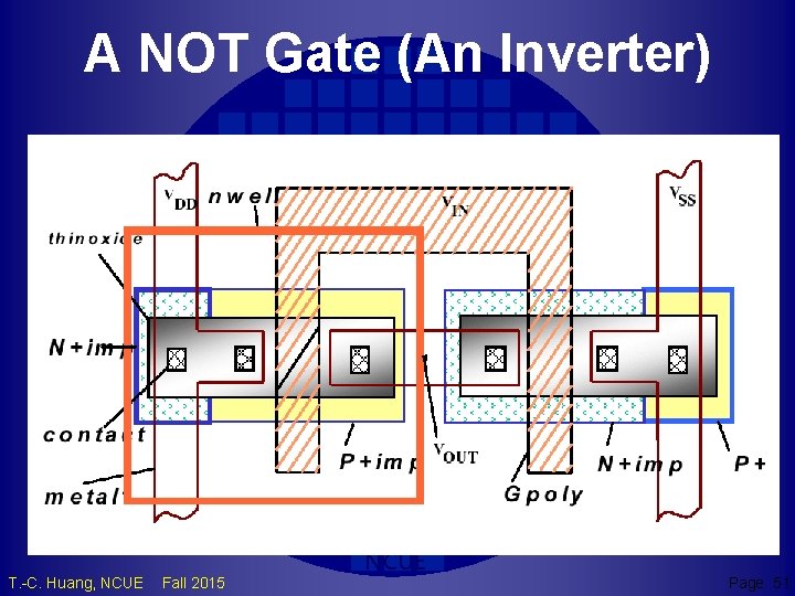
A NOT Gate (An Inverter) TCH T. -C. Huang, NCUE Fall 2015 NCUE Page 51

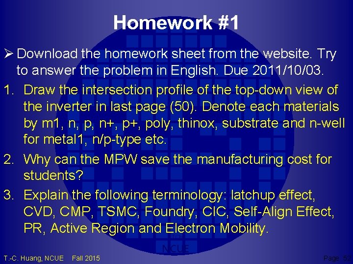
Homework #1 Ø Download the homework sheet from the website. Try to answer the problem in English. Due 2011/10/03. 1. Draw the intersection profile of the top-down view of the inverter in last page (50). Denote each materials by m 1, n, p, n+, poly, thinox, substrate and n-well for metal 1, n/p-type etc. 2. Why can the MPW save the manufacturing cost for students? 3. Explain the following terminology: latchup effect, CVD, CMP, TSMC, Foundry, CIC, Self-Align Effect, PR, Active Region and Electron Mobility. TCH T. -C. Huang, NCUE Fall 2015 NCUE Page 52

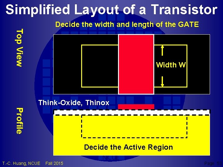
Simplified Layout of a Transistor Top View Decide the width and length of the GATE 長 L Width W Think-Oxide, Thinox Profile Decide TCH the Active Region T. -C. Huang, NCUE Fall 2015 NCUE Page 53

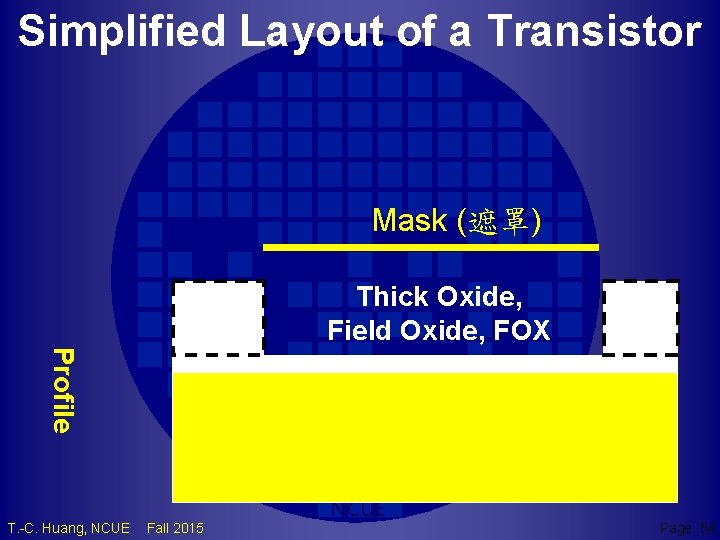
Simplified Layout of a Transistor Mask (遮罩) Thick Oxide, Field Oxide, FOX Profile TCH T. -C. Huang, NCUE Fall 2015 NCUE Page 54

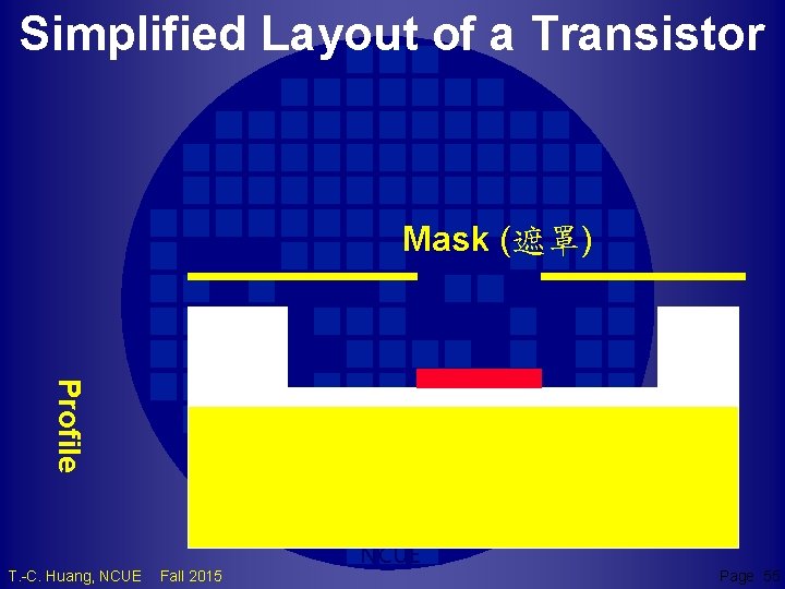
Simplified Layout of a Transistor Mask (遮罩) Profile TCH T. -C. Huang, NCUE Fall 2015 NCUE Page 55

Simplified Layout of a Transistor Top View Diffusion or (Iron) Implant Area Profile TCH T. -C. Huang, NCUE Fall 2015 NCUE Page 56

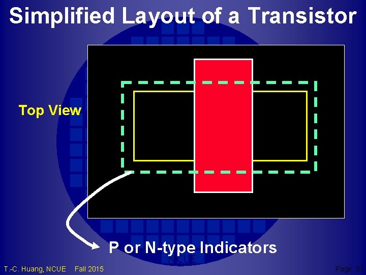
Simplified Layout of a Transistor Top View P or N-type Indicators TCH T. -C. Huang, NCUE Fall 2015 NCUE Page 57

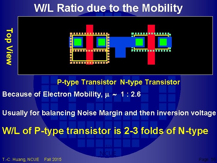
W/L Ratio due to the Mobility Top View P-type Transistor N-type Transistor Because of Electron Mobility, m ~ 1 : 2. 6 Usually for balancing Noise Margin and then inversion voltage W/L of P-type transistor is 2 -3 folds of N-type TCH T. -C. Huang, NCUE Fall 2015 NCUE Page 58

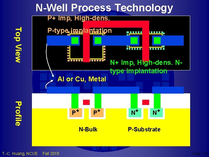
N-Well Process Technology P+ Imp, High-dens. Top View P-type implantation N+ Imp, High-dens. Ntype implantation Al or Cu, Metal Profile P+ P+ N+ N-Bulk N+ P-Substrate TCH T. -C. Huang, NCUE Fall 2015 NCUE Page 59

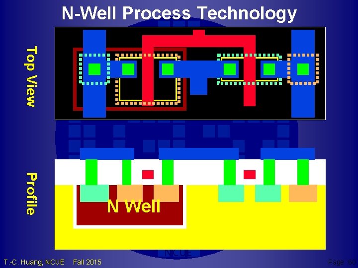
N-Well Process Technology Top View Profile N Well TCH T. -C. Huang, NCUE Fall 2015 NCUE Page 60

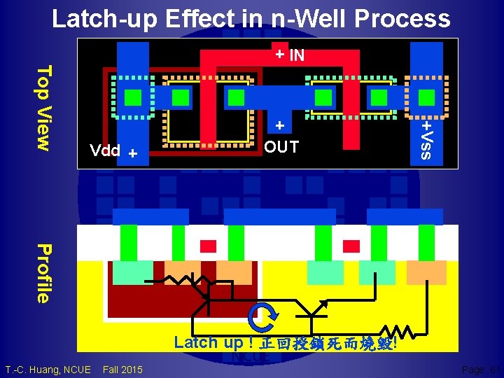
Latch-up Effect in n-Well Process Vdd OUT Vss Top View IN Profile Latch up TCH ! 正回授鎖死而燒毀! T. -C. Huang, NCUE Fall 2015 NCUE Page 61

Preventing Latch-up 1. Using Twin-Well 2. Evolved in DRC • Connect N/P-well to Vdd/Vss • Contacts closer to Source-gate • More contacts for more transistors • Sometimes one well contact for a transistor. TCH T. -C. Huang, NCUE Fall 2015 NCUE Page 62

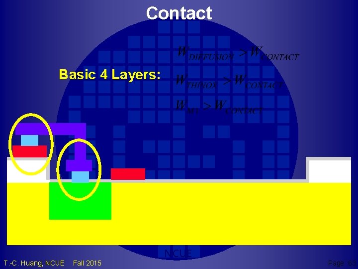
Contact Basic 4 Layers: TCH T. -C. Huang, NCUE Fall 2015 NCUE Page 63

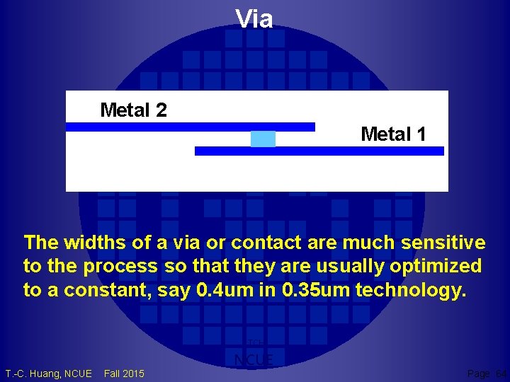
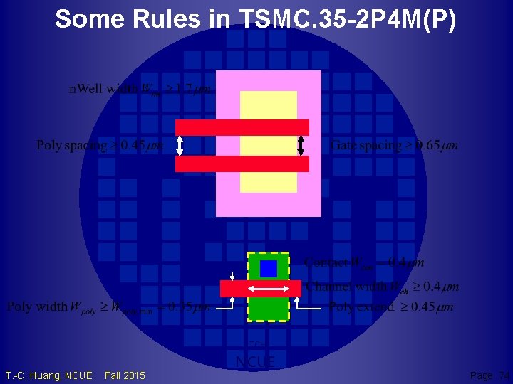
Via Metal 2 Metal 1 The widths of a via or contact are much sensitive to the process so that they are usually optimized to a constant, say 0. 4 um in 0. 35 um technology. TCH T. -C. Huang, NCUE Fall 2015 NCUE Page 64

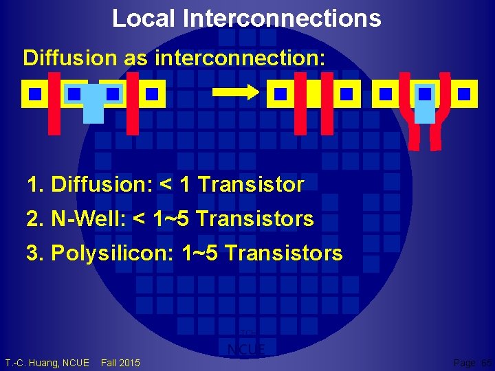
Local Interconnections Diffusion as interconnection: 1. Diffusion: < 1 Transistor 2. N-Well: < 1~5 Transistors 3. Polysilicon: 1~5 Transistors TCH T. -C. Huang, NCUE Fall 2015 NCUE Page 65

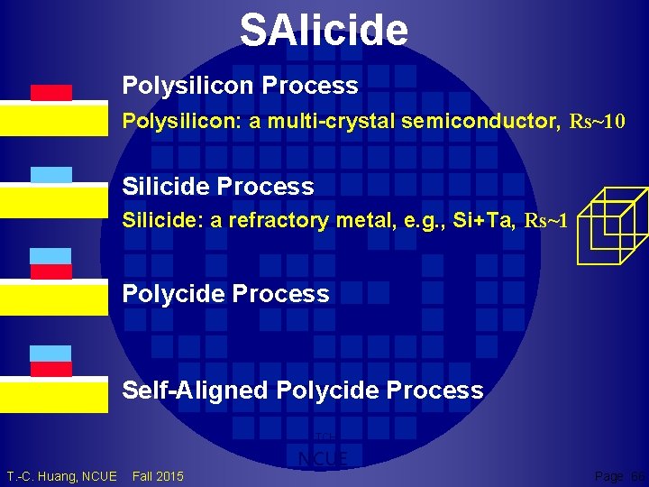
SAlicide Polysilicon Process Polysilicon: a multi-crystal semiconductor, Rs~10 Silicide Process Silicide: a refractory metal, e. g. , Si+Ta, Rs~1 Polycide Process Self-Aligned Polycide Process TCH T. -C. Huang, NCUE Fall 2015 NCUE Page 66

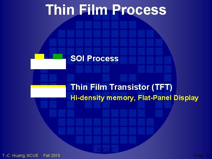
Thin Film Process SOI Process Thin Film Transistor (TFT) Hi-density memory, Flat-Panel Display TCH T. -C. Huang, NCUE Fall 2015 NCUE Page 67

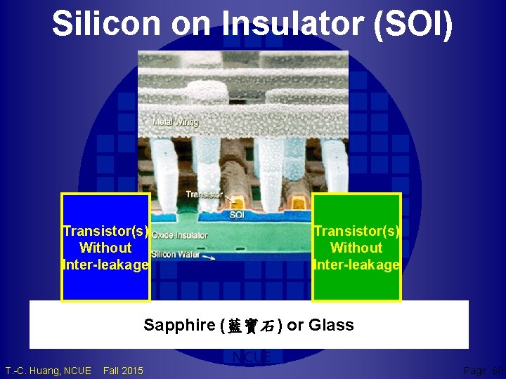
Silicon on Insulator (SOI) Transistor(s) Without Inter-leakage P bulk N bulk Sapphire (藍寶石) or Glass TCH T. -C. Huang, NCUE Fall 2015 NCUE Page 68

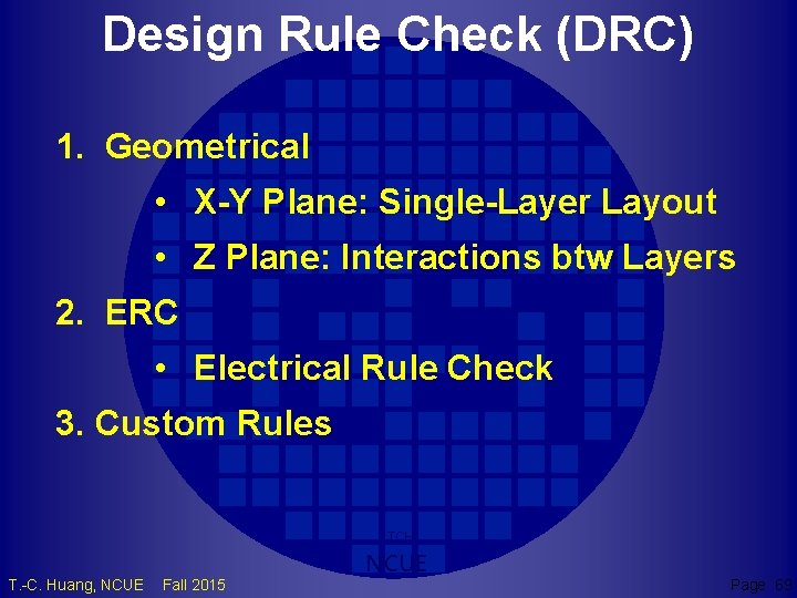
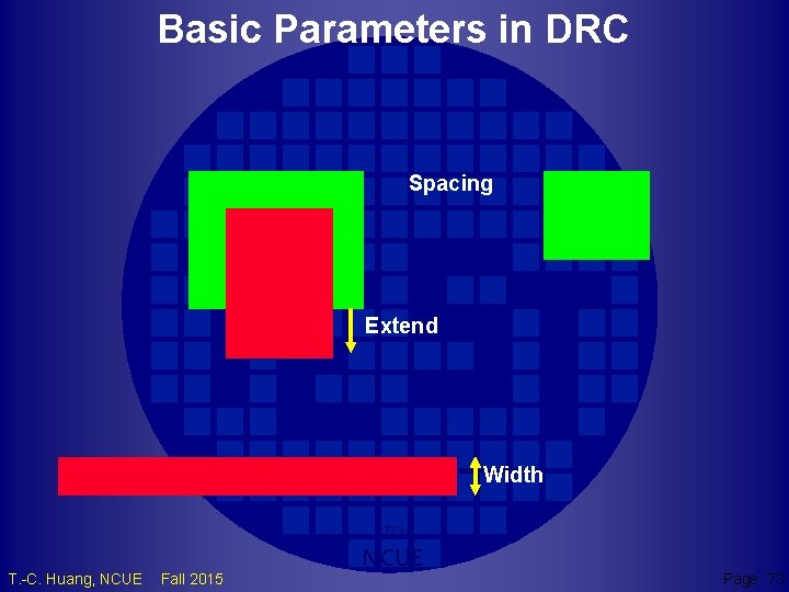
Design Rule Check (DRC) 1. Geometrical • X-Y Plane: Single-Layer Layout • Z Plane: Interactions btw Layers 2. ERC • Electrical Rule Check 3. Custom Rules TCH T. -C. Huang, NCUE Fall 2015 NCUE Page 69

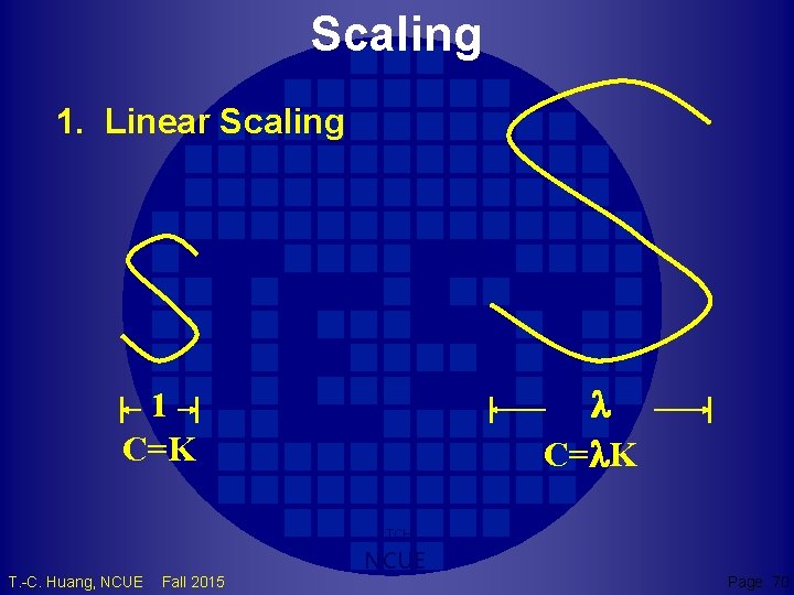
Scaling 1. Linear Scaling l C=l. K 1 C=K TCH T. -C. Huang, NCUE Fall 2015 NCUE Page 70

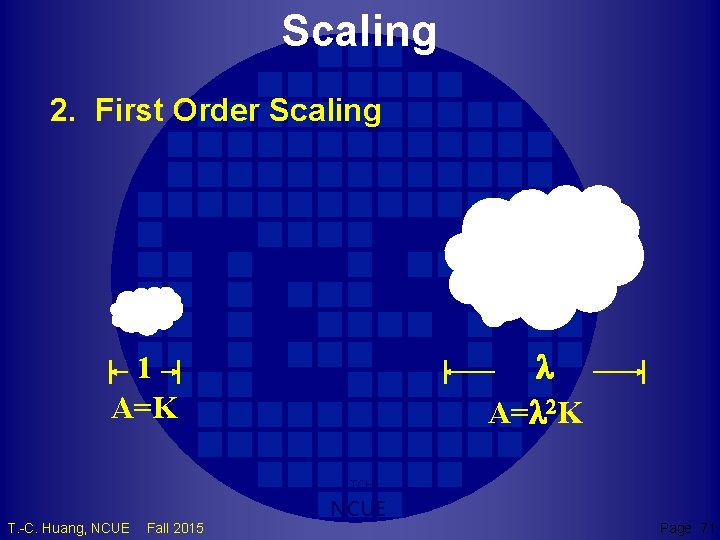
Scaling 2. First Order Scaling l A=l 2 K 1 A=K TCH T. -C. Huang, NCUE Fall 2015 NCUE Page 71

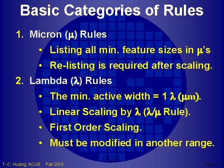
Basic Categories of Rules 1. Micron (m) Rules • Listing all min. feature sizes in m’s • Re-listing is required after scaling. 2. Lambda (l) Rules • The min. active width = 1 l (mm). • Linear Scaling by l (l/m Rule). • First Order Scaling. • Must be modified in another range. TCH T. -C. Huang, NCUE Fall 2015 NCUE Page 72

Basic Parameters in DRC Spacing Extend Width TCH T. -C. Huang, NCUE Fall 2015 NCUE Page 73

Some Rules in TSMC. 35 -2 P 4 M(P) TCH T. -C. Huang, NCUE Fall 2015 NCUE Page 74

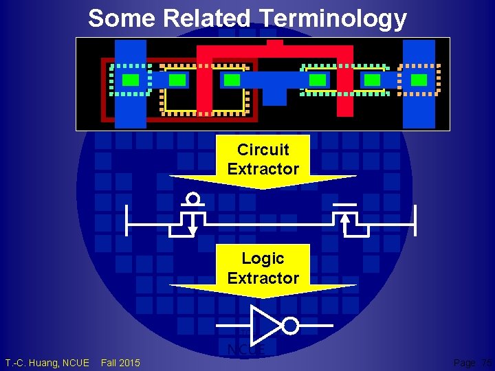
Some Related Terminology Circuit Extractor Logic Extractor TCH T. -C. Huang, NCUE Fall 2015 NCUE Page 75

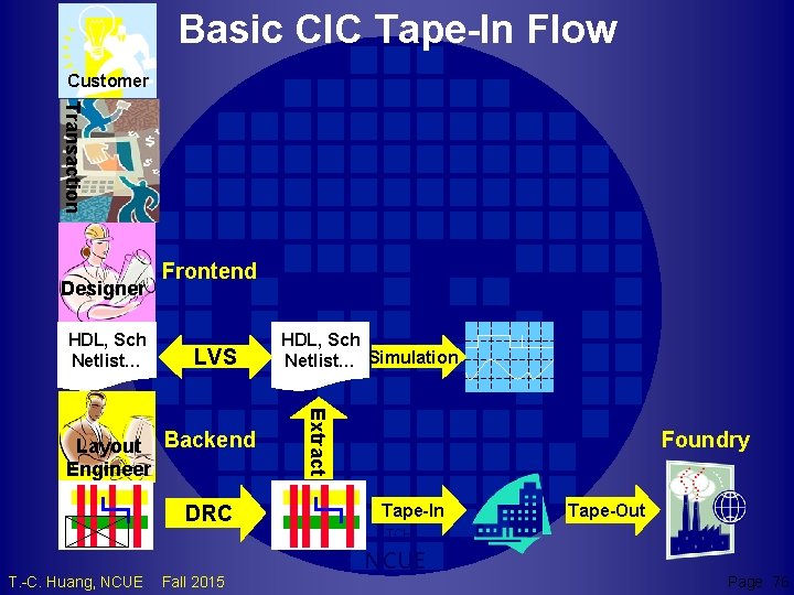
Basic CIC Tape-In Flow Customer Transaction Designer HDL, Sch Netlist… Frontend LVS DRC T. -C. Huang, NCUE Fall 2015 Extract Layout Backend Engineer HDL, Sch Netlist… Simulation Foundry Tape-In Tape-Out TCH NCUE Page 76

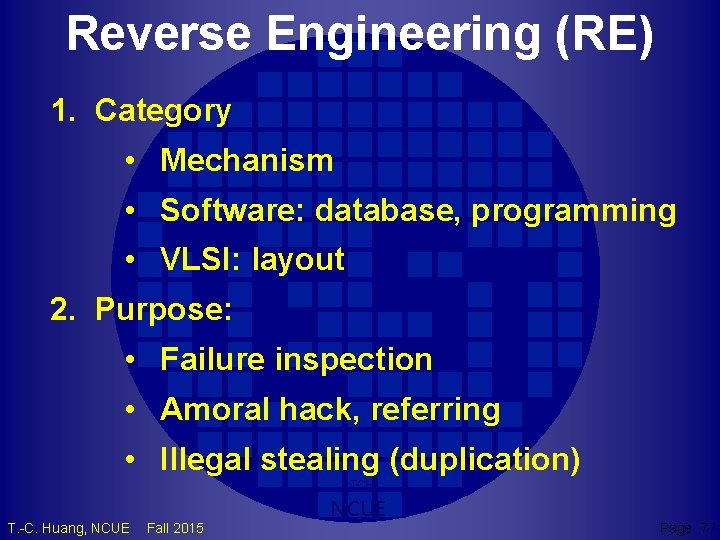
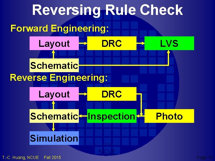
Reverse Engineering (RE) 1. Category • Mechanism • Software: database, programming • VLSI: layout 2. Purpose: • Failure inspection • Amoral hack, referring • Illegal stealing (duplication) TCH T. -C. Huang, NCUE Fall 2015 NCUE Page 77

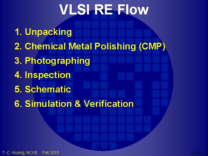
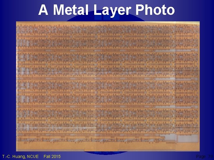
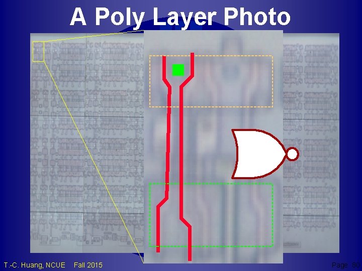
VLSI RE Flow 1. Unpacking 2. Chemical Metal Polishing (CMP) 3. Photographing 4. Inspection 5. Schematic 6. Simulation & Verification TCH T. -C. Huang, NCUE Fall 2015 NCUE Page 78

A Metal Layer Photo TCH T. -C. Huang, NCUE Fall 2015 NCUE Page 79

A Poly Layer Photo TCH T. -C. Huang, NCUE Fall 2015 NCUE Page 80

Reversing Rule Check Forward Engineering: Layout DRC LVS Schematic Reverse Engineering: Layout DRC Schematic Inspection Simulation T. -C. Huang, NCUE Fall 2015 Photo TCH NCUE Page 81