LowPower IC Design Power Estimation TsungChu Huang Dept









- Slides: 79

Low-Power IC Design Power Estimation Tsung-Chu Huang Dep’t of Electronic Eng. , Nat’l Changhua Univ. Spring 2007 Low-Power IC Design. Tsung-Chu Huang, NCUE Ch. 7 Sub-threshold Design 1 NCUE EDAT

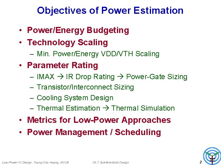
Objectives of Power Estimation • Power/Energy Budgeting • Technology Scaling – Min. Power/Energy VDD/VTH Scaling • Parameter Rating – – IMAX IR Drop Rating Power-Gate Sizing Transistor/Interconnect Sizing Cooling System Design Thermal Estimation Thermal Simulation • Metrics for Low-Power Approaches • Power Management / Scheduling Low-Power IC Design. Tsung-Chu Huang, NCUE Ch. 7 Sub-threshold Design 2 NCUE EDAT

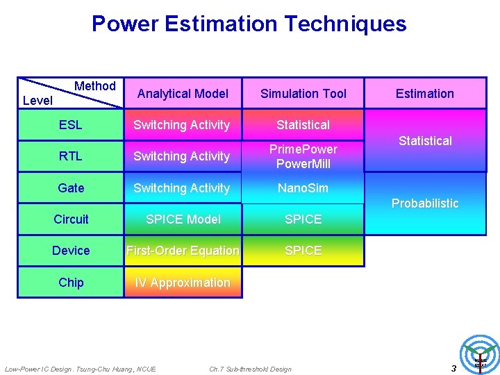
Power Estimation Techniques Method Analytical Model Simulation Tool Switching Activity Statistical RTL Switching Activity Prime. Power. Mill Gate Switching Activity Nano. Sim Level ESL Estimation Statistical Probabilistic Circuit SPICE Model SPICE Device First-Order Equation SPICE Chip IV Approximation Low-Power IC Design. Tsung-Chu Huang, NCUE Ch. 7 Sub-threshold Design 3 NCUE EDAT

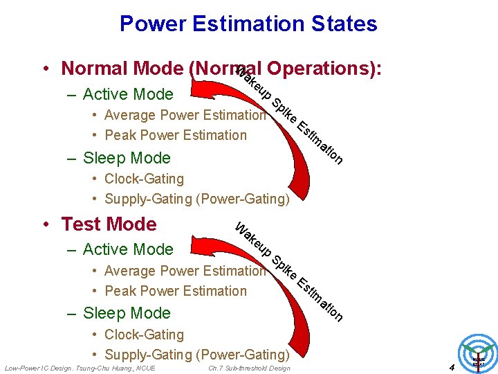
Power Estimation States W • Normal Mode (Normal ak Operations): eu p – Active Mode • Average Power Estimation • Peak Power Estimation Sp ike Es tim at – Sleep Mode io n • Clock-Gating • Supply-Gating (Power-Gating) • Test Mode – Active Mode W ak eu p Sp • Average Power Estimation ike • Peak Power Estimation – Sleep Mode Es tim at io n • Clock-Gating • Supply-Gating (Power-Gating) Low-Power IC Design. Tsung-Chu Huang, NCUE Ch. 7 Sub-threshold Design 4 NCUE EDAT

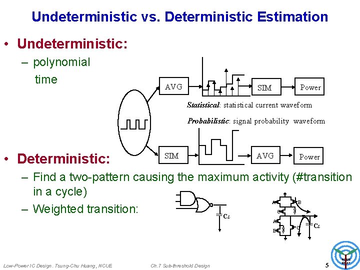
Undeterministic vs. Deterministic Estimation • Undeterministic: – polynomial time AVG Power SIM Statistical: statistical current waveform Probabilistic: signal probability waveform • Deterministic: SIM AVG Power – Find a two-pattern causing the maximum activity (#transition in a cycle) B A – Weighted transition: C F C L A B Low-Power IC Design. Tsung-Chu Huang, NCUE Ch. 7 Sub-threshold Design C CL 5 NCUE EDAT

Rough Power Estimation Wafer/Chip/Process Low-Power IC Design. Tsung-Chu Huang, NCUE Ch. 7 Sub-threshold Design 6 NCUE EDAT

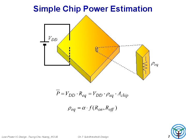
Simple Chip Power Estimation Low-Power IC Design. Tsung-Chu Huang, NCUE Ch. 7 Sub-threshold Design 7 NCUE EDAT

Simulation Low-Power IC Design. Tsung-Chu Huang, NCUE Ch. 7 Sub-threshold Design 8 NCUE EDAT

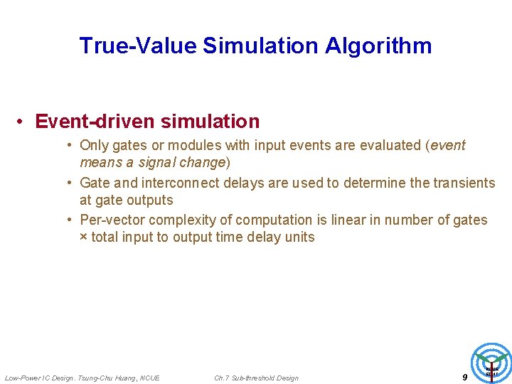
True-Value Simulation Algorithm • Event-driven simulation • Only gates or modules with input events are evaluated (event means a signal change) • Gate and interconnect delays are used to determine the transients at gate outputs • Per-vector complexity of computation is linear in number of gates × total input to output time delay units Low-Power IC Design. Tsung-Chu Huang, NCUE Ch. 7 Sub-threshold Design 9 NCUE EDAT

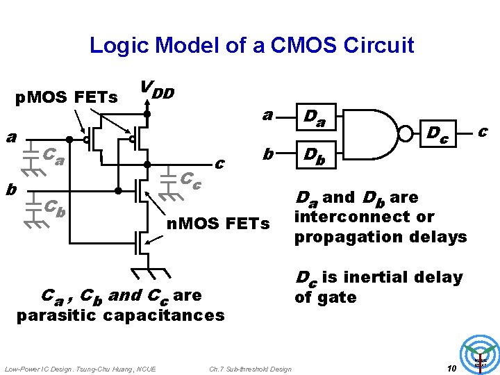
Logic Model of a CMOS Circuit p. MOS FETs a b VDD Ca Cb Cc c a Da b Db n. MOS FETs c Da and Db are interconnect or propagation delays Dc is inertial delay Ca , Cb and Cc are parasitic capacitances Low-Power IC Design. Tsung-Chu Huang, NCUE Dc Ch. 7 Sub-threshold Design of gate 10 NCUE EDAT

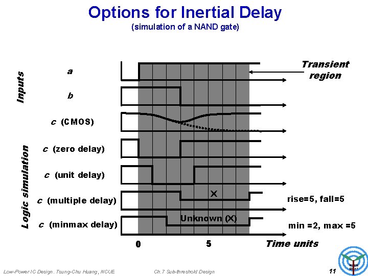
Options for Inertial Delay Inputs (simulation of a NAND gate) Transient region a b Logic simulation c (CMOS) c (zero delay) c (unit delay) X c (multiple delay) Unknown (X) c (minmax delay) 0 Low-Power IC Design. Tsung-Chu Huang, NCUE 5 Ch. 7 Sub-threshold Design rise=5, fall=5 min =2, max =5 Time units 11 NCUE EDAT

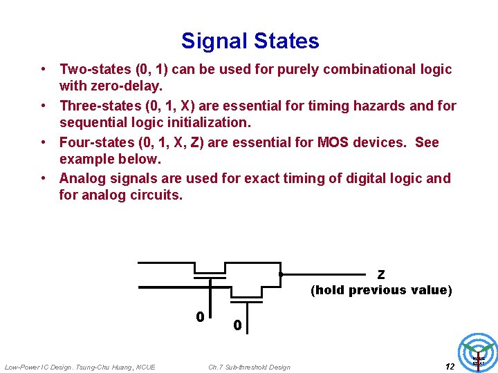
Signal States • Two-states (0, 1) can be used for purely combinational logic with zero-delay. • Three-states (0, 1, X) are essential for timing hazards and for sequential logic initialization. • Four-states (0, 1, X, Z) are essential for MOS devices. See example below. • Analog signals are used for exact timing of digital logic and for analog circuits. Z (hold previous value) 0 Low-Power IC Design. Tsung-Chu Huang, NCUE 0 Ch. 7 Sub-threshold Design 12 NCUE EDAT

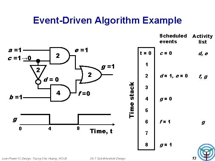
Event-Driven Algorithm Example Scheduled events 2 e =1 2 2 d=0 4 b =1 t=0 f =0 g 0 4 8 Time, t 2 Ch. 7 Sub-threshold Design d, e d = 1, e = 0 f, g 3 4 g=0 5 6 f=1 g 7 8 Low-Power IC Design. Tsung-Chu Huang, NCUE c=0 1 g =1 Time stack a =1 c =1→ 0 Activity list g=1 13 NCUE EDAT

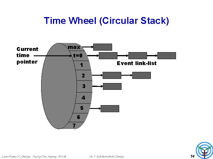
Time Wheel (Circular Stack) Current time pointer max t=0 1 Event link-list 2 3 4 5 6 7 Low-Power IC Design. Tsung-Chu Huang, NCUE Ch. 7 Sub-threshold Design 14 NCUE EDAT

Power Estimation • For every vector (changes at primary input): – At every signal node (gate output): • Count number of transitions • Compute #transitions × node capacitance × VDD 2/2 • If node capacitances are not known, use fanout approximation – often used for relative power comparison between circuits • Add pre-estimated leakage power for vector period Low-Power IC Design. Tsung-Chu Huang, NCUE Ch. 7 Sub-threshold Design 15 NCUE EDAT

Estimation of Power • Circuit is simulated by an event-driven simulator for both optimized and unoptimized gate delays. • All transitions at a gate are counted as Events[gate]. • Power consumed Events[gate] x # of fanouts. • Ref: “Effects of delay model on peak power estimation of VLSI circuits, ” Hsiao, et al. (ICCAD`97). Low-Power IC Design. Tsung-Chu Huang, NCUE Ch. 7 Sub-threshold Design 16 NCUE EDAT

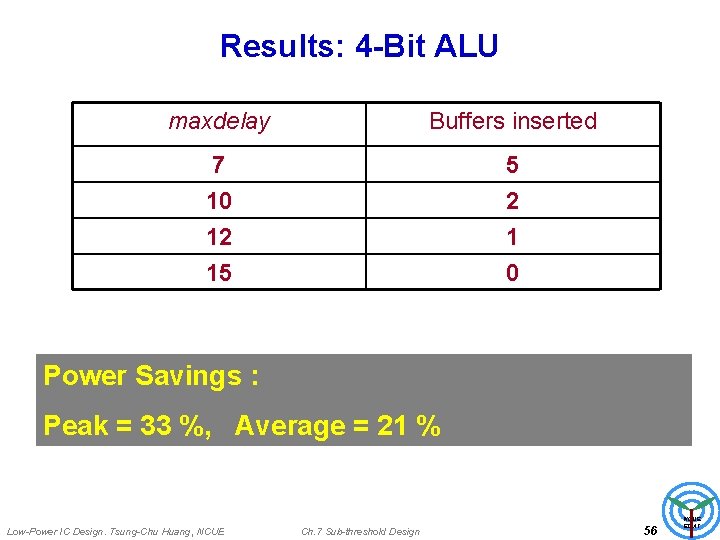
Results: 4 -Bit ALU maxdelay Buffers inserted 7 10 12 5 2 1 15 0 Power Savings : Peak = 33 %, Average = 21 % Low-Power IC Design. Tsung-Chu Huang, NCUE Ch. 7 Sub-threshold Design 17 NCUE EDAT

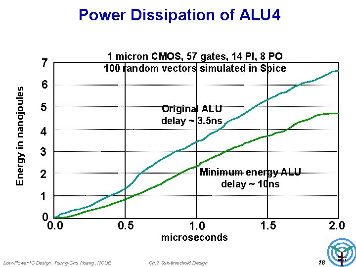
Power Dissipation of ALU 4 Energy in nanojoules 7 1 micron CMOS, 57 gates, 14 PI, 8 PO 100 random vectors simulated in Spice 6 5 Original ALU delay ~ 3. 5 ns 4 3 Minimum energy ALU delay ~ 10 ns 2 1 0 0. 5 1. 0 1. 5 2. 0 microseconds Low-Power IC Design. Tsung-Chu Huang, NCUE Ch. 7 Sub-threshold Design 18 NCUE EDAT

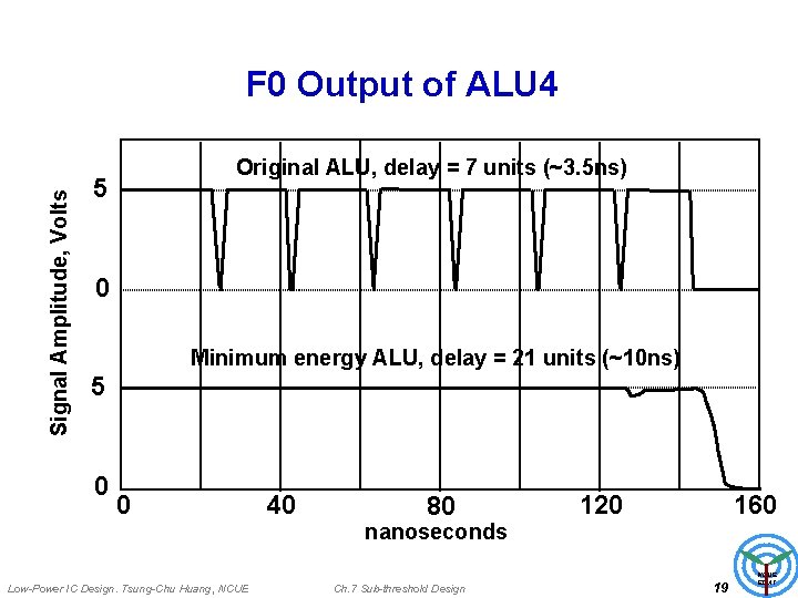
Signal Amplitude, Volts F 0 Output of ALU 4 Original ALU, delay = 7 units (~3. 5 ns) 5 0 Minimum energy ALU, delay = 21 units (~10 ns) 5 0 0 40 80 120 160 nanoseconds Low-Power IC Design. Tsung-Chu Huang, NCUE Ch. 7 Sub-threshold Design 19 NCUE EDAT

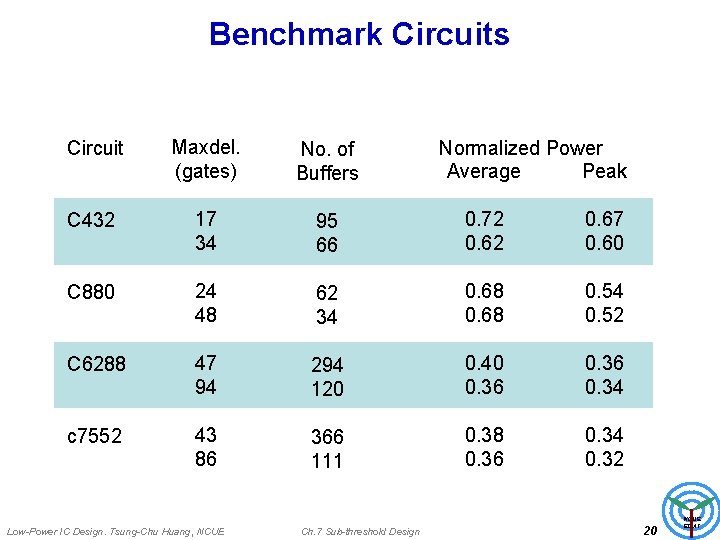
Benchmark Circuits Circuit Maxdel. (gates) No. of Buffers C 432 17 34 95 66 0. 72 0. 67 0. 60 C 880 24 48 62 34 0. 68 0. 54 0. 52 C 6288 47 94 294 120 0. 40 0. 36 0. 34 c 7552 43 86 366 111 0. 38 0. 36 0. 34 0. 32 Low-Power IC Design. Tsung-Chu Huang, NCUE Ch. 7 Sub-threshold Design Normalized Power Average Peak 20 NCUE EDAT

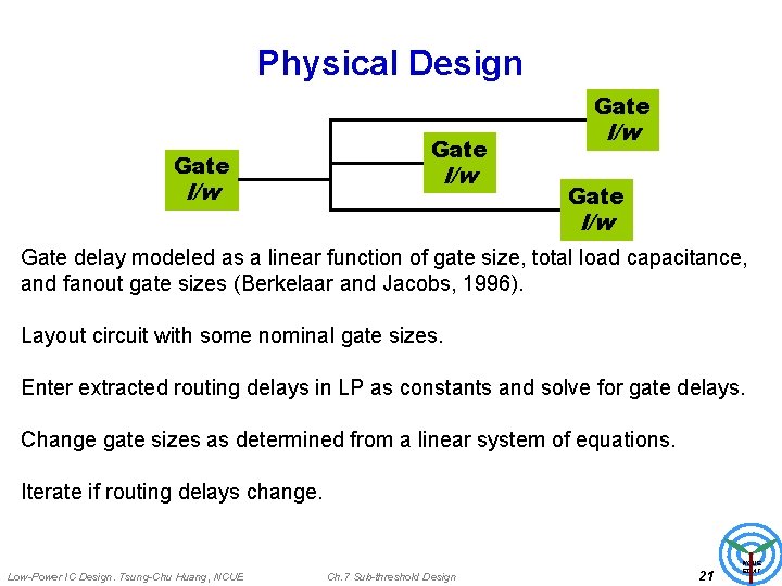
Physical Design Gate l/w Gate delay modeled as a linear function of gate size, total load capacitance, and fanout gate sizes (Berkelaar and Jacobs, 1996). Layout circuit with some nominal gate sizes. Enter extracted routing delays in LP as constants and solve for gate delays. Change gate sizes as determined from a linear system of equations. Iterate if routing delays change. Low-Power IC Design. Tsung-Chu Huang, NCUE Ch. 7 Sub-threshold Design 21 NCUE EDAT

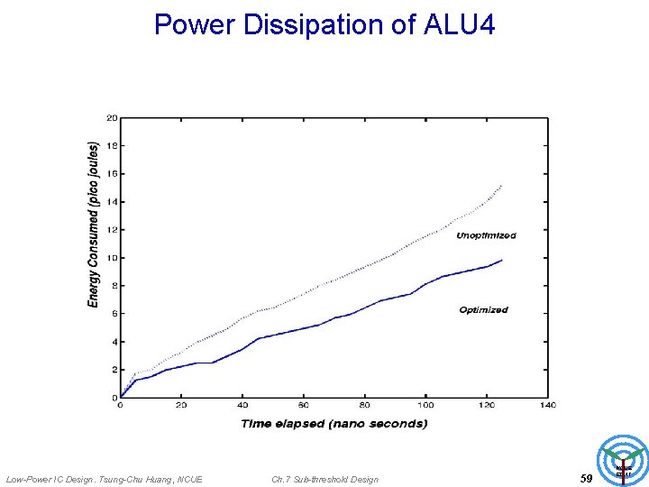
Power Dissipation of ALU 4 Low-Power IC Design. Tsung-Chu Huang, NCUE Ch. 7 Sub-threshold Design 22 NCUE EDAT

References • • • R. Fourer, D. M. Gay and B. W. Kernighan, AMPL: A Modeling Language for Mathematical Programming, South San Francisco: The Scientific Press, 1993. M. Berkelaar and E. Jacobs, “Using Gate Sizing to Reduce Glitch Power, ” Proc. Pro. RISC Workshop, Mierlo, The Netherlands, Nov. 1996, pp. 183 -188. V. D. Agrawal, “Low Power Design by Hazard Filtering, ” Proc. 10 th Int’l Conf. VLSI Design, Jan. 1997, pp. 193 -197. V. D. Agrawal, M. L. Bushnell, G. Parthasarathy and R. Ramadoss, “Digital Circuit Design for Minimum Transient Energy and Linear Programming Method, ” Proc. 12 th Int’l Conf. VLSI Design, Jan. 1999, pp. 434 -439. M. Hsiao, E. M. Rudnick and J. H. Patel, “Effects of Delay Model in Peak Power Estimation of VLSI Circuits, ” Proc. ICCAD, Nov. 1997, pp. 45 -51. T. Raja, A Reduced Constraint Set Linear Program for Low Power Design of Digital Circuits, Master’s Thesis, Rutgers Univ. , New Jersey, 2002. Low-Power IC Design. Tsung-Chu Huang, NCUE Ch. 7 Sub-threshold Design 23 NCUE EDAT

Conclusion • Glitch-free design through LP: constraint-set is linear in the size of the circuit. • LP solution: – Eliminates glitches at all gate outputs, – Holds I/O delay within specification, and – Combines path-balancing and hazard-filtering to minimize the number of delay buffers. • Linear constraint set LP produces results exactly identical to the LP requiring exponential constraint-set. • Results show peak power savings up to 68% and average power savings up to 64%. Low-Power IC Design. Tsung-Chu Huang, NCUE Ch. 7 Sub-threshold Design 24 NCUE EDAT

SPICE Simulation Low-Power IC Design. Tsung-Chu Huang, NCUE Ch. 7 Sub-threshold Design 25 NCUE EDAT

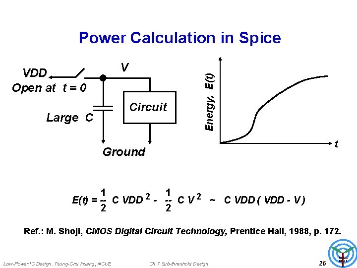
V VDD Open at t = 0 Circuit Large C Energy, E(t) Power Calculation in Spice t Ground 1 1 2 E(t) = -- C VDD - -- C V 2 ~ C VDD ( VDD - V ) 2 2 Ref. : M. Shoji, CMOS Digital Circuit Technology, Prentice Hall, 1988, p. 172. Low-Power IC Design. Tsung-Chu Huang, NCUE Ch. 7 Sub-threshold Design 26 NCUE EDAT

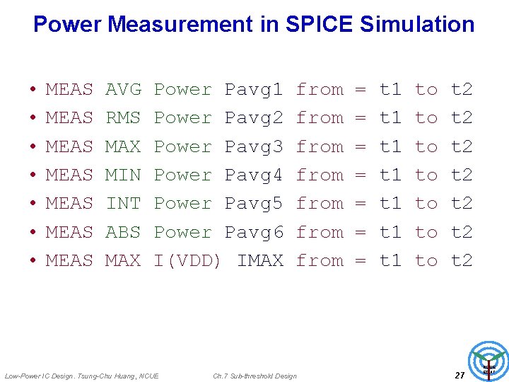
Power Measurement in SPICE Simulation • • MEAS MEAS AVG RMS MAX MIN INT ABS MAX Power Pavg 1 Power Pavg 2 Power Pavg 3 Power Pavg 4 Power Pavg 5 Power Pavg 6 I(VDD) IMAX Low-Power IC Design. Tsung-Chu Huang, NCUE from from Ch. 7 Sub-threshold Design = = = = t 1 t 1 to to t 2 t 2 27 NCUE EDAT

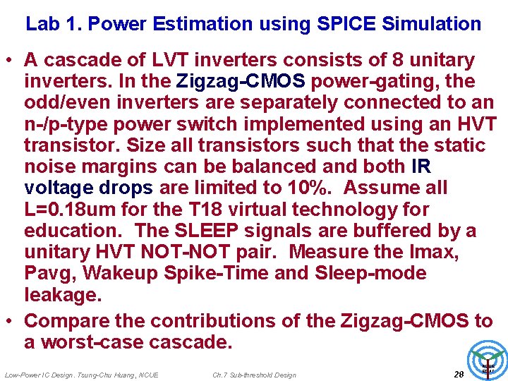
Lab 1. Power Estimation using SPICE Simulation • A cascade of LVT inverters consists of 8 unitary inverters. In the Zigzag-CMOS power-gating, the odd/even inverters are separately connected to an n-/p-type power switch implemented using an HVT transistor. Size all transistors such that the static noise margins can be balanced and both IR voltage drops are limited to 10%. Assume all L=0. 18 um for the T 18 virtual technology for education. The SLEEP signals are buffered by a unitary HVT NOT-NOT pair. Measure the Imax, Pavg, Wakeup Spike-Time and Sleep-mode leakage. • Compare the contributions of the Zigzag-CMOS to a worst-case cascade. Low-Power IC Design. Tsung-Chu Huang, NCUE Ch. 7 Sub-threshold Design 28 NCUE EDAT

Switch-Level Simulation Low-Power IC Design. Tsung-Chu Huang, NCUE Ch. 7 Sub-threshold Design 29 NCUE EDAT

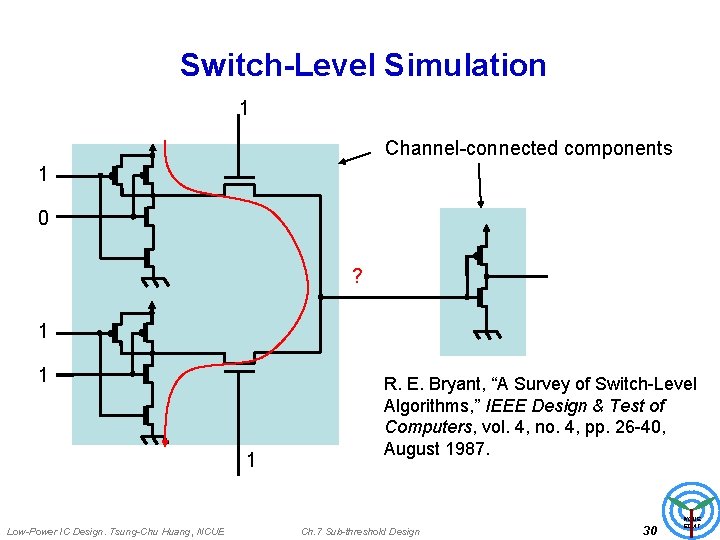
Switch-Level Simulation 1 Channel-connected components 1 0 ? 1 1 1 Low-Power IC Design. Tsung-Chu Huang, NCUE R. E. Bryant, “A Survey of Switch-Level Algorithms, ” IEEE Design & Test of Computers, vol. 4, no. 4, pp. 26 -40, August 1987. Ch. 7 Sub-threshold Design 30 NCUE EDAT

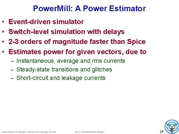
Power. Mill: A Power Estimator • • Event-driven simulator Switch-level simulation with delays 2 -3 orders of magnitude faster than Spice Estimates power for given vectors, due to – Instantaneous, average and rms currents – Steady-state transitions and glitches – Short-circuit and leakage currents Low-Power IC Design. Tsung-Chu Huang, NCUE Ch. 7 Sub-threshold Design 31 NCUE EDAT

Power. Mill (Cont. ) • Determines current density and voltage drop in the power net • Points to potential problem areas on a VLSI chip for EM failures, ground bounce, excessive voltage drop, heating • Reference: C. Deng, “Power Analysis for CMOS/Bi. CMOS Circuits, ” Proc. International Workshop on Low Power Design, April 1994, pp. 38. Low-Power IC Design. Tsung-Chu Huang, NCUE Ch. 7 Sub-threshold Design 32 NCUE EDAT

Entice-Aspen: Gate-level Tool • Gate-level circuit is partitioned into cells. • Cells are simulated in Spice for power dissipation for all possible input events. • Logic simulation determines the events at cell inputs, adding the corresponding power dissipated by each cell. • B. J. George, D. Gossain, S. C. Tyler, M. G. Wloka, and G. K. H. Yeap, “Power Analysis and Characterization for Semi. Custom Design, ” Proc. International Workshop on Low Power Design, April 1994, pp. 215 -218. Low-Power IC Design. Tsung-Chu Huang, NCUE Ch. 7 Sub-threshold Design 33 NCUE EDAT

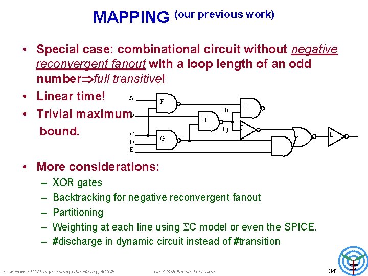
MAPPING (our previous work) • Special case: combinational circuit without negative reconvergent fanout with a loop length of an odd number full transitive! A • Linear time! F I Hi B • Trivial maximum H J Hj bound. C L G K D E • More considerations: – – – XOR gates Backtracking for negative reconvergent fanout Partitioning Weighting at each line using C model or even the SPICE. #discharge in dynamic circuit instead of #transition Low-Power IC Design. Tsung-Chu Huang, NCUE Ch. 7 Sub-threshold Design 34 NCUE EDAT

Gate-Level Simulation -- Probabilistic Power Estimation Low-Power IC Design. Tsung-Chu Huang, NCUE Ch. 7 Sub-threshold Design 35 NCUE EDAT

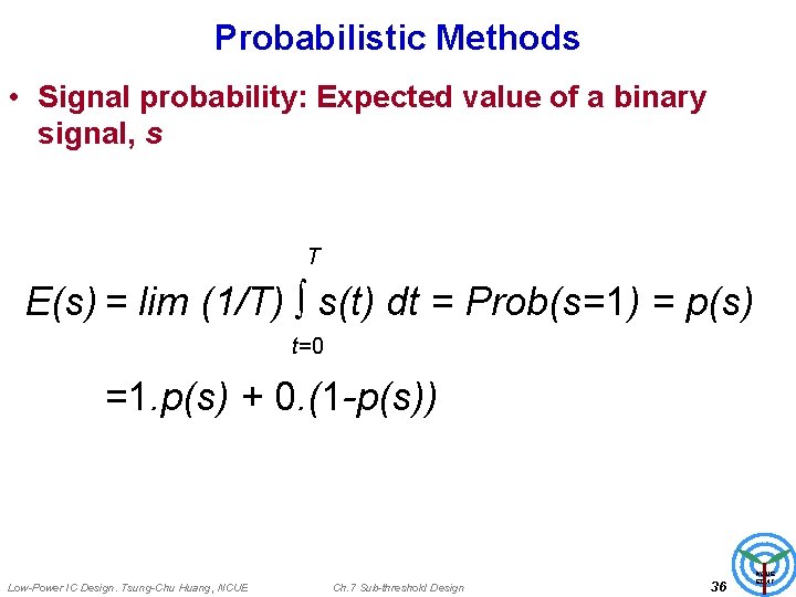
Probabilistic Methods • Signal probability: Expected value of a binary signal, s T E(s) = lim (1/T) ∫ s(t) dt = Prob(s=1) = p(s) t=0 =1. p(s) + 0. (1 -p(s)) Low-Power IC Design. Tsung-Chu Huang, NCUE Ch. 7 Sub-threshold Design 36 NCUE EDAT

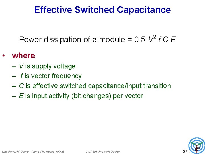
Effective Switched Capacitance Power dissipation of a module = 0. 5 V 2 f C E • where – – V is supply voltage f is vector frequency C is effective switched capacitance/input transition E is input activity (bit changes) per vector Low-Power IC Design. Tsung-Chu Huang, NCUE Ch. 7 Sub-threshold Design 37 NCUE EDAT

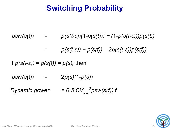
Switching Probability psw(s(t)) = p(s(t-ε))(1 -p(s(t))) + (1 -p(s(t-ε)))p(s(t)) = p(s(t-ε)) + p(s(t)) – 2 p(s(t-ε))p(s(t)) If p(s(t-ε)) = p(s(t)) = p(s), then psw(s(t)) = Dynamic power Low-Power IC Design. Tsung-Chu Huang, NCUE 2 p(s)(1 -p(s)) = 0. 5 CVDD 2 psw(s(t)) f Ch. 7 Sub-threshold Design 38 NCUE EDAT

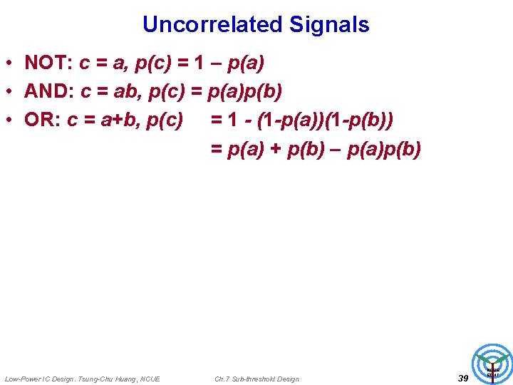
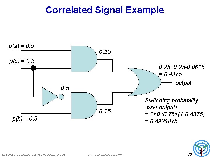
Uncorrelated Signals • NOT: c = a, p(c) = 1 – p(a) • AND: c = ab, p(c) = p(a)p(b) • OR: c = a+b, p(c) = 1 - (1 -p(a))(1 -p(b)) = p(a) + p(b) – p(a)p(b) Low-Power IC Design. Tsung-Chu Huang, NCUE Ch. 7 Sub-threshold Design 39 NCUE EDAT

Correlated Signal Example p(a) = 0. 5 0. 25 p(c) = 0. 5 0. 25+0. 25 -0. 0625 = 0. 4375 output 0. 5 0. 25 p(b) = 0. 5 Low-Power IC Design. Tsung-Chu Huang, NCUE Ch. 7 Sub-threshold Design Switching probability psw(output) = 2× 0. 4375×(1 -0. 4375) = 0. 4921875 40 NCUE EDAT

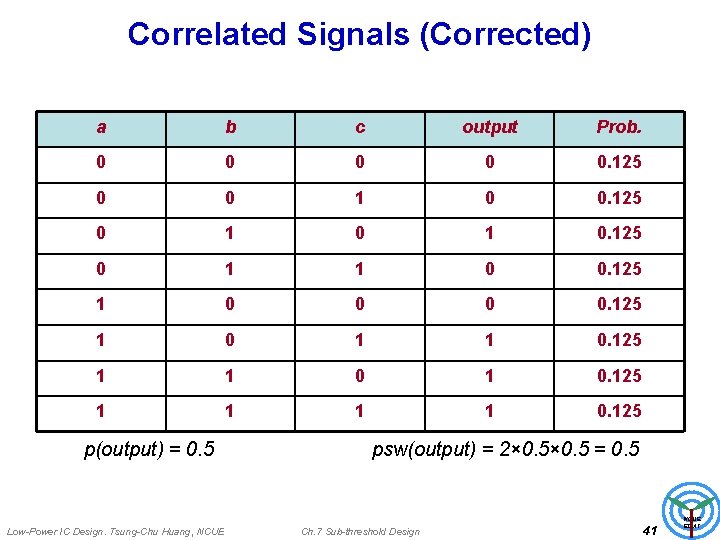
Correlated Signals (Corrected) a b c output Prob. 0 0 0. 125 0 0 1 0 0. 125 0 1 1 0 0. 125 1 0 1 1 0. 125 p(output) = 0. 5 Low-Power IC Design. Tsung-Chu Huang, NCUE psw(output) = 2× 0. 5 = 0. 5 Ch. 7 Sub-threshold Design 41 NCUE EDAT

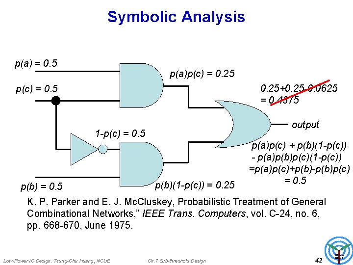
Symbolic Analysis p(a) = 0. 5 p(a)p(c) = 0. 25+0. 25 -0. 0625 = 0. 4375 p(c) = 0. 5 output 1 -p(c) = 0. 5 p(b)(1 -p(c)) = 0. 25 p(a)p(c) + p(b)(1 -p(c)) - p(a)p(b)p(c)(1 -p(c)) =p(a)p(c)+p(b)-p(b)p(c) = 0. 5 K. P. Parker and E. J. Mc. Cluskey, Probabilistic Treatment of General Combinational Networks, ” IEEE Trans. Computers, vol. C-24, no. 6, pp. 668 -670, June 1975. Low-Power IC Design. Tsung-Chu Huang, NCUE Ch. 7 Sub-threshold Design 42 NCUE EDAT

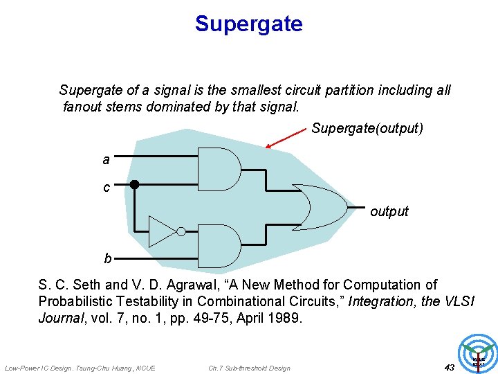
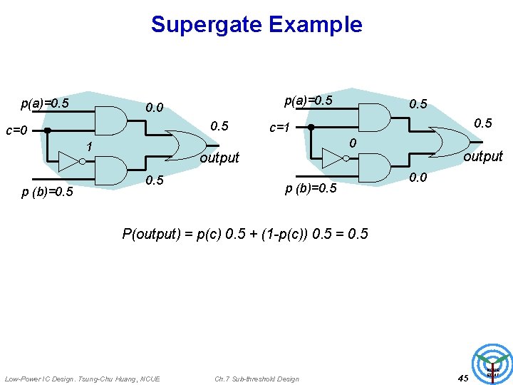
Supergate of a signal is the smallest circuit partition including all fanout stems dominated by that signal. Supergate(output) a c output b S. C. Seth and V. D. Agrawal, “A New Method for Computation of Probabilistic Testability in Combinational Circuits, ” Integration, the VLSI Journal, vol. 7, no. 1, pp. 49 -75, April 1989. Low-Power IC Design. Tsung-Chu Huang, NCUE Ch. 7 Sub-threshold Design 43 NCUE EDAT

PREDICT Algorithm • To calculate p(output), enumerate signal states at fanout signal(s) – c in this example. • For each case i, compute pi(output) separately. • Compute p(output) = p(c)p 1(output) + (1 -p(c))p 0(output) Low-Power IC Design. Tsung-Chu Huang, NCUE Ch. 7 Sub-threshold Design 44 NCUE EDAT

Supergate Example p(a)=0. 5 c=0 1 p (b)=0. 5 p(a)=0. 5 0. 0 0. 5 c=1 0 output 0. 5 p (b)=0. 5 output 0. 0 P(output) = p(c) 0. 5 + (1 -p(c)) 0. 5 = 0. 5 Low-Power IC Design. Tsung-Chu Huang, NCUE Ch. 7 Sub-threshold Design 45 NCUE EDAT

Other Signal Probability Methods • Weighted averaging – B. Krishnamurthy and I. G. Tollis, “Improved Techniques for Estimating Signal Probabilities, ” IEEE Trans. Computers, vol. C-38, no. 7, pp. 1245 -1251, July 1989. • Cutting algorithm – J. Savir, G. Ditlow and P. Bardell, “Random Pattern Testability, ” IEEE Trans. Computers, vol. C-33, no. 1, pp. 79 -90, Jan. 1989. • OBDD – R. E. Bryant, “Graph-Based Algorithms for Boolean Function Manipulation, ” IEEE Trans. Computers, vol. C-35, no. 8, pp. 677 -691, Aug. 1989. • Transition density – F. N. Najm, “Transition Density: A New Measure of Activity in Digital Circuits, ” IEEE Trans. CAD, vol. 12, no. 2, pp. 310 -323, Feb. 1993. Low-Power IC Design. Tsung-Chu Huang, NCUE Ch. 7 Sub-threshold Design 46 NCUE EDAT

Working with Delays • Signal probability methods do not take delays into account. Hence, glitch power is not included. • Timed symbolic simulation – A Ghosh, S. Devadas, K. Keutzer and J. White, “Estimation of Average Switching Activity in Combinational and Sequential Circuits, ” Proc. 29 th Design Automation Conf. , June 1992, pp. 253 -259. • Probability waveform simulation – C. -S. Ding, C. -Y. Tsui and M. Pedram, “Gate-Level Power Estimation Using Tagged Probabilistic Simulation, ” IEEE Trans. CAD, vol. 17, no. 11, pp. 1099 -1107, Nov. 1998. Low-Power IC Design. Tsung-Chu Huang, NCUE Ch. 7 Sub-threshold Design 47 NCUE EDAT

RTL Simulation -- Statistical Power Estimation Low-Power IC Design. Tsung-Chu Huang, NCUE Ch. 7 Sub-threshold Design 48 NCUE EDAT

RTL Power Estimation • Two step procedure: – Behavioral simulation to collect the input statistics for all modules in RTL description – Develop power macro-model for each module and sum the power • Q. Wu, C. -S. Ding, C. -T. Hsieh, and M. Pedram, “Statistical Design of Macro-Models for RT-Level Power Estimation, ” Proc. Second Asia-Pacific Design Automation Conference, Jan. 1997. Low-Power IC Design. Tsung-Chu Huang, NCUE Ch. 7 Sub-threshold Design 49 NCUE EDAT

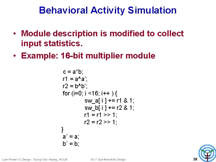
Behavioral Activity Simulation • Module description is modified to collect input statistics. • Example: 16 -bit multiplier module c = a*b; r 1 = a^a’; r 2 = b^b’; for (i=0; i <16; i++ ) { sw_a[ i ] += r 1 & 1; sw_b[ i ] += r 2 & 1; r 1 = r 1 >> 1; r 2 = r 2 >> 1; } a’ = a; b’ = b; Low-Power IC Design. Tsung-Chu Huang, NCUE Ch. 7 Sub-threshold Design 50 NCUE EDAT

Power Macro-Model • Develop analytic models for estimating the switched capacitance as a function of circuit complexity and technology/library parameters. OR • Synthesize the circuit and then estimate power dissipation by simulation with random vectors. • Both methods determine effective switched capacitance per input transition. Low-Power IC Design. Tsung-Chu Huang, NCUE Ch. 7 Sub-threshold Design 51 NCUE EDAT

Estimation of Power • Circuit is simulated by an event-driven simulator for both optimized and unoptimized gate delays. • All transitions at a gate are counted as Events[gate]. • Power consumed Events[gate] x # of fanouts. • Ref: “Effects of delay model on peak power estimation of VLSI circuits, ” Hsiao, et al. (ICCAD`97). Low-Power IC Design. Tsung-Chu Huang, NCUE Ch. 7 Sub-threshold Design 52 NCUE EDAT

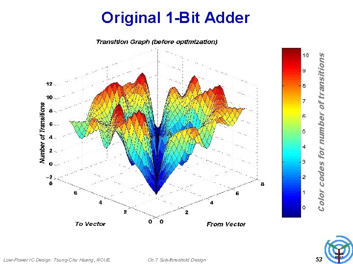
Color codes for number of transitions Original 1 -Bit Adder Low-Power IC Design. Tsung-Chu Huang, NCUE Ch. 7 Sub-threshold Design 53 NCUE EDAT

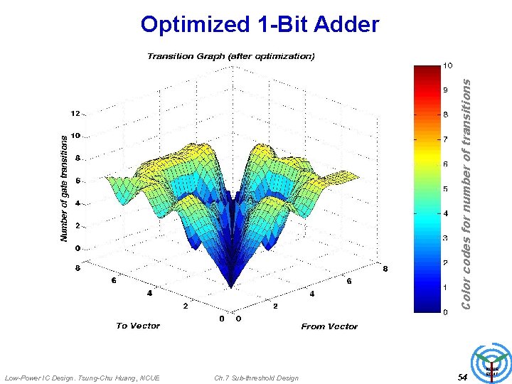
Color codes for number of transitions Optimized 1 -Bit Adder Low-Power IC Design. Tsung-Chu Huang, NCUE Ch. 7 Sub-threshold Design 54 NCUE EDAT

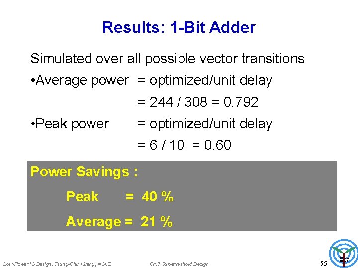
Results: 1 -Bit Adder Simulated over all possible vector transitions • Average power = optimized/unit delay = 244 / 308 = 0. 792 • Peak power = optimized/unit delay = 6 / 10 = 0. 60 Power Savings : Peak = 40 % Average = 21 % Low-Power IC Design. Tsung-Chu Huang, NCUE Ch. 7 Sub-threshold Design 55 NCUE EDAT

Results: 4 -Bit ALU maxdelay Buffers inserted 7 10 12 5 2 1 15 0 Power Savings : Peak = 33 %, Average = 21 % Low-Power IC Design. Tsung-Chu Huang, NCUE Ch. 7 Sub-threshold Design 56 NCUE EDAT

Benchmark Circuits Circuit Maxdel. (gates) No. of Buffers C 432 17 34 95 66 0. 72 0. 67 0. 60 C 880 24 48 62 34 0. 68 0. 54 0. 52 C 6288 47 94 294 120 0. 40 0. 36 0. 34 c 7552 43 86 366 111 0. 38 0. 36 0. 34 0. 32 Low-Power IC Design. Tsung-Chu Huang, NCUE Ch. 7 Sub-threshold Design Normalized Power Average Peak 57 NCUE EDAT

Physical Design Gate l/w Gate delay modeled as a linear function of gate size, total load capacitance, and fanout gate sizes (Berkelaar and Jacobs, 1996). Layout circuit with some nominal gate sizes. Enter extracted routing delays in LP as constants and solve for gate delays. Change gate sizes as determined from a linear system of equations. Iterate if routing delays change. Low-Power IC Design. Tsung-Chu Huang, NCUE Ch. 7 Sub-threshold Design 58 NCUE EDAT

Power Dissipation of ALU 4 Low-Power IC Design. Tsung-Chu Huang, NCUE Ch. 7 Sub-threshold Design 59 NCUE EDAT

References • • • R. Fourer, D. M. Gay and B. W. Kernighan, AMPL: A Modeling Language for Mathematical Programming, South San Francisco: The Scientific Press, 1993. M. Berkelaar and E. Jacobs, “Using Gate Sizing to Reduce Glitch Power, ” Proc. Pro. RISC Workshop, Mierlo, The Netherlands, Nov. 1996, pp. 183 -188. V. D. Agrawal, “Low Power Design by Hazard Filtering, ” Proc. 10 th Int’l Conf. VLSI Design, Jan. 1997, pp. 193 -197. V. D. Agrawal, M. L. Bushnell, G. Parthasarathy and R. Ramadoss, “Digital Circuit Design for Minimum Transient Energy and Linear Programming Method, ” Proc. 12 th Int’l Conf. VLSI Design, Jan. 1999, pp. 434 -439. M. Hsiao, E. M. Rudnick and J. H. Patel, “Effects of Delay Model in Peak Power Estimation of VLSI Circuits, ” Proc. ICCAD, Nov. 1997, pp. 45 -51. T. Raja, A Reduced Constraint Set Linear Program for Low Power Design of Digital Circuits, Master’s Thesis, Rutgers Univ. , New Jersey, 2002. Low-Power IC Design. Tsung-Chu Huang, NCUE Ch. 7 Sub-threshold Design 60 NCUE EDAT

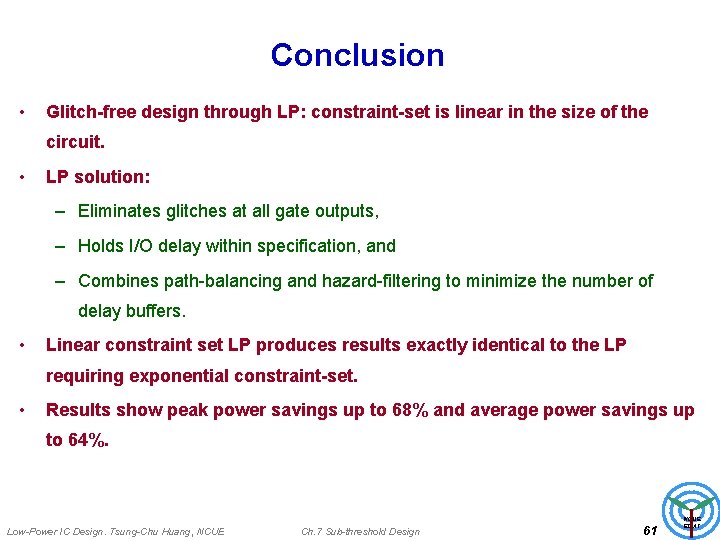
Conclusion • Glitch-free design through LP: constraint-set is linear in the size of the circuit. • LP solution: – Eliminates glitches at all gate outputs, – Holds I/O delay within specification, and – Combines path-balancing and hazard-filtering to minimize the number of delay buffers. • Linear constraint set LP produces results exactly identical to the LP requiring exponential constraint-set. • Results show peak power savings up to 68% and average power savings up to 64%. Low-Power IC Design. Tsung-Chu Huang, NCUE Ch. 7 Sub-threshold Design 61 NCUE EDAT

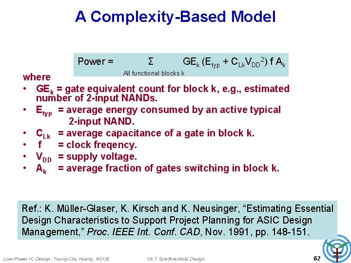
A Complexity-Based Model Power = Σ GEk (Etyp + CLk. VDD 2) f Ak All functional blocks k where • GEk = gate equivalent count for block k, e. g. , estimated number of 2 -input NANDs. • Etyp = average energy consumed by an active typical 2 -input NAND. • CLk = average capacitance of a gate in block k. • f = clock freqency. • VDD = supply voltage. • Ak = average fraction of gates switching in block k. Ref. : K. Müller-Glaser, K. Kirsch and K. Neusinger, “Estimating Essential Design Characteristics to Support Project Planning for ASIC Design Management, ” Proc. IEEE Int. Conf. CAD, Nov. 1991, pp. 148 -151. Low-Power IC Design. Tsung-Chu Huang, NCUE Ch. 7 Sub-threshold Design 62 NCUE EDAT

Improving Complexity Models • Treat logic, memory, interconnects and clock tree, separately • For example, a memory array may not be modeled as equivalent NAND gates, but as a memory cell. Low-Power IC Design. Tsung-Chu Huang, NCUE Ch. 7 Sub-threshold Design 63 NCUE EDAT

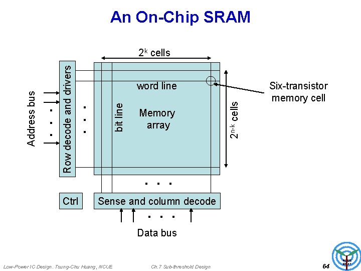
An On-Chip SRAM Row decode and drivers Ctrl Memory array 2 n-k cells bit line word line . . . Address bus 2 k cells Six-transistor memory cell . . . Sense and column decode . . . Data bus Low-Power IC Design. Tsung-Chu Huang, NCUE Ch. 7 Sub-threshold Design 64 NCUE EDAT

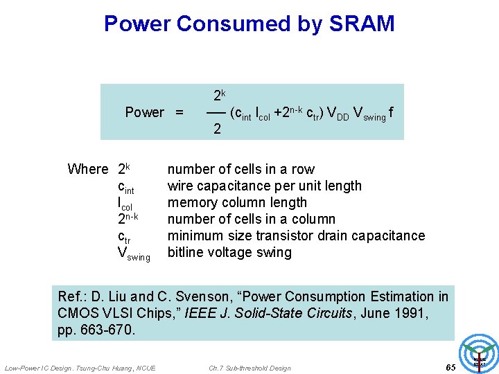
Power Consumed by SRAM Power = Where 2 k cint lcol 2 n-k ctr Vswing 2 k ── (cint lcol +2 n-k ctr) VDD Vswing f 2 number of cells in a row wire capacitance per unit length memory column length number of cells in a column minimum size transistor drain capacitance bitline voltage swing Ref. : D. Liu and C. Svenson, “Power Consumption Estimation in CMOS VLSI Chips, ” IEEE J. Solid-State Circuits, June 1991, pp. 663 -670. Low-Power IC Design. Tsung-Chu Huang, NCUE Ch. 7 Sub-threshold Design 65 NCUE EDAT

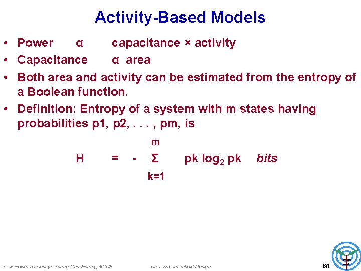
Activity-Based Models • Power α capacitance × activity • Capacitance α area • Both area and activity can be estimated from the entropy of a Boolean function. • Definition: Entropy of a system with m states having probabilities p 1, p 2, . . . , pm, is m H = - Σ pk log 2 pk bits k=1 Low-Power IC Design. Tsung-Chu Huang, NCUE Ch. 7 Sub-threshold Design 66 NCUE EDAT

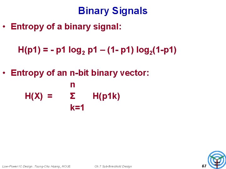
Binary Signals • Entropy of a binary signal: H(p 1) = - p 1 log 2 p 1 – (1 - p 1) log 2(1 -p 1) • Entropy of an n-bit binary vector: n H(X) = Σ H(p 1 k) k=1 Low-Power IC Design. Tsung-Chu Huang, NCUE Ch. 7 Sub-threshold Design 67 NCUE EDAT

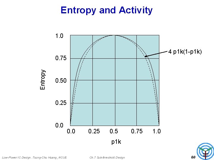
Entropy and Activity 1. 0 4 p 1 k(1 -p 1 k) Entropy 0. 75 0. 50 0. 25 0. 75 1. 0 p 1 k Low-Power IC Design. Tsung-Chu Huang, NCUE Ch. 7 Sub-threshold Design 68 NCUE EDAT

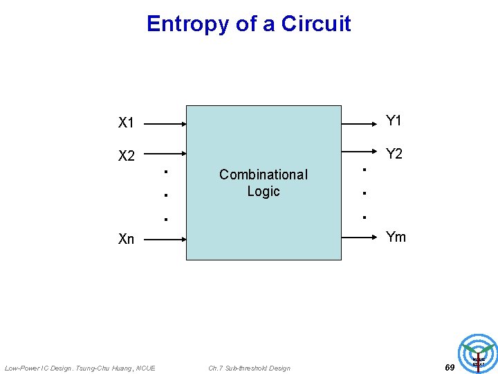
Entropy of a Circuit Y 1 X 2 . . . Combinational Logic Ym Xn Low-Power IC Design. Tsung-Chu Huang, NCUE . . . Y 2 Ch. 7 Sub-threshold Design 69 NCUE EDAT

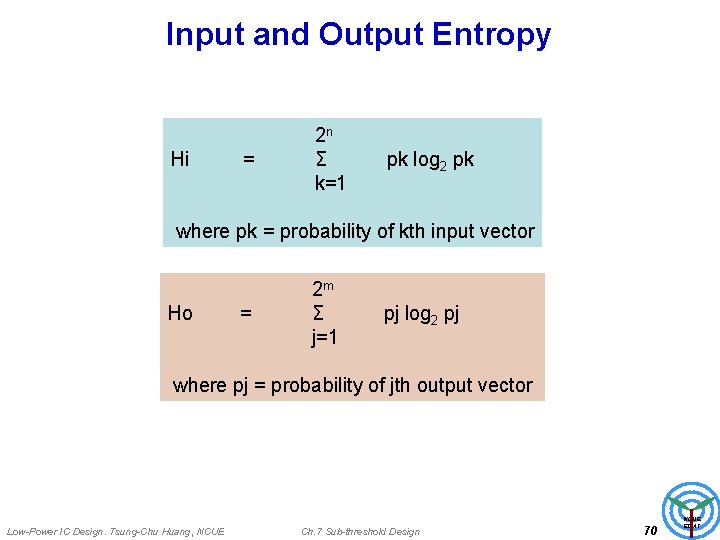
Input and Output Entropy Hi = 2 n Σ k=1 pk log 2 pk where pk = probability of kth input vector Ho = 2 m Σ j=1 pj log 2 pj where pj = probability of jth output vector Low-Power IC Design. Tsung-Chu Huang, NCUE Ch. 7 Sub-threshold Design 70 NCUE EDAT

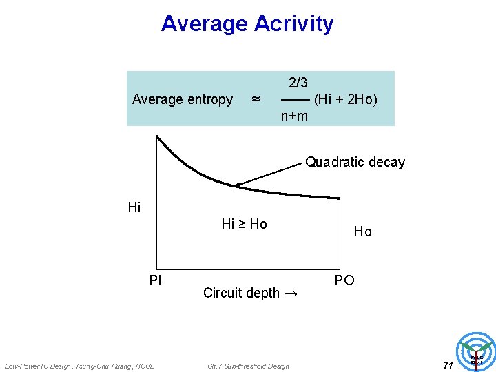
Average Acrivity Average entropy ≈ 2/3 ─── (Hi + 2 Ho) n+m Quadratic decay Hi Hi ≥ Ho PI Low-Power IC Design. Tsung-Chu Huang, NCUE Circuit depth → Ch. 7 Sub-threshold Design Ho PO 71 NCUE EDAT

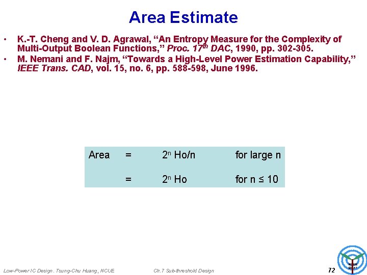
Area Estimate • • K. -T. Cheng and V. D. Agrawal, “An Entropy Measure for the Complexity of Multi-Output Boolean Functions, ” Proc. 17 th DAC, 1990, pp. 302 -305. M. Nemani and F. Najm, “Towards a High-Level Power Estimation Capability, ” IEEE Trans. CAD, vol. 15, no. 6, pp. 588 -598, June 1996. Area Low-Power IC Design. Tsung-Chu Huang, NCUE = 2 n Ho/n for large n = 2 n Ho for n ≤ 10 Ch. 7 Sub-threshold Design 72 NCUE EDAT

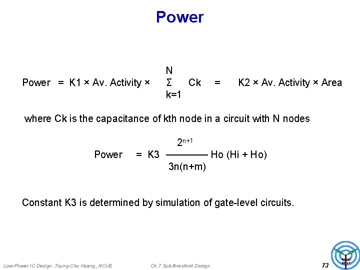
Power = K 1 × Av. Activity × N Σ Ck k=1 = K 2 × Av. Activity × Area where Ck is the capacitance of kth node in a circuit with N nodes Power 2 n+1 = K 3 ────── Ho (Hi + Ho) 3 n(n+m) Constant K 3 is determined by simulation of gate-level circuits. Low-Power IC Design. Tsung-Chu Huang, NCUE Ch. 7 Sub-threshold Design 73 NCUE EDAT

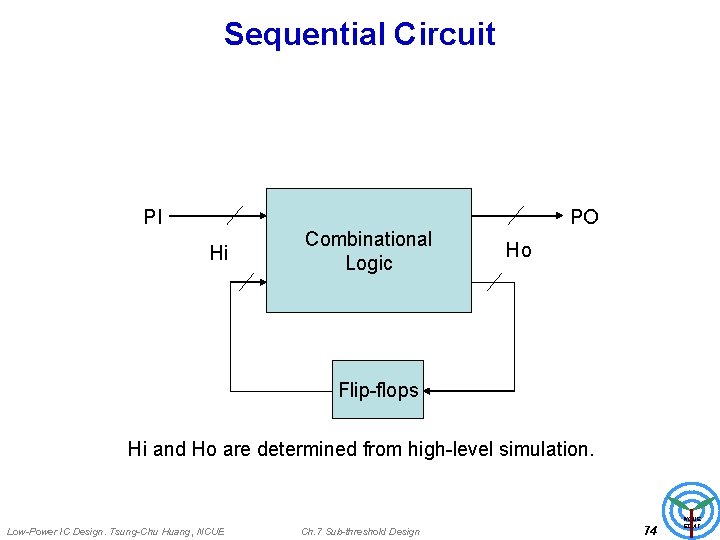
Sequential Circuit PI Hi Combinational Logic PO Ho Flip-flops Hi and Ho are determined from high-level simulation. Low-Power IC Design. Tsung-Chu Huang, NCUE Ch. 7 Sub-threshold Design 74 NCUE EDAT

Empirical Methods • Functional blocks are characterized for power consumption in active and inactive (standby) modes by – Analytical methods, or – Simulation, or – Measurement • A software simulator determined which blocks become active and adds their power consumption. Low-Power IC Design. Tsung-Chu Huang, NCUE Ch. 7 Sub-threshold Design 75 NCUE EDAT

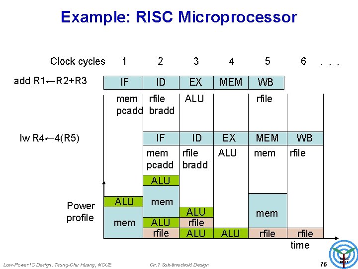
Example: RISC Microprocessor Clock cycles add R 1←R 2+R 3 1 2 3 4 5 IF ID EX MEM WB mem rfile pcadd bradd lw R 4← 4(R 5) IF ALU ID mem rfile pcadd bradd 6 . . . rfile EX MEM ALU mem WB rfile ALU Power profile Low-Power IC Design. Tsung-Chu Huang, NCUE ALU mem ALU rfile ALU Ch. 7 Sub-threshold Design mem ALU rfile time 76 NCUE EDAT

Additional References • P. E. Landman, “A Survey of High-Level Power Estimation Techniques, ” in Low-Power CMOS Design, A. Chandrakasan and R. Brodersen (Editors), New York: IEEE Press, 1998. • P. E. Landman and J. M. Rabaey, “Activity. Sensitive Architectural Power Analysis, ” IEEE Trans. CAD, vol. 15, no. 6, pp. 571 -587, June 1996. Low-Power IC Design. Tsung-Chu Huang, NCUE Ch. 7 Sub-threshold Design 77 NCUE EDAT

Lab 2. Weighted Transition Count • Survey the tools developed by our lab. • Measure the peak power dissipation for some ISCAS 89 benchmark circuit. • Comment how to improve it. Low-Power IC Design. Tsung-Chu Huang, NCUE Ch. 7 Sub-threshold Design 78 NCUE EDAT

Lab 3. Power Estimation using Prime. Power • Generate test patterns for some ISCAS 89 benchmark circuit and execute the logic simulation. • Measure the Average/Peak dissipation • Order the latches and patterns for lowering power dissipation. • Measure the Average/Peak power dissipation again. • Calculate the power reduction. Low-Power IC Design. Tsung-Chu Huang, NCUE Ch. 7 Sub-threshold Design 79 NCUE EDAT