LowPower IC Design Ch 6 LowVoltage Design TsungChu
- Slides: 50

Low-Power IC Design Ch. 6 Low-Voltage Design Tsung-Chu Huang Dep’t of Electronic Eng. , Nat’l Changhua Univ. Spring 2007 Low-Power IC Design. Tsung-Chu Huang, NCUE Ch. 6 Low-Voltage Design 1 NCUE EDAT

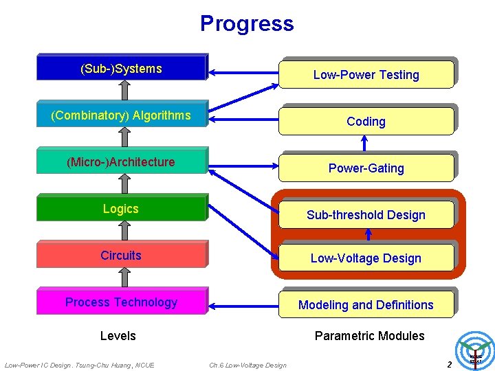
Progress (Sub-)Systems Low-Power Testing (Combinatory) Algorithms Coding (Micro-)Architecture Power-Gating Logics Sub-threshold Design Circuits Low-Voltage Design Process Technology Modeling and Definitions Levels Parametric Modules Low-Power IC Design. Tsung-Chu Huang, NCUE Ch. 6 Low-Voltage Design 2 NCUE EDAT

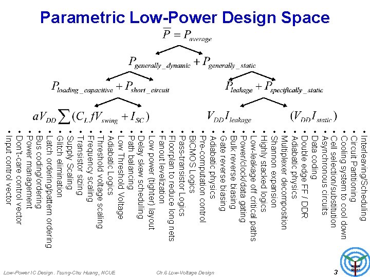
Parametric Low-Power Design Space • Interleaving/Scheduling • Circuit Partitioning • Cooling system to cool down • Cell selection/substitution • Asynchronous circuits • Data coding • Double edge FF / DDR • Adiabatic physics • Multiplexer decomposition • Shannon expansion • Highly stacked logics • Low-leakage off critical paths • Power/clock/data gating • Bulk reverse biasing • Gate reverse biasing • Adiabatic physics • Pre-computation control • Bi. CMOS Logics • Pass-transistor Logics • Floorplan to reduce long nets • Fanout levelization • Low power (tighter) layout • Delay skew scheduling • Path balancing • Low Threshold Voltage • Adiabatic Logics • Threshold voltage scaling • Frequency scaling • Transistor sizing • Supply Scaling • Glitch elimination • Latch ordering/pattern ordering • Bus coding/ordering • Power management • Don’t-care control vector • Input control vector NCUE EDAT 3 Ch. 6 Low-Voltage Design Low-Power IC Design. Tsung-Chu Huang, NCUE

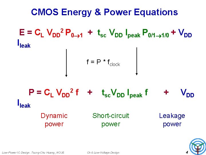
CMOS Energy & Power Equations E = CL VDD 2 P 0 1 + tsc VDD Ipeak P 0/1 1/0 + VDD Ileak f = P * fclock P = CL VDD 2 f Ileak Dynamic power Low-Power IC Design. Tsung-Chu Huang, NCUE + tsc. VDD Ipeak f Short-circuit power Ch. 6 Low-Voltage Design + VDD Leakage power 4 NCUE EDAT

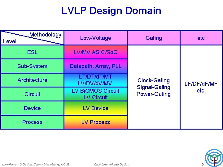
LVLP Design Domain Methodology Low-Voltage Level ESL LV/MV ASIC/So. C Sub-System Datapath, Array, PLL Architecture Circuit LT/DT/d. T/MT LV/DV/d. V/MV LV Bi. CMOS Circuit LV Circuit Device LV Device Process LV Process Low-Power IC Design. Tsung-Chu Huang, NCUE Ch. 6 Low-Voltage Design Gating etc Clock-Gating Signal-Gating Power-Gating LF/DF/d. F/MF etc. 5 NCUE EDAT

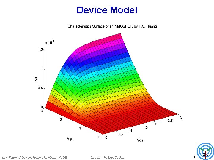
Device Model Low-Power IC Design. Tsung-Chu Huang, NCUE Ch. 6 Low-Voltage Design 7 NCUE EDAT

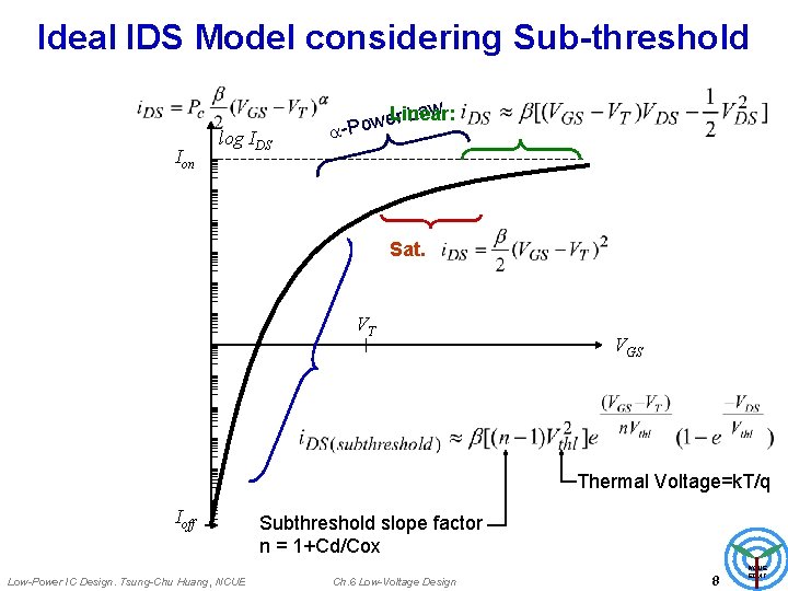
Ideal IDS Model considering Sub-threshold Ion log IDS Linear: Law r e w a-Po Sat. VT VGS Thermal Voltage=k. T/q Ioff Low-Power IC Design. Tsung-Chu Huang, NCUE Subthreshold slope factor n = 1+Cd/Cox Ch. 6 Low-Voltage Design 8 NCUE EDAT

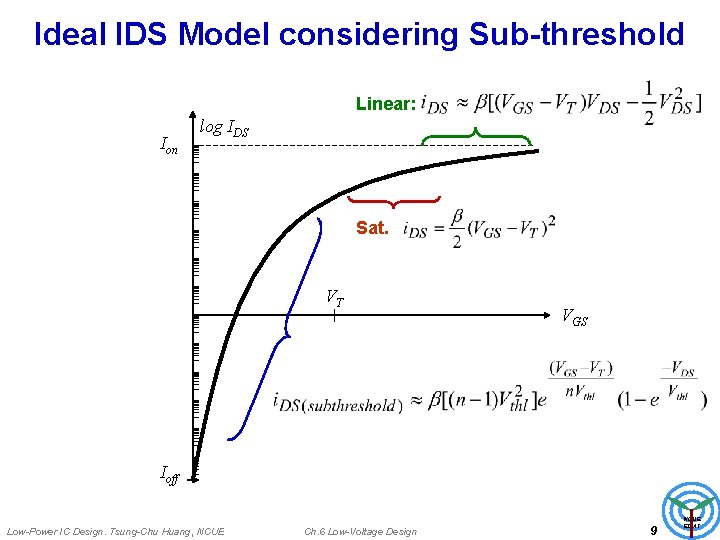
Ideal IDS Model considering Sub-threshold Linear: Ion log IDS Sat. VT VGS Ioff Low-Power IC Design. Tsung-Chu Huang, NCUE Ch. 6 Low-Voltage Design 9 NCUE EDAT

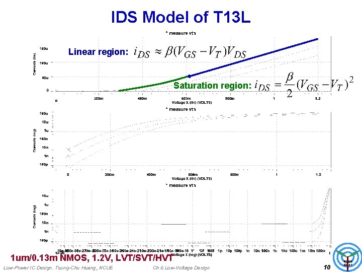
IDS Model of T 13 L Linear region: Saturation region: 1 um/0. 13 m NMOS, 1. 2 V, LVT/SVT/HVT Low-Power IC Design. Tsung-Chu Huang, NCUE Ch. 6 Low-Voltage Design 10 NCUE EDAT

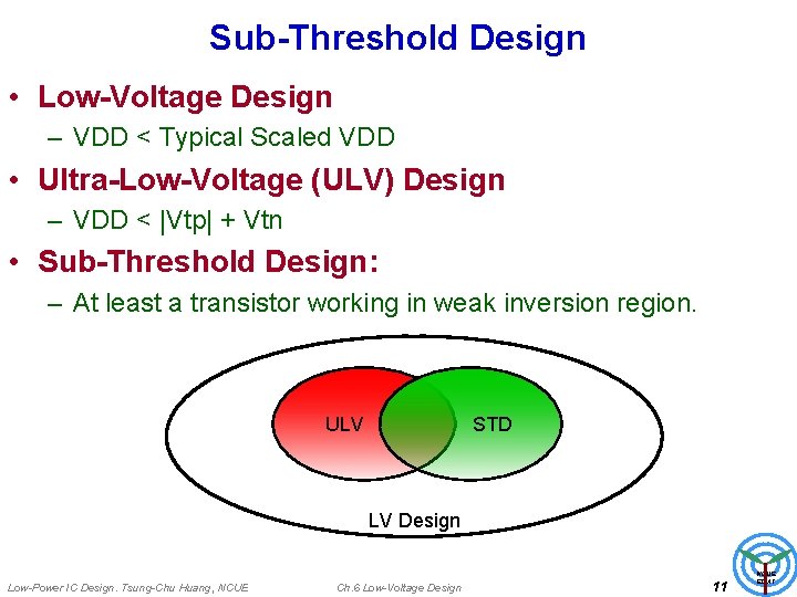
Sub-Threshold Design • Low-Voltage Design – VDD < Typical Scaled VDD • Ultra-Low-Voltage (ULV) Design – VDD < |Vtp| + Vtn • Sub-Threshold Design: – At least a transistor working in weak inversion region. ULV STD LV Design Low-Power IC Design. Tsung-Chu Huang, NCUE Ch. 6 Low-Voltage Design 11 NCUE EDAT

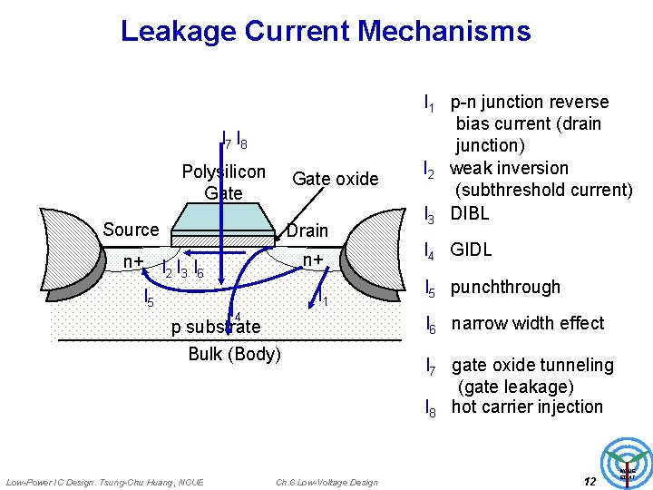
Leakage Current Mechanisms I 7 I 8 Polysilicon Gate oxide Source Drain n+ n+ I I I 2 3 6 I 5 I 1 I 4 p substrate I 4 GIDL I 5 punchthrough I 6 narrow width effect Bulk (Body) Low-Power IC Design. Tsung-Chu Huang, NCUE I 1 p-n junction reverse bias current (drain junction) I 2 weak inversion (subthreshold current) I 3 DIBL Ch. 6 Low-Voltage Design I 7 gate oxide tunneling (gate leakage) I 8 hot carrier injection 12 NCUE EDAT

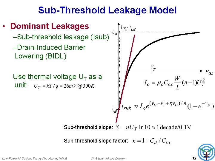
Sub-Threshold Leakage Model • Dominant Leakages –Sub-threshold leakage (Isub) –Drain-Induced Barrier Lowering (BIDL) Ion log IDS VT VGS Use thermal voltage UT as a unit: Ioff Sub-threshold slope: Sub-threshold slope factor: Low-Power IC Design. Tsung-Chu Huang, NCUE Ch. 6 Low-Voltage Design 13 NCUE EDAT

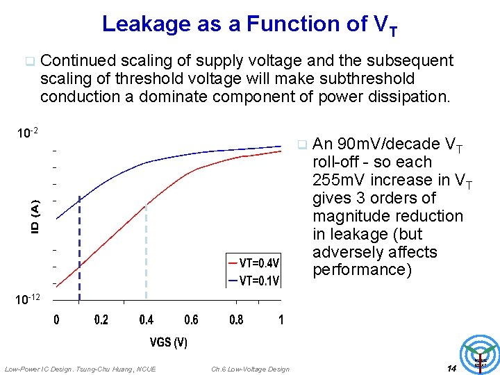
Leakage as a Function of VT q Continued scaling of supply voltage and the subsequent scaling of threshold voltage will make subthreshold conduction a dominate component of power dissipation. 10 -2 q An 90 m. V/decade VT roll-off - so each 255 m. V increase in VT gives 3 orders of magnitude reduction in leakage (but adversely affects performance) 10 -12 Low-Power IC Design. Tsung-Chu Huang, NCUE Ch. 6 Low-Voltage Design 14 NCUE EDAT

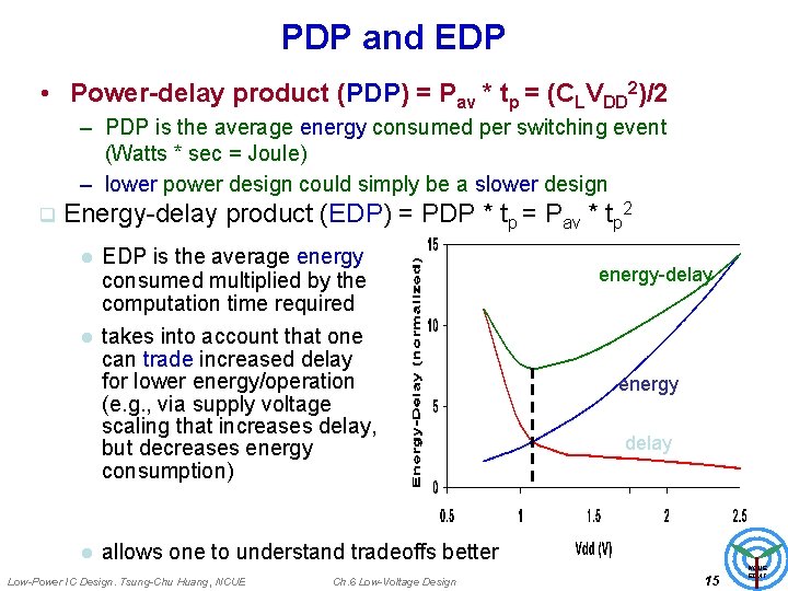
PDP and EDP • Power-delay product (PDP) = Pav * tp = (CLVDD 2)/2 – PDP is the average energy consumed per switching event (Watts * sec = Joule) – lower power design could simply be a slower design q Energy-delay product (EDP) = PDP * tp = Pav * tp 2 l EDP is the average energy consumed multiplied by the computation time required l takes into account that one can trade increased delay for lower energy/operation (e. g. , via supply voltage scaling that increases delay, but decreases energy consumption) l energy-delay energy delay allows one to understand tradeoffs better Low-Power IC Design. Tsung-Chu Huang, NCUE Ch. 6 Low-Voltage Design 15 NCUE EDAT

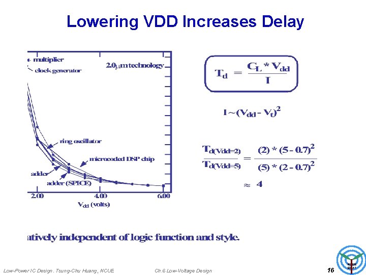
Lowering VDD Increases Delay Low-Power IC Design. Tsung-Chu Huang, NCUE Ch. 6 Low-Voltage Design 16 NCUE EDAT

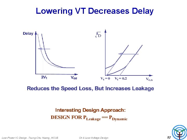
Lowering VT Decreases Delay Low-Power IC Design. Tsung-Chu Huang, NCUE Ch. 6 Low-Voltage Design 17 NCUE EDAT

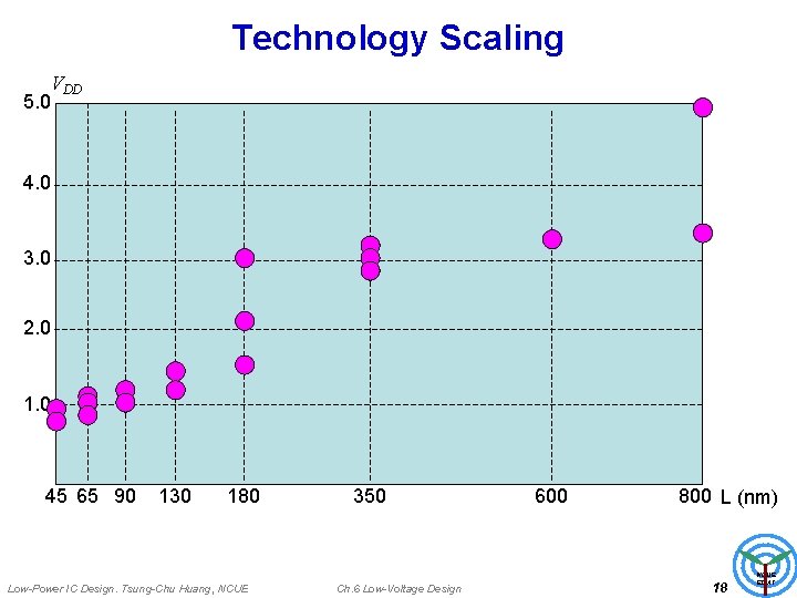
Technology Scaling VDD 5. 0 4. 0 3. 0 2. 0 1. 0 45 65 90 130 180 Low-Power IC Design. Tsung-Chu Huang, NCUE 350 Ch. 6 Low-Voltage Design 600 800 L (nm) 18 NCUE EDAT

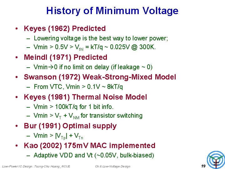
History of Minimum Voltage • Keyes (1962) Predicted – Lowering voltage is the best way to lower power; – Vmin > 0. 5 V > Vthl = k. T/q ~ 0. 025 V @ 300 K. • Meindl (1971) Predicted – Vmin 0 if no limit on delay (if leakage ~ 0) • Swanson (1972) Weak-Strong-Mixed Model – From VTC, Vmin > 0. 1 V ~ 8 k. T/q • Keyes (1981) Thermal Noise Model – Vmin > 100 k. T/q for 1 bit info. – Vmin > VT + VNM for transistor switching • Bur (1991) Optimal supply – Vmin > |VTp| + VTn • Kao (2002) 175 m. V MAC implemented – Adaptive VDD and Vt (~0. 05 V, bulk-biased) Low-Power IC Design. Tsung-Chu Huang, NCUE Ch. 6 Low-Voltage Design 19 NCUE EDAT

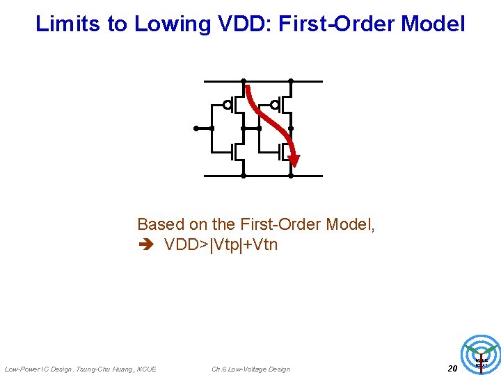
Limits to Lowing VDD: First-Order Model Based on the First-Order Model, VDD>|Vtp|+Vtn Low-Power IC Design. Tsung-Chu Huang, NCUE Ch. 6 Low-Voltage Design 20 NCUE EDAT

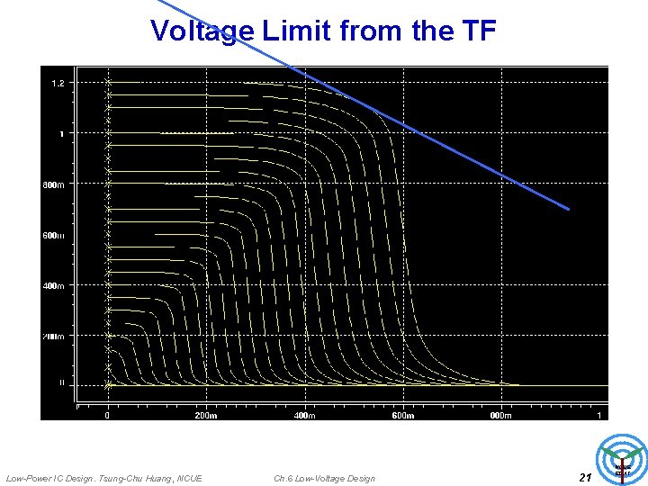
Voltage Limit from the TF Low-Power IC Design. Tsung-Chu Huang, NCUE Ch. 6 Low-Voltage Design 21 NCUE EDAT

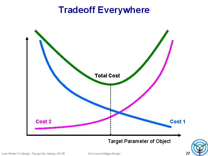
Tradeoff Everywhere Total Cost 2 Cost 1 Target Parameter of Object Low-Power IC Design. Tsung-Chu Huang, NCUE Ch. 6 Low-Voltage Design 22 NCUE EDAT

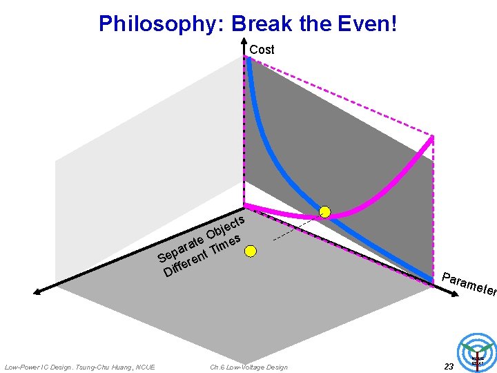
Philosophy: Break the Even! Cost cts e j b O e es t a m r i T pa Se erent f Dif Low-Power IC Design. Tsung-Chu Huang, NCUE Ch. 6 Low-Voltage Design Para 23 mete r NCUE EDAT

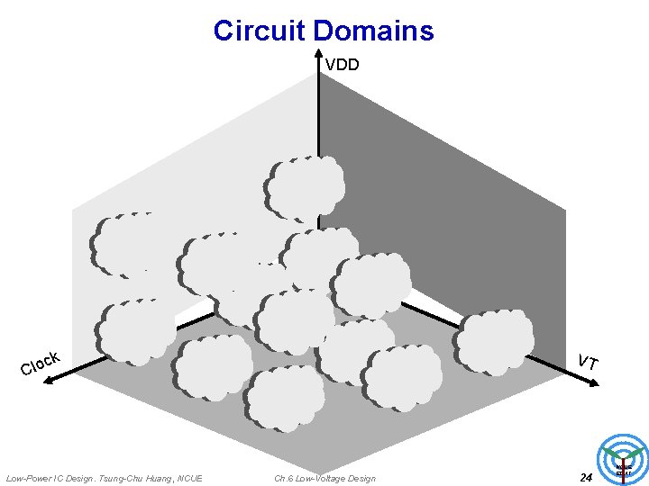
Circuit Domains VDD k VT c Clo Low-Power IC Design. Tsung-Chu Huang, NCUE Ch. 6 Low-Voltage Design 24 NCUE EDAT

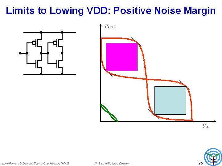
Limits to Lowing VDD: Positive Noise Margin Vout Vin Low-Power IC Design. Tsung-Chu Huang, NCUE Ch. 6 Low-Voltage Design 25 NCUE EDAT

Voltage Islands Low-Power IC Design. Tsung-Chu Huang, NCUE Ch. 6 Low-Voltage Design 26 NCUE EDAT

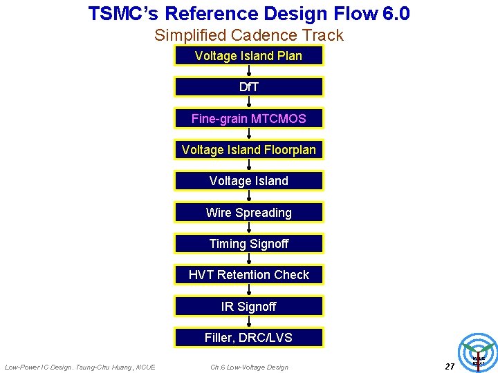
TSMC’s Reference Design Flow 6. 0 Simplified Cadence Track Voltage Island Plan Df. T Fine-grain MTCMOS Voltage Island Floorplan Voltage Island Wire Spreading Timing Signoff HVT Retention Check IR Signoff Filler, DRC/LVS Low-Power IC Design. Tsung-Chu Huang, NCUE Ch. 6 Low-Voltage Design 27 NCUE EDAT

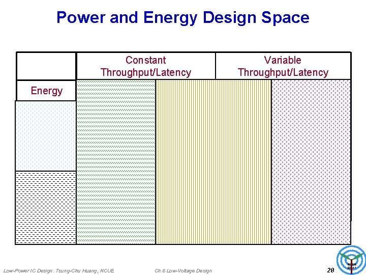
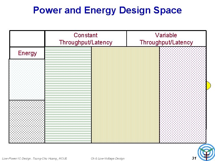
Power and Energy Design Space Constant Throughput/Latency Energy Design Time Active (Dynamic) Leakage (Standby) Variable Throughput/Latency Non-active Modules Run Time Logic design Reduced Vdd TSizing Multi-Vdd Clock Gating DFS, DVS (Dynamic Freq, Voltage Scaling) Multi-VT Stack effect Pin ordering Sleep Transistors Multi-Vdd Variable VT Input control Variable VT Low-Power IC Design. Tsung-Chu Huang, NCUE Ch. 6 Low-Voltage Design 28 NCUE EDAT

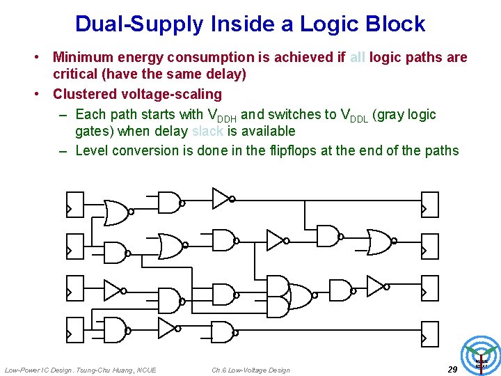
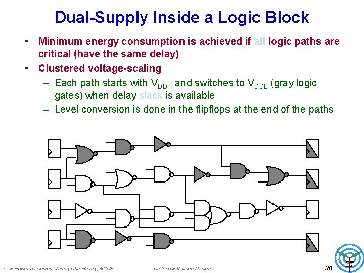
Dual-Supply Inside a Logic Block • Minimum energy consumption is achieved if all logic paths are critical (have the same delay) • Clustered voltage-scaling – Each path starts with VDDH and switches to VDDL (gray logic gates) when delay slack is available – Level conversion is done in the flipflops at the end of the paths Low-Power IC Design. Tsung-Chu Huang, NCUE Ch. 6 Low-Voltage Design 29 NCUE EDAT

Dual-Supply Inside a Logic Block • Minimum energy consumption is achieved if all logic paths are critical (have the same delay) • Clustered voltage-scaling – Each path starts with VDDH and switches to VDDL (gray logic gates) when delay slack is available – Level conversion is done in the flipflops at the end of the paths Low-Power IC Design. Tsung-Chu Huang, NCUE Ch. 6 Low-Voltage Design 30 NCUE EDAT

Power and Energy Design Space Constant Throughput/Latency Energy Design Time Active (Dynamic) Leakage (Standby) Variable Throughput/Latency Non-active Modules Run Time Logic design Reduced Vdd TSizing Multi-Vdd Clock Gating DFS, DVS (Dynamic Freq, Voltage Scaling) Multi-VT Stack effect Pin ordering Sleep Transistors Multi-Vdd Variable VT Input control Variable VT Low-Power IC Design. Tsung-Chu Huang, NCUE Ch. 6 Low-Voltage Design 31 NCUE EDAT

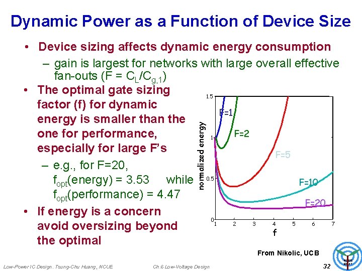
Dynamic Power as a Function of Device Size normalized energy • Device sizing affects dynamic energy consumption – gain is largest for networks with large overall effective fan-outs (F = CL/Cg, 1) • The optimal gate sizing 1. 5 factor (f) for dynamic F=1 energy is smaller than the F=2 one for performance, 1 especially for large F’s F=5 – e. g. , for F=20, fopt(energy) = 3. 53 while 0. 5 F=10 fopt(performance) = 4. 47 F=20 • If energy is a concern 0 1 2 3 4 5 6 7 avoid oversizing beyond f the optimal From Nikolic, UCB Low-Power IC Design. Tsung-Chu Huang, NCUE Ch. 6 Low-Voltage Design 32 NCUE EDAT

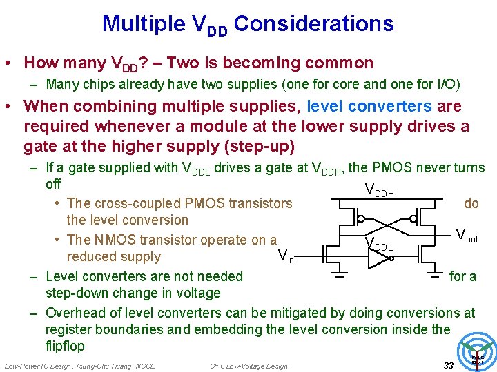
Multiple VDD Considerations • How many VDD? – Two is becoming common – Many chips already have two supplies (one for core and one for I/O) • When combining multiple supplies, level converters are required whenever a module at the lower supply drives a gate at the higher supply (step-up) – If a gate supplied with VDDL drives a gate at VDDH, the PMOS never turns off VDDH • The cross-coupled PMOS transistors do the level conversion Vout • The NMOS transistor operate on a VDDL Vin reduced supply – Level converters are not needed for a step-down change in voltage – Overhead of level converters can be mitigated by doing conversions at register boundaries and embedding the level conversion inside the flipflop Low-Power IC Design. Tsung-Chu Huang, NCUE Ch. 6 Low-Voltage Design 33 NCUE EDAT

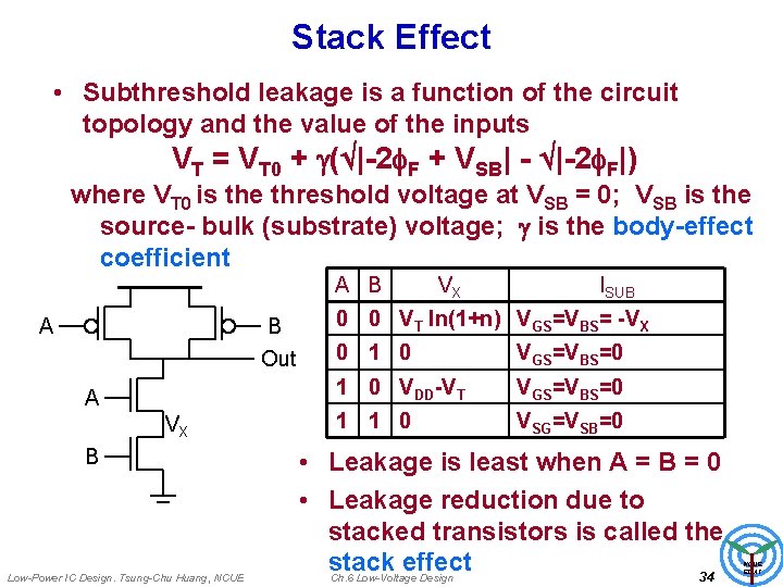
Stack Effect • Subthreshold leakage is a function of the circuit topology and the value of the inputs VT = VT 0 + ( |-2 F + VSB| - |-2 F|) where VT 0 is the threshold voltage at VSB = 0; VSB is the source- bulk (substrate) voltage; is the body-effect coefficient A B Out A VX B Low-Power IC Design. Tsung-Chu Huang, NCUE VX ISUB 0 0 VT ln(1+n) VGS=VBS= -VX 0 1 0 VGS=VBS=0 1 0 VDD-VT VGS=VBS=0 1 1 0 VSG=VSB=0 • Leakage is least when A = B = 0 • Leakage reduction due to stacked transistors is called the stack effect Ch. 6 Low-Voltage Design 34 NCUE EDAT

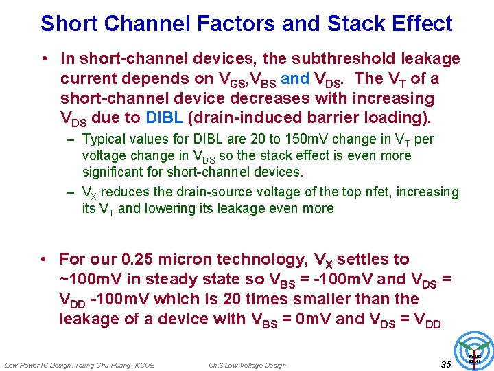
Short Channel Factors and Stack Effect • In short-channel devices, the subthreshold leakage current depends on VGS, VBS and VDS. The VT of a short-channel device decreases with increasing VDS due to DIBL (drain-induced barrier loading). – Typical values for DIBL are 20 to 150 m. V change in VT per voltage change in VDS so the stack effect is even more significant for short-channel devices. – VX reduces the drain-source voltage of the top nfet, increasing its VT and lowering its leakage even more • For our 0. 25 micron technology, VX settles to ~100 m. V in steady state so VBS = -100 m. V and VDS = VDD -100 m. V which is 20 times smaller than the leakage of a device with VBS = 0 m. V and VDS = VDD Low-Power IC Design. Tsung-Chu Huang, NCUE Ch. 6 Low-Voltage Design 35 NCUE EDAT

Dynamic Frequency and Voltage Scaling • Intel’s Speed. Step – Hardware that steps down the clock frequency (dynamic frequency scaling – DFS) when the user unplugs from AC power • PLL from 650 MHz 500 MHz – CPU stalls during Speed. Step adjustment • Transmeta Long. Run – Hardware that applies both DFS and DVS (dynamic supply voltage scaling) • 32 levels of VDD from 1. 1 V to 1. 6 V • PLL from 200 MHz 700 MHz in increments of 33 MHz – Triggered when CPU load change is detected by software • heavier load ramp up VDD, when stable speed up clock • lighter load slow down clock, when PLL locks onto new rate, ramp down VDD – CPU stalls only during PLL relock (< 20 microsec) Low-Power IC Design. Tsung-Chu Huang, NCUE Ch. 6 Low-Voltage Design 36 NCUE EDAT

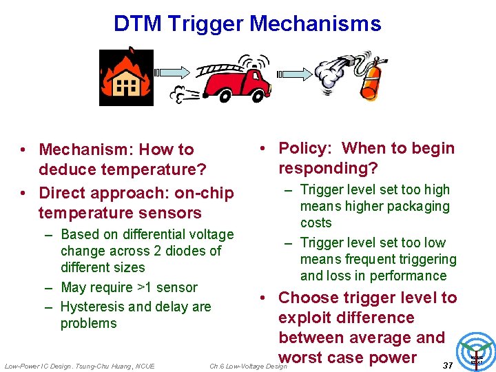
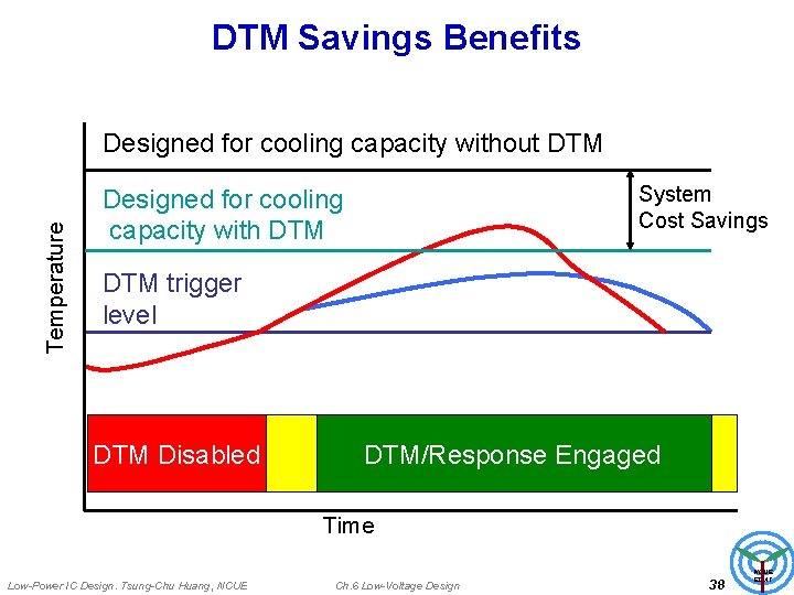
DTM Trigger Mechanisms • Mechanism: How to deduce temperature? • Direct approach: on-chip temperature sensors – Based on differential voltage change across 2 diodes of different sizes – May require >1 sensor – Hysteresis and delay are problems Low-Power IC Design. Tsung-Chu Huang, NCUE • Policy: When to begin responding? – Trigger level set too high means higher packaging costs – Trigger level set too low means frequent triggering and loss in performance • Choose trigger level to exploit difference between average and worst case power Ch. 6 Low-Voltage Design 37 NCUE EDAT

DTM Savings Benefits Temperature Designed for cooling capacity without DTM System Cost Savings Designed for cooling capacity with DTM trigger level DTM Disabled DTM/Response Engaged Time Low-Power IC Design. Tsung-Chu Huang, NCUE Ch. 6 Low-Voltage Design 38 NCUE EDAT

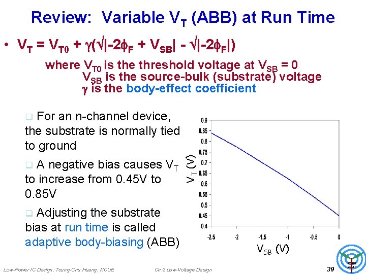
Review: Variable VT (ABB) at Run Time • VT = VT 0 + ( |-2 F + VSB| - |-2 F|) where VT 0 is the threshold voltage at VSB = 0 VSB is the source-bulk (substrate) voltage is the body-effect coefficient For an n-channel device, the substrate is normally tied to ground A negative bias causes VT to increase from 0. 45 V to 0. 85 V q VT (V) q Adjusting the substrate bias at run time is called adaptive body-biasing (ABB) q Low-Power IC Design. Tsung-Chu Huang, NCUE Ch. 6 Low-Voltage Design VSB (V) 39 NCUE EDAT

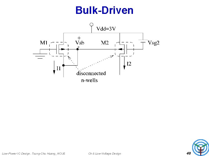
Bulk-Driven Low-Power IC Design. Tsung-Chu Huang, NCUE Ch. 6 Low-Voltage Design 40 NCUE EDAT

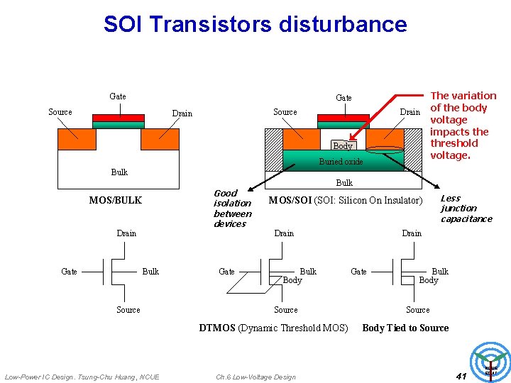
SOI Transistors disturbance Gate Source Drain Body Buried oxide The variation of the body voltage impacts the threshold voltage. Bulk MOS/BULK Drain Gate Bulk Source Good isolation between devices Gate Bulk MOS/SOI (SOI: Silicon On Insulator) Drain Bulk Body Source DTMOS (Dynamic Threshold MOS) Low-Power IC Design. Tsung-Chu Huang, NCUE Ch. 6 Low-Voltage Design Less junction capacitance Drain Gate Bulk Body Source Body Tied to Source 41 NCUE EDAT

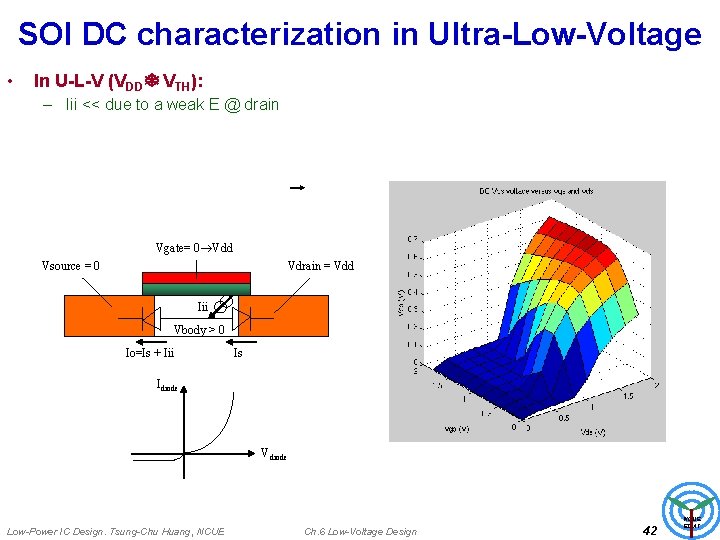
SOI DC characterization in Ultra-Low-Voltage • In U-L-V (VDD VTH): – Iii << due to a weak E @ drain Vgate= 0 Vdd Vsource = 0 Vdrain = Vdd Iii Vbody > 0 Io=Is + Iii Is Idiode Vdiode Low-Power IC Design. Tsung-Chu Huang, NCUE Ch. 6 Low-Voltage Design 42 NCUE EDAT

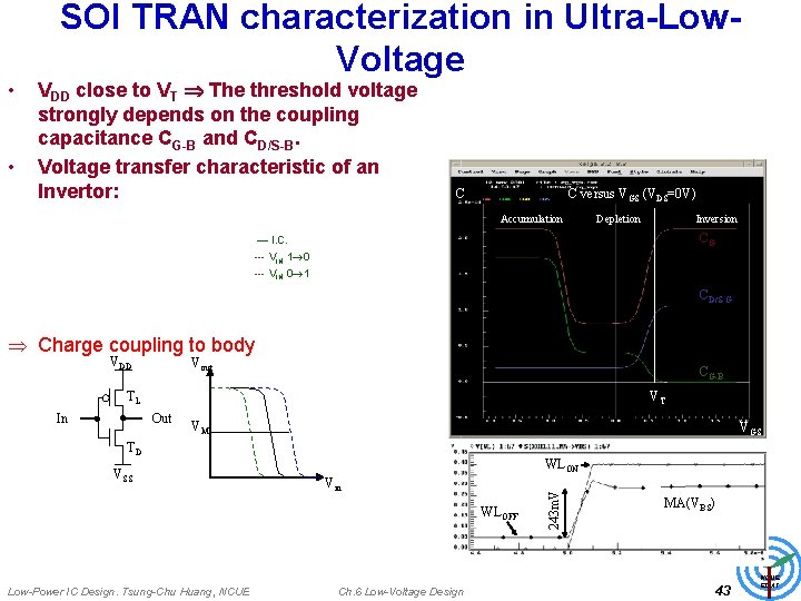
• • SOI TRAN characterization in Ultra-Low. Voltage VDD close to VT The threshold voltage strongly depends on the coupling capacitance CG-B and CD/S-B. Voltage transfer characteristic of an Invertor: C versus VGS (VDS=0 V) C Accumulation Depletion Inversion CG — I. C. --- VIN 1 0 --- VIN 0 1 CD/S-G Charge coupling to body VDD Vout CG-B TL Out VM VGS TD VSS WLON Vin WLOFF Low-Power IC Design. Tsung-Chu Huang, NCUE Ch. 6 Low-Voltage Design 243 m. V In VT MA(VBS) 43 NCUE EDAT

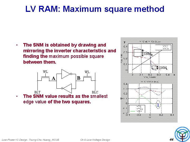
LV RAM: Maximum square method • y The SNM is obtained by drawing and mirroring the inverter characteristics and finding the maximum possible square between them. SNMH SNML WL WL • BLT B BLC The SNM value results as the smallest edge value of the two squares. Low-Power IC Design. Tsung-Chu Huang, NCUE Ch. 6 Low-Voltage Design V A x 44 NCUE EDAT

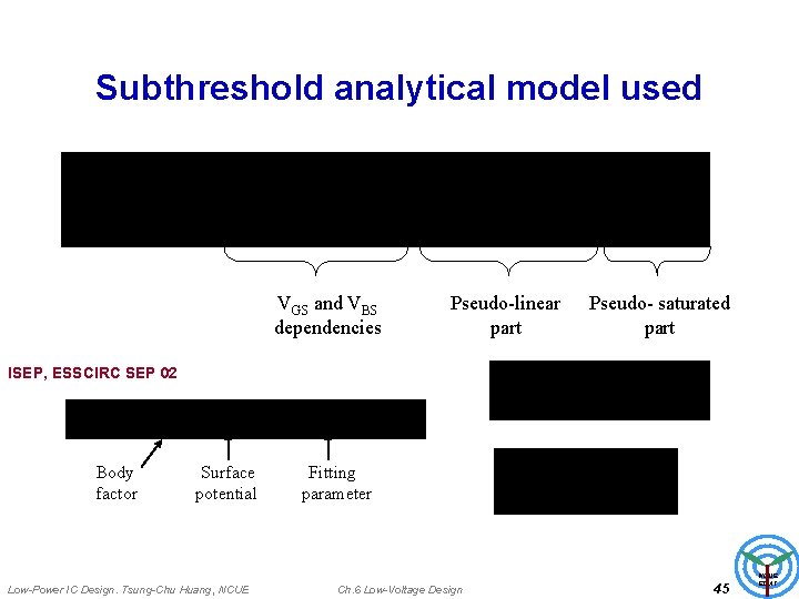
Subthreshold analytical model used VGS and VBS dependencies Pseudo-linear part Pseudo- saturated part ISEP, ESSCIRC SEP 02 Body factor Surface potential Low-Power IC Design. Tsung-Chu Huang, NCUE Fitting parameter Ch. 6 Low-Voltage Design 45 NCUE EDAT

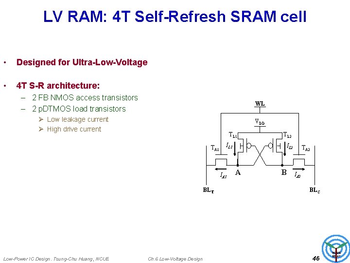
LV RAM: 4 T Self-Refresh SRAM cell • Designed for Ultra-Low-Voltage • 4 T S-R architecture: – 2 FB NMOS access transistors – 2 p. DTMOS load transistors WL Ø Low leakage current Ø High drive current VDD TL 1 TA 1 IL 1 IA 1 BLT Low-Power IC Design. Tsung-Chu Huang, NCUE Ch. 6 Low-Voltage Design TL 2 IL 2 A B TA 2 IA 2 BLC 46 NCUE EDAT

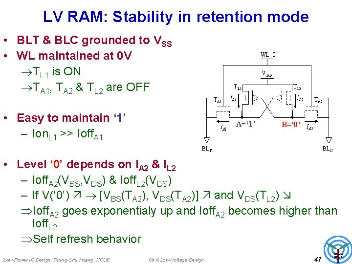
LV RAM: Stability in retention mode • BLT & BLC grounded to VSS • WL maintained at 0 V TL 1 is ON TA 1, TA 2 & TL 2 are OFF WL=0 VDD TL 1 TA 1 • Easy to maintain ‘ 1’ – Ion. L 1 >> Ioff. A 1 IL 1 A=‘ 1’ TL 2 IL 2 B=‘ 0’ TA 2 IA 2 BLT BLC • Level ‘ 0’ depends on IA 2 & IL 2 – Ioff. A 2(VBS, VDS) & Ioff. L 2(VDS) – If V(‘ 0’) [VBS(TA 2), VDS(TA 2)] and VDS(TL 2) Ioff. A 2 goes exponentialy up and Ioff. A 2 becomes higher than Ioff. L 2 Self refresh behavior Low-Power IC Design. Tsung-Chu Huang, NCUE Ch. 6 Low-Voltage Design 47 NCUE EDAT

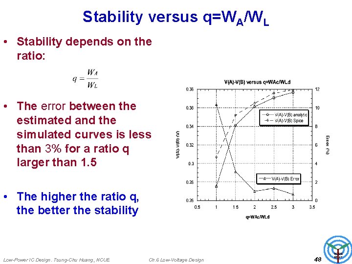
Stability versus q=WA/WL • Stability depends on the ratio: • The error between the estimated and the simulated curves is less than 3% for a ratio q larger than 1. 5 • The higher the ratio q, the better the stability Low-Power IC Design. Tsung-Chu Huang, NCUE Ch. 6 Low-Voltage Design 48 NCUE EDAT

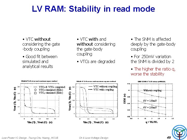
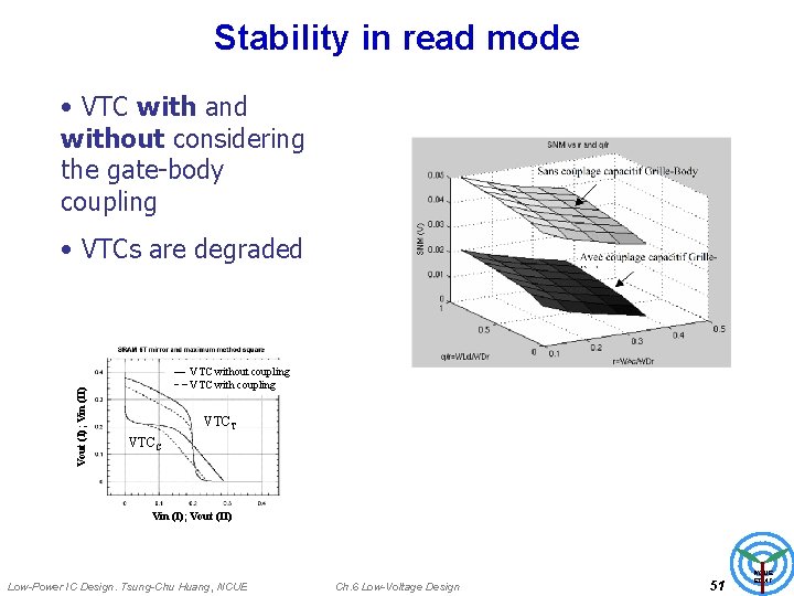
LV RAM: Stability in read mode • VTC without considering the gate -body coupling • VTC with and without considering the gate-body coupling Vin (T) ; Vout (C) (v) Low-Power IC Design. Tsung-Chu Huang, NCUE • The higher the ratio q, worse the stability VTC without coupling VTC with coupling Without coupling SNM (v) VTCT & VTCC computed VTCT simulated (Eldo) VTCC simulated (Eldo) • For 250 m. V variation the SNM is divided by 2 • VTCs are degraded Vout (T), Vin (C) (v) • Good fit between simulated analytical results • The SNM is affected deeply by the gate-body coupling DV = 150 m. V DV = 250 m. V Vin (T) ; Vout (C) (v) Ch. 6 Low-Voltage Design q = WA/WL 49 NCUE EDAT

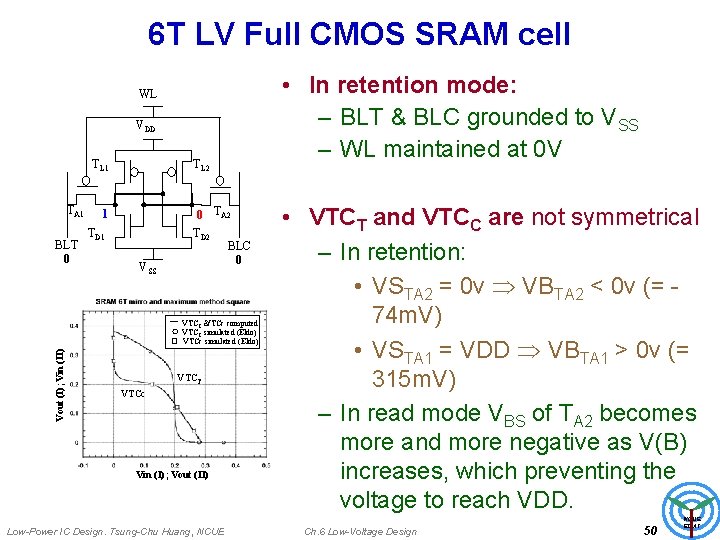
6 T LV Full CMOS SRAM cell • In retention mode: – BLT & BLC grounded to VSS – WL maintained at 0 V WL VDD TL 1 TA 1 BLT 0 TL 2 0 TA 2 1 TD 2 VSS BLC 0 Vout (I); Vin (II) VTCT & VTCc computed VTCT simulated (Eldo) VTCc simulated (Eldo) VTCT VTCc Vin (I); Vout (II) Low-Power IC Design. Tsung-Chu Huang, NCUE • VTCT and VTCC are not symmetrical – In retention: • VSTA 2 = 0 v VBTA 2 < 0 v (= 74 m. V) • VSTA 1 = VDD VBTA 1 > 0 v (= 315 m. V) – In read mode VBS of TA 2 becomes more and more negative as V(B) increases, which preventing the voltage to reach VDD. Ch. 6 Low-Voltage Design 50 NCUE EDAT

Stability in read mode • VTC with and without considering the gate-body coupling Vout (I); Vin (II) • VTCs are degraded VTC without coupling VTC with coupling VTCT VTCC Vin (I); Vout (II) Low-Power IC Design. Tsung-Chu Huang, NCUE Ch. 6 Low-Voltage Design 51 NCUE EDAT