LowPower IC Design Ch 3 Process Technology TsungChu
- Slides: 16

Low-Power IC Design Ch. 3 Process Technology Tsung-Chu Huang Dep’t of Electronic Eng. , Nat’l Changhua Univ. Spring 2007 Low-Power IC Design. Tsung-Chu Huang, NCUE Ch. 3 Process Technology 1 NCUE EDAT

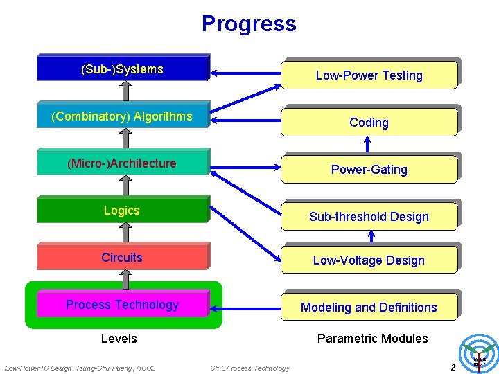
Progress (Sub-)Systems Low-Power Testing (Combinatory) Algorithms Coding (Micro-)Architecture Power-Gating Logics Sub-threshold Design Circuits Low-Voltage Design Process Technology Modeling and Definitions Levels Parametric Modules Low-Power IC Design. Tsung-Chu Huang, NCUE Ch. 3 Process Technology 2 NCUE EDAT

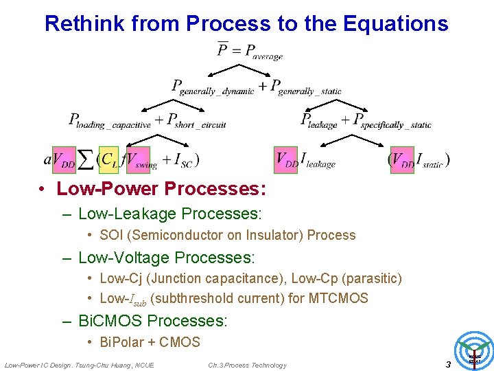
Rethink from Process to the Equations • Low-Power Processes: – Low-Leakage Processes: • SOI (Semiconductor on Insulator) Process – Low-Voltage Processes: • Low-Cj (Junction capacitance), Low-Cp (parasitic) • Low-Isub (subthreshold current) for MTCMOS – Bi. CMOS Processes: • Bi. Polar + CMOS Low-Power IC Design. Tsung-Chu Huang, NCUE Ch. 3 Process Technology 3 NCUE EDAT

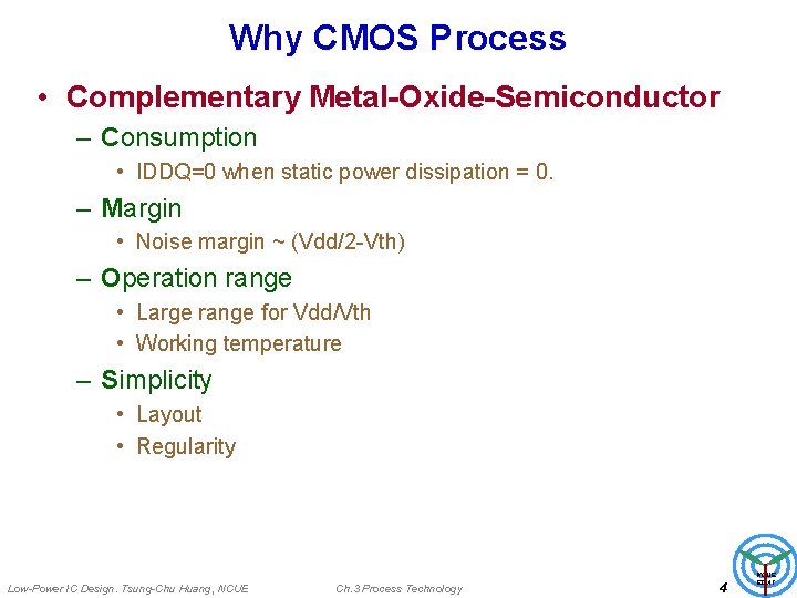
Why CMOS Process • Complementary Metal-Oxide-Semiconductor – Consumption • IDDQ=0 when static power dissipation = 0. – Margin • Noise margin ~ (Vdd/2 -Vth) – Operation range • Large range for Vdd/Vth • Working temperature – Simplicity • Layout • Regularity Low-Power IC Design. Tsung-Chu Huang, NCUE Ch. 3 Process Technology 4 NCUE EDAT

Reviews on Typical CMOS Process • Chapter 2 in “Introduction to VLSI Design” – Click here from website http: //163. 223. 30/tch/lecture/VLSIDesign 2006/VLSI 02. ppt – Click here from the file in the current directory. Low-Power IC Design. Tsung-Chu Huang, NCUE Ch. 3 Process Technology 5 NCUE EDAT

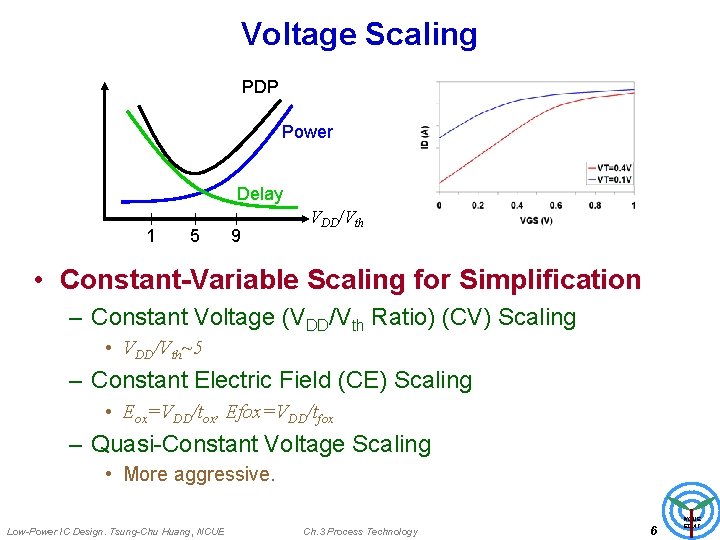
Voltage Scaling PDP Power Delay 1 5 9 VDD/Vth • Constant-Variable Scaling for Simplification – Constant Voltage (VDD/Vth Ratio) (CV) Scaling • VDD/Vth~5 – Constant Electric Field (CE) Scaling • Eox=VDD/tox, Efox=VDD/tfox – Quasi-Constant Voltage Scaling • More aggressive. Low-Power IC Design. Tsung-Chu Huang, NCUE Ch. 3 Process Technology 6 NCUE EDAT

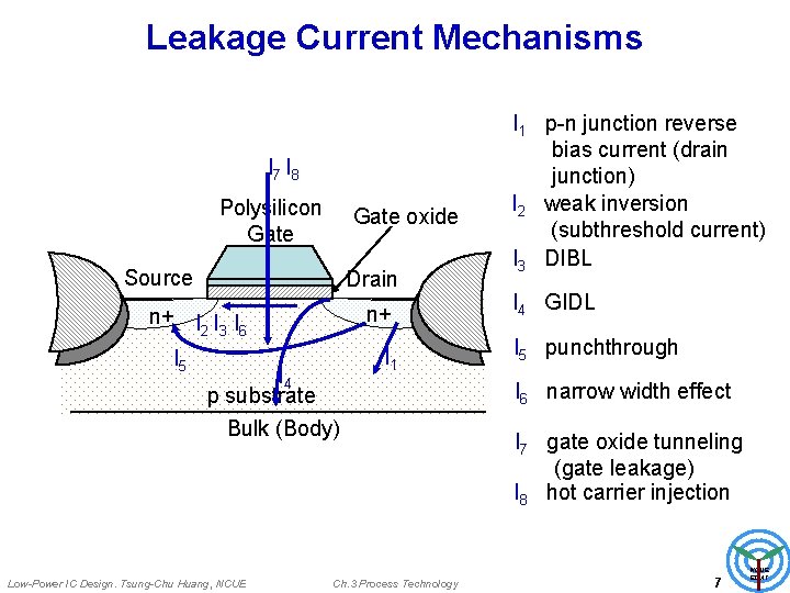
Leakage Current Mechanisms I 7 I 8 Polysilicon Gate oxide Source Drain n+ n+ I I I 2 3 6 I 5 I 1 I 4 p substrate I 4 GIDL I 5 punchthrough I 6 narrow width effect Bulk (Body) Low-Power IC Design. Tsung-Chu Huang, NCUE I 1 p-n junction reverse bias current (drain junction) I 2 weak inversion (subthreshold current) I 3 DIBL Ch. 3 Process Technology I 7 gate oxide tunneling (gate leakage) I 8 hot carrier injection 7 NCUE EDAT

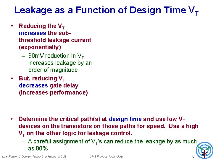
Leakage as a Function of Design Time VT • Reducing the VT increases the subthreshold leakage current (exponentially) – 90 m. V reduction in VT increases leakage by an order of magnitude • But, reducing VT decreases gate delay (increases performance) • Determine the critical path(s) at design time and use low VT devices on the transistors on those paths for speed. Use a high VT on the other logic for leakage control. – A careful assignment of VT’s can reduce the leakage by as much as 80% Low-Power IC Design. Tsung-Chu Huang, NCUE Ch. 3 Process Technology 8 NCUE EDAT

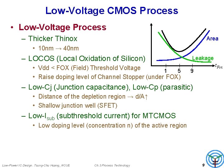
Low-Voltage CMOS Process • Low-Voltage Process – Thicker Thinox Area • 10 nm → 40 nm – LOCOS (Local Oxidation of Silicon) • Vdd < FOX (Field) Threshold Voltage 1 5 • Raise doping level of Channel Stopper (under FOX) Leakage t. Fox 9 – Low-Cj (Junction capacitance), Low-Cp (parasitic) • Distance of the depletion region → d/A↑ • Shallow junction well (SFET) – Low-Isub (subthreshold current) for MTCMOS • Low doping level (concentration n) of the active region Low-Power IC Design. Tsung-Chu Huang, NCUE Ch. 3 Process Technology 9 NCUE EDAT

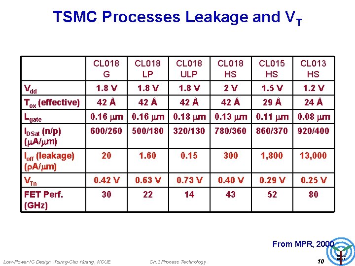
TSMC Processes Leakage and VT CL 018 G CL 018 LP CL 018 ULP CL 018 HS CL 015 HS CL 013 HS Vdd 1. 8 V 2 V 1. 5 V 1. 2 V Tox (effective) 42 Å 29 Å 24 Å Lgate 0. 16 m 0. 18 m 0. 13 m 0. 11 m 0. 08 m IDSat (n/p) ( A/ m) 600/260 500/180 320/130 780/360 860/370 920/400 20 1. 60 0. 15 300 1, 800 13, 000 0. 42 V 0. 63 V 0. 73 V 0. 40 V 0. 29 V 0. 25 V 30 22 14 43 52 80 Ioff (leakage) ( A/ m) VTn FET Perf. (GHz) From MPR, 2000 Low-Power IC Design. Tsung-Chu Huang, NCUE Ch. 3 Process Technology 10 NCUE EDAT

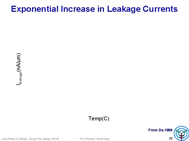
Ileakage(n. A/ m) Exponential Increase in Leakage Currents Temp(C) From De, 1999 Low-Power IC Design. Tsung-Chu Huang, NCUE Ch. 3 Process Technology 11 NCUE EDAT

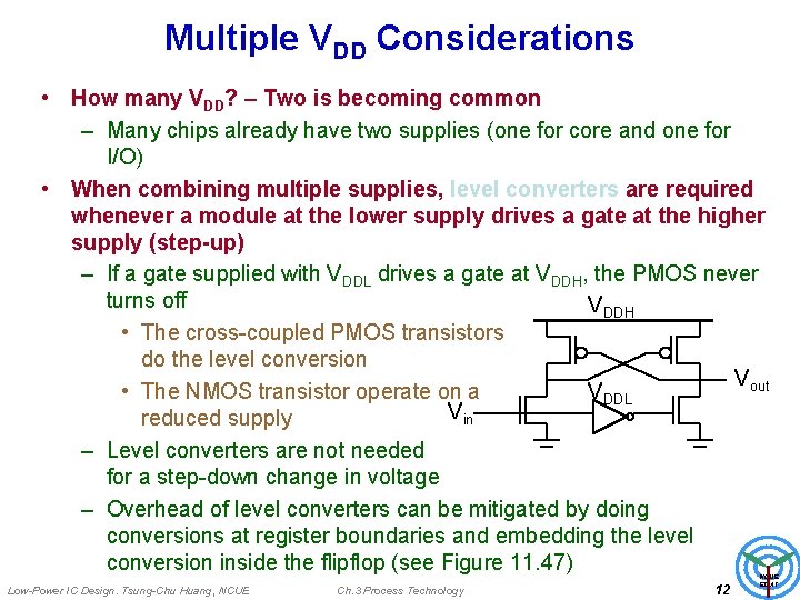
Multiple VDD Considerations • How many VDD? – Two is becoming common – Many chips already have two supplies (one for core and one for I/O) • When combining multiple supplies, level converters are required whenever a module at the lower supply drives a gate at the higher supply (step-up) – If a gate supplied with VDDL drives a gate at VDDH, the PMOS never turns off VDDH • The cross-coupled PMOS transistors do the level conversion Vout • The NMOS transistor operate on a VDDL Vin reduced supply – Level converters are not needed for a step-down change in voltage – Overhead of level converters can be mitigated by doing conversions at register boundaries and embedding the level conversion inside the flipflop (see Figure 11. 47) Low-Power IC Design. Tsung-Chu Huang, NCUE Ch. 3 Process Technology 12 NCUE EDAT

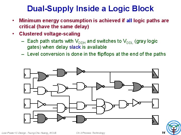
Dual-Supply Inside a Logic Block • Minimum energy consumption is achieved if all logic paths are critical (have the same delay) • Clustered voltage-scaling – Each path starts with VDDH and switches to VDDL (gray logic gates) when delay slack is available – Level conversion is done in the flipflops at the end of the paths Low-Power IC Design. Tsung-Chu Huang, NCUE Ch. 3 Process Technology 14 NCUE EDAT

Short Channel Factors and Stack Effect • In short-channel devices, the subthreshold leakage current depends on VGS, VBS and VDS. The VT of a short-channel device decreases with increasing VDS due to DIBL (drain-induced barrier loading). – Typical values for DIBL are 20 to 150 m. V change in VT per voltage change in VDS so the stack effect is even more significant for short-channel devices. – VX reduces the drain-source voltage of the top nfet, increasing its VT and lowering its leakage even more • For our 0. 25 micron technology, VX settles to ~100 m. V in steady state so VBS = -100 m. V and VDS = VDD -100 m. V which is 20 times smaller than the leakage of a device with VBS = 0 m. V and VDS = VDD Low-Power IC Design. Tsung-Chu Huang, NCUE Ch. 3 Process Technology 15 NCUE EDAT

Simplified Typical Bipolar Process • BJT (Bipolar-Junction Transistor) – Q 1 C B E A=area of Collector – Click Here for Addendum File, Process 1 – Click Here for Addendum File, Process 2 Low-Power IC Design. Tsung-Chu Huang, NCUE Ch. 3 Process Technology 16 NCUE EDAT

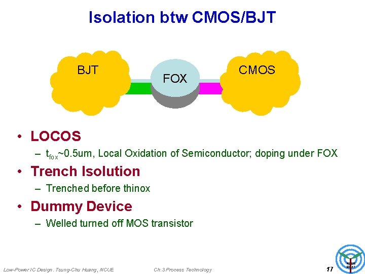
Isolation btw CMOS/BJT FOX CMOS • LOCOS – tfox~0. 5 um, Local Oxidation of Semiconductor; doping under FOX • Trench Isolution – Trenched before thinox • Dummy Device – Welled turned off MOS transistor Low-Power IC Design. Tsung-Chu Huang, NCUE Ch. 3 Process Technology 17 NCUE EDAT