CHAPTER 4 IMPERFECTIONS IN SOLIDS ISSUES TO ADDRESS

- Slides: 81

CHAPTER 4: IMPERFECTIONS IN SOLIDS ISSUES TO ADDRESS. . . • What are the solidification mechanisms? • What types of defects arise in solids? • How do defects affect material properties? • Are defects undesirable? Chapter 4 - 1

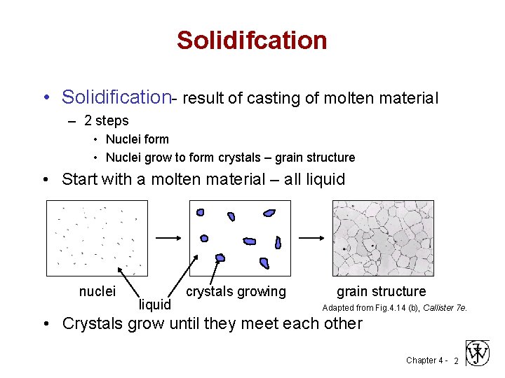
Solidifcation • Solidification- result of casting of molten material – 2 steps • Nuclei form • Nuclei grow to form crystals – grain structure • Start with a molten material – all liquid nuclei liquid crystals growing grain structure Adapted from Fig. 4. 14 (b), Callister 7 e. • Crystals grow until they meet each other Chapter 4 - 2

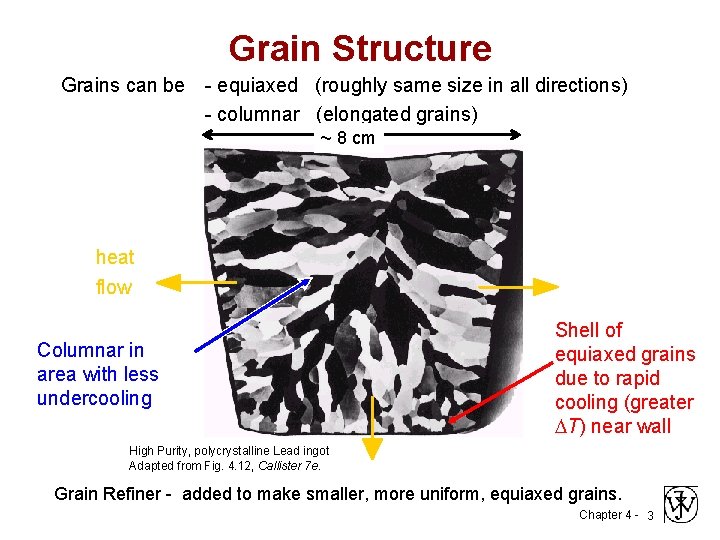
Grain Structure Grains can be - equiaxed (roughly same size in all directions) - columnar (elongated grains) ~ 8 cm heat flow Columnar in area with less undercooling Shell of equiaxed grains due to rapid cooling (greater T) near wall High Purity, polycrystalline Lead ingot Adapted from Fig. 4. 12, Callister 7 e. Grain Refiner - added to make smaller, more uniform, equiaxed grains. Chapter 4 - 3

Imperfections in Solids There is no such thing as a perfect crystal. • What are these imperfections? • Why are they important? Many of the important properties of materials are due to the presence of imperfections. Chapter 4 - 4

An ideal crystal can be described in terms a three-dimensionally periodic arrangement of points called lattice and an atom or group of atoms associated with each lattice point called unit cell: Crystal = Lattice + Unit Cell However, there can be deviations from this ideality. These deviations are known as crystal defects. Chapter 4 - 5

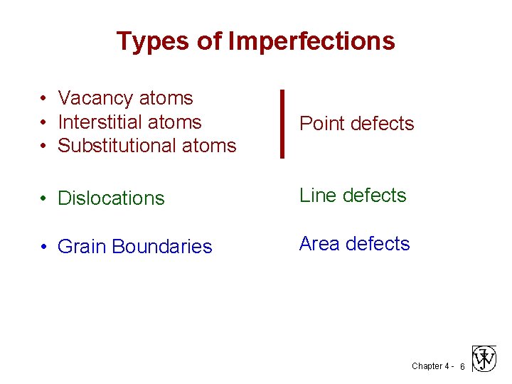
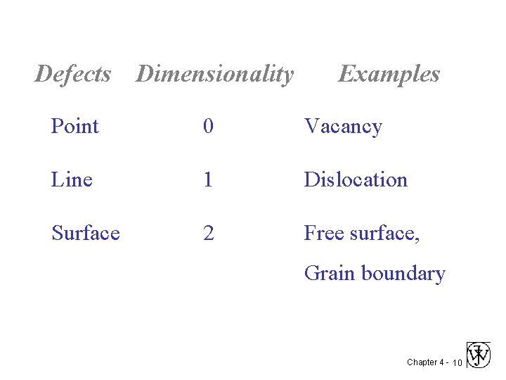
Types of Imperfections • Vacancy atoms • Interstitial atoms • Substitutional atoms Point defects • Dislocations Line defects • Grain Boundaries Area defects Chapter 4 - 6

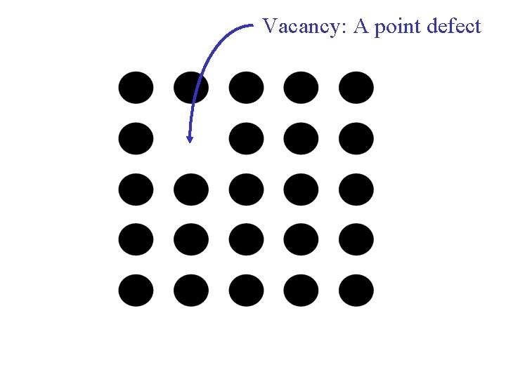
Vacancy: A point defect Chapter 4 - 7

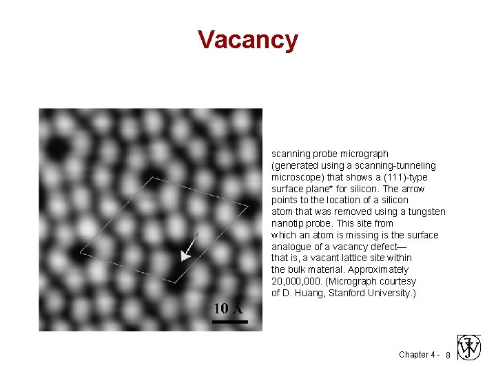
Vacancy scanning probe micrograph (generated using a scanning-tunneling microscope) that shows a (111)-type surface plane* for silicon. The arrow points to the location of a silicon atom that was removed using a tungsten nanotip probe. This site from which an atom is missing is the surface analogue of a vacancy defect— that is, a vacant lattice site within the bulk material. Approximately 20, 000. (Micrograph courtesy of D. Huang, Stanford University. ) Chapter 4 - 8

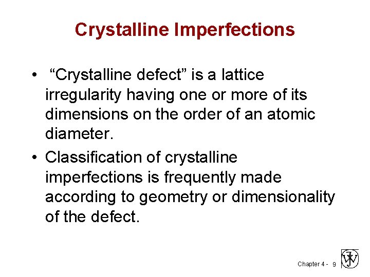
Crystalline Imperfections • “Crystalline defect” is a lattice irregularity having one or more of its dimensions on the order of an atomic diameter. • Classification of crystalline imperfections is frequently made according to geometry or dimensionality of the defect. Chapter 4 - 9

Defects Dimensionality Examples Point 0 Vacancy Line 1 Dislocation Surface 2 Free surface, Grain boundary Chapter 4 - 10

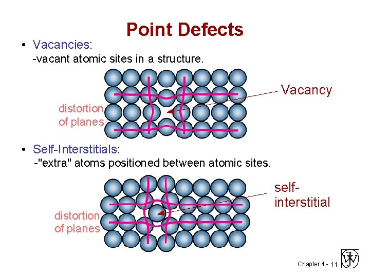
• Vacancies: Point Defects -vacant atomic sites in a structure. Vacancy distortion of planes • Self-Interstitials: -"extra" atoms positioned between atomic sites. distortion of planes selfinterstitial Chapter 4 - 11

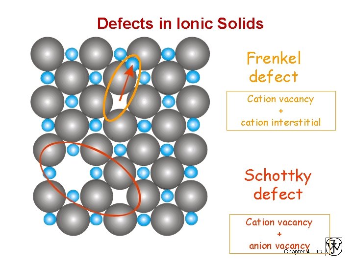
Defects in Ionic Solids Frenkel defect Cation vacancy + cation interstitial Schottky defect Cation vacancy + anion vacancy Chapter 4 - 12

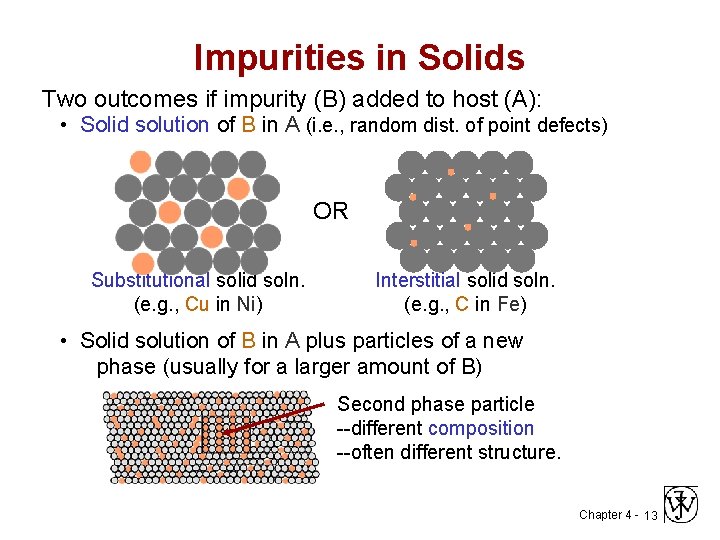
Impurities in Solids Two outcomes if impurity (B) added to host (A): • Solid solution of B in A (i. e. , random dist. of point defects) OR Substitutional solid soln. (e. g. , Cu in Ni) Interstitial solid soln. (e. g. , C in Fe) • Solid solution of B in A plus particles of a new phase (usually for a larger amount of B) Second phase particle --different composition --often different structure. Chapter 4 - 13

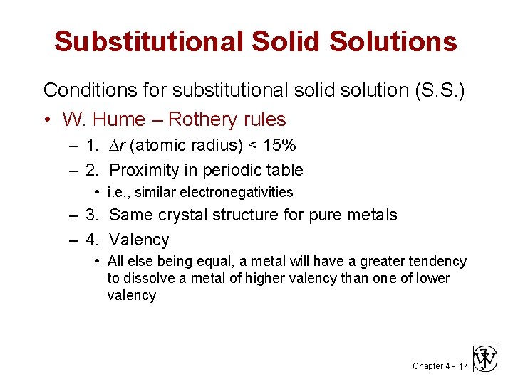
Substitutional Solid Solutions Conditions for substitutional solid solution (S. S. ) • W. Hume – Rothery rules – 1. r (atomic radius) < 15% – 2. Proximity in periodic table • i. e. , similar electronegativities – 3. Same crystal structure for pure metals – 4. Valency • All else being equal, a metal will have a greater tendency to dissolve a metal of higher valency than one of lower valency Chapter 4 - 14

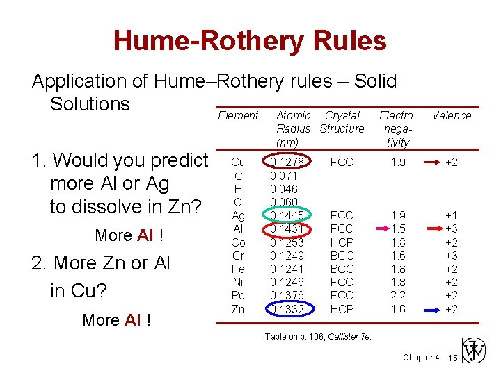
Hume-Rothery Rules Application of Hume–Rothery rules – Solid Solutions Element Atomic Crystal Electro. Radius Structure (nm) 1. Would you predict more Al or Ag to dissolve in Zn? More Al ! 2. More Zn or Al in Cu? More Al ! Cu C H O Ag Al Co Cr Fe Ni Pd Zn 0. 1278 0. 071 0. 046 0. 060 0. 1445 0. 1431 0. 1253 0. 1249 0. 1241 0. 1246 0. 1376 0. 1332 Valence negativity FCC 1. 9 +2 FCC HCP BCC FCC HCP 1. 9 1. 5 1. 8 1. 6 1. 8 2. 2 1. 6 +1 +3 +2 +2 Table on p. 106, Callister 7 e. Chapter 4 - 15

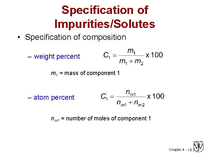
Specification of Impurities/Solutes • Specification of composition – weight percent m 1 = mass of component 1 – atom percent nm 1 = number of moles of component 1 Chapter 4 - 16

Line Defects Dislocations Chapter 4 - 17

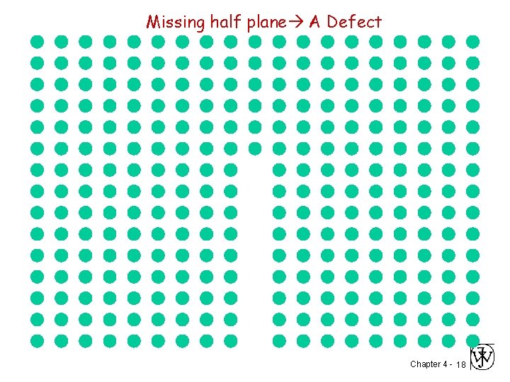
Missing half plane A Defect Chapter 4 - 18

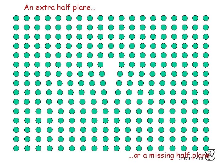
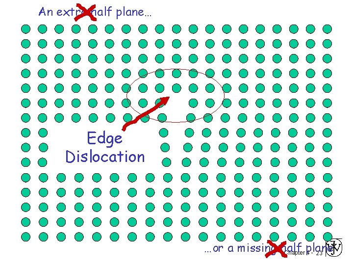
An extra half plane… …or a missing half Chapter plane 4 - 19

What kind of defect is this? A line defect? Or a planar defect? Chapter 4 - 20

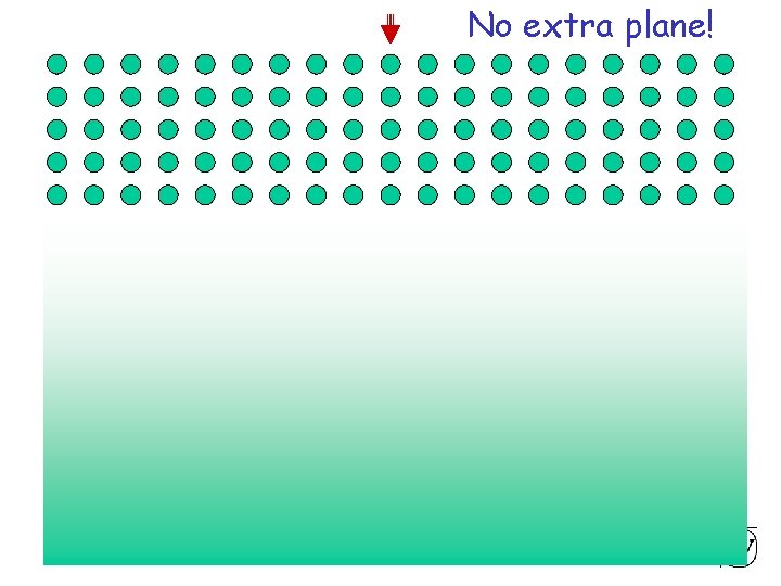
Extra half plane No extra plane! Chapter 4 - 21

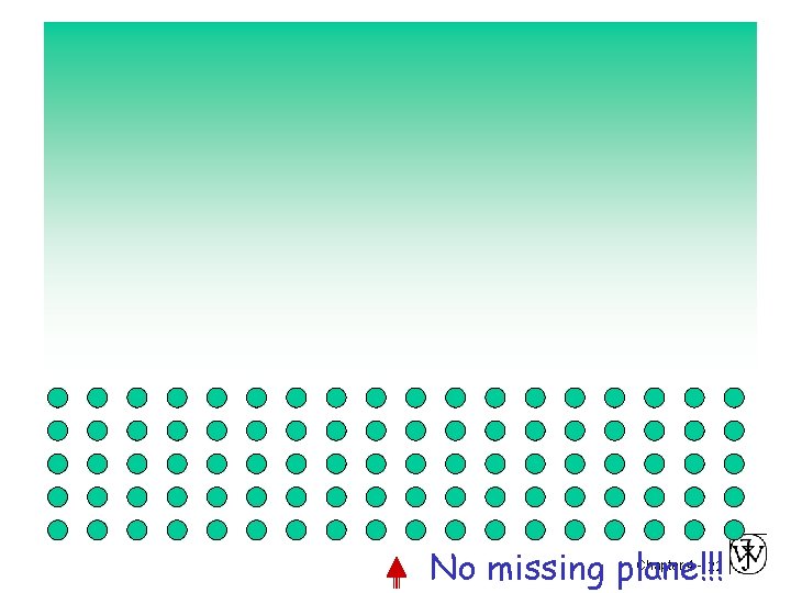
Missing plane No missing plane!!! Chapter 4 - 22

An extra half plane… Edge Dislocation …or a missing half Chapter plane 4 - 23

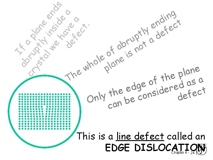
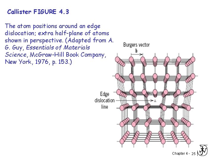
I ab f a cr ru p ys pt lan ta ly e l w in en e sid ds ha e de ve a fe a ct. g n i d t n c e e ly ef t p ad u r t b a o n f is o e e l n o h pla w e n a l e p h e h t T a f s o a d ge e d r e e t e d i c h s e t n f y o e l c d n e O b n a c This is a line defect called an EDGE DISLOCATION Chapter 4 - 24

Callister FIGURE 4. 3 The atom positions around an edge dislocation; extra half-plane of atoms shown in perspective. (Adapted from A. G. Guy, Essentials of Materials Science, Mc. Graw-Hill Book Company, New York, 1976, p. 153. ) Chapter 4 - 25

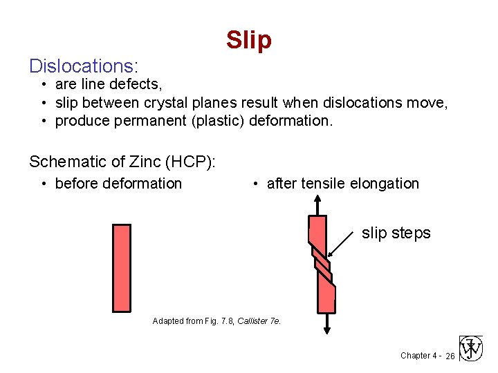
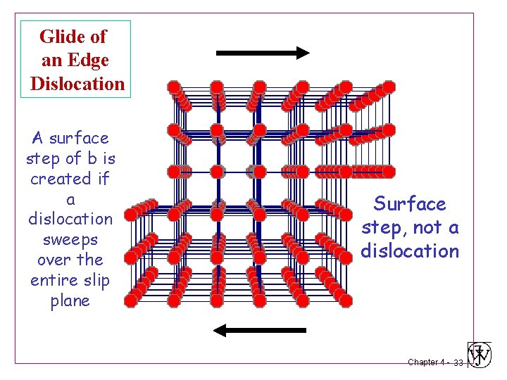
Slip Dislocations: • are line defects, • slip between crystal planes result when dislocations move, • produce permanent (plastic) deformation. Schematic of Zinc (HCP): • before deformation • after tensile elongation slip steps Adapted from Fig. 7. 8, Callister 7 e. Chapter 4 - 26

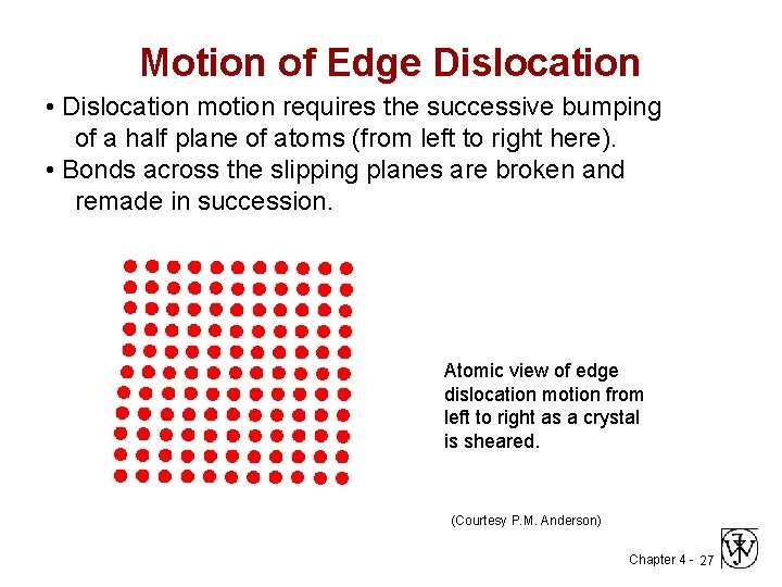
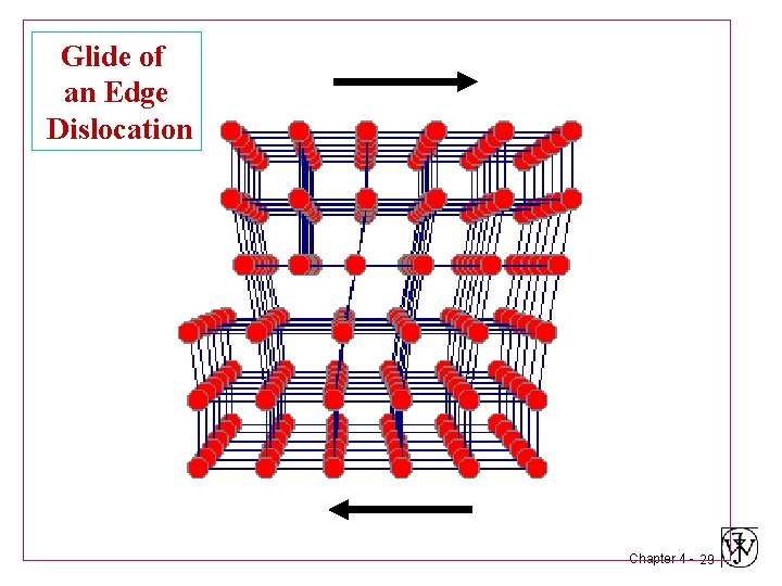
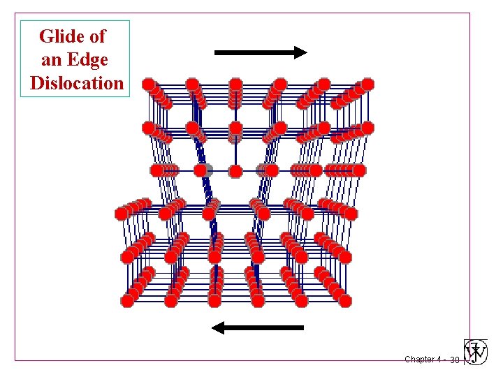
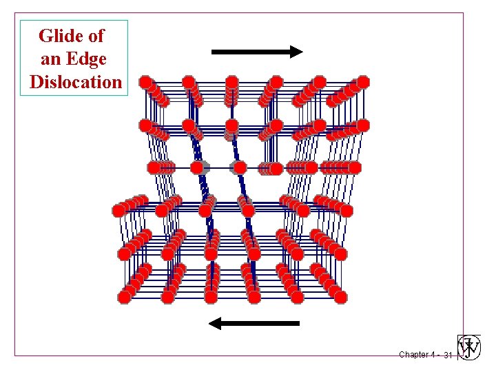
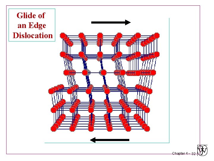
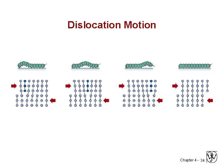
Motion of Edge Dislocation • Dislocation motion requires the successive bumping of a half plane of atoms (from left to right here). • Bonds across the slipping planes are broken and remade in succession. Atomic view of edge dislocation motion from left to right as a crystal is sheared. (Courtesy P. M. Anderson) Chapter 4 - 27

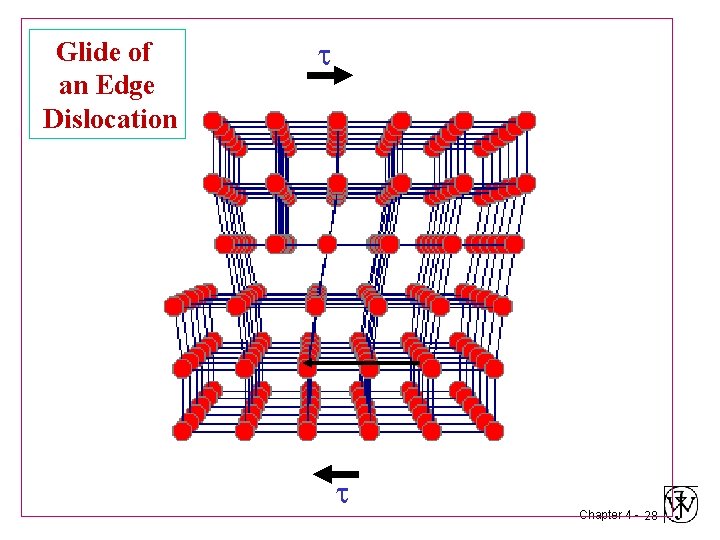
Glide of an Edge Dislocation Chapter 4 - 28

Glide of an Edge Dislocation Chapter 4 - 29

Glide of an Edge Dislocation Chapter 4 - 30

Glide of an Edge Dislocation Chapter 4 - 31

Glide of an Edge Dislocation Chapter 4 - 32

Glide of an Edge Dislocation A surface step of b is created if a dislocation sweeps over the entire slip plane Surface step, not a dislocation Chapter 4 - 33

Dislocation Motion Chapter 4 - 34

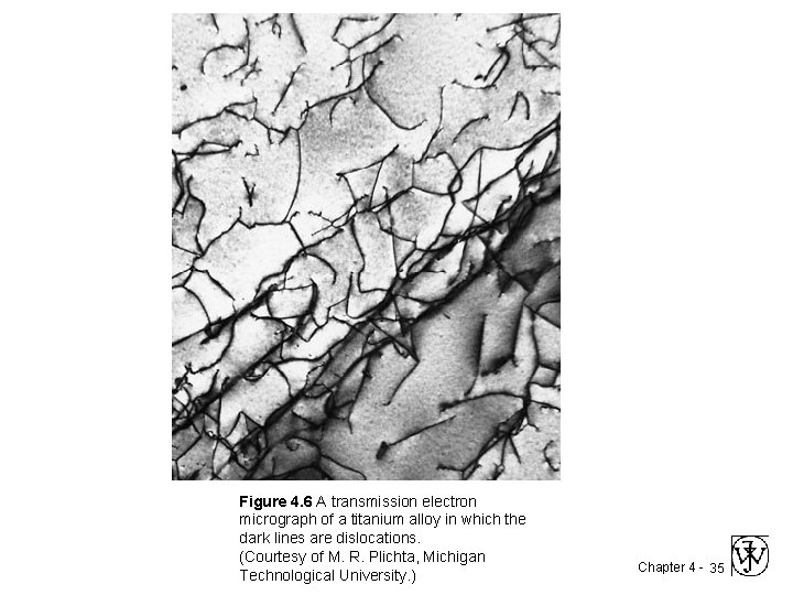
Figure 4. 6 A transmission electron micrograph of a titanium alloy in which the dark lines are dislocations. (Courtesy of M. R. Plichta, Michigan Technological University. ) Chapter 4 - 35

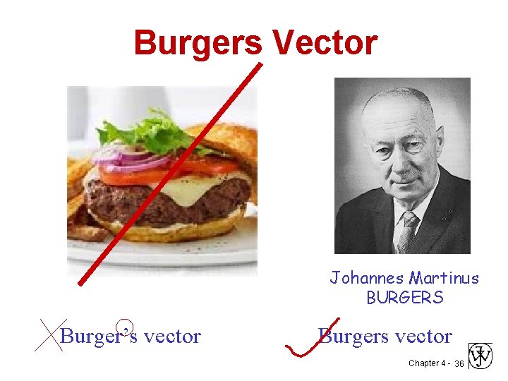
Burgers Vector Johannes Martinus BURGERS Burger’s vector Burgers vector Chapter 4 - 36

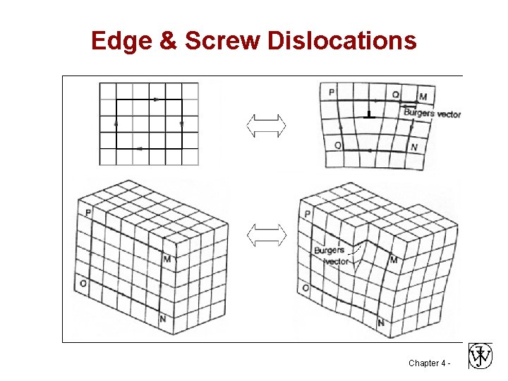
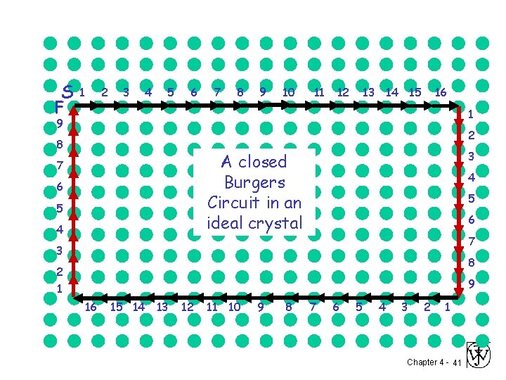
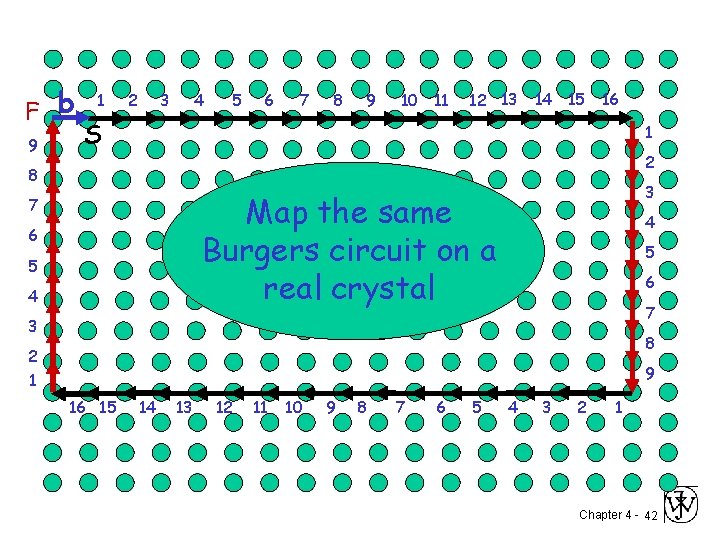
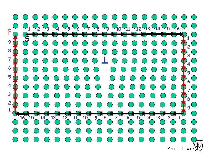
The magnitude and direction of the lattice distortion associated with a dislocation is expressed in terms of a Burgers vector, denoted by a b. For metallic materials, the Burgers vector for a dislocation will point in a close-packed crystallographic direction and will be of magnitude equal to the interatomic spacing. Chapter 4 - 37

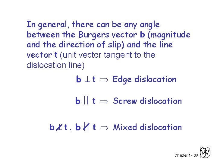
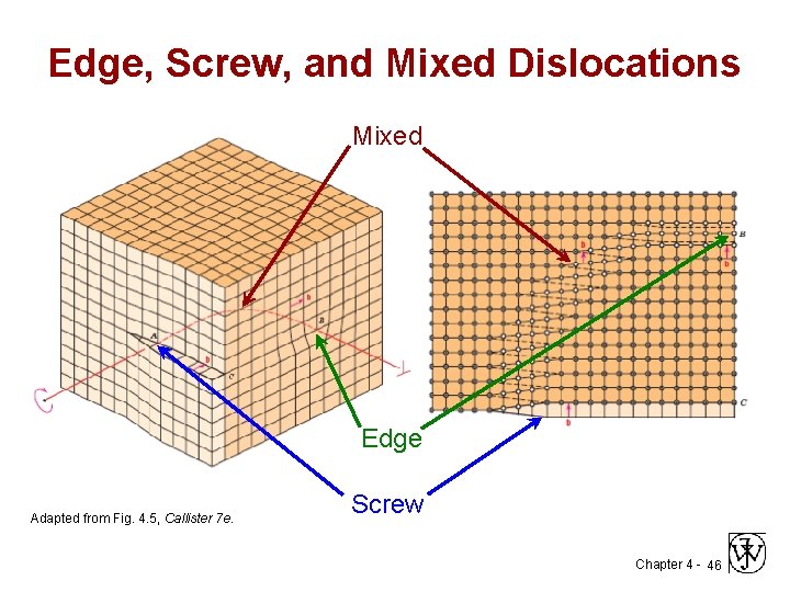
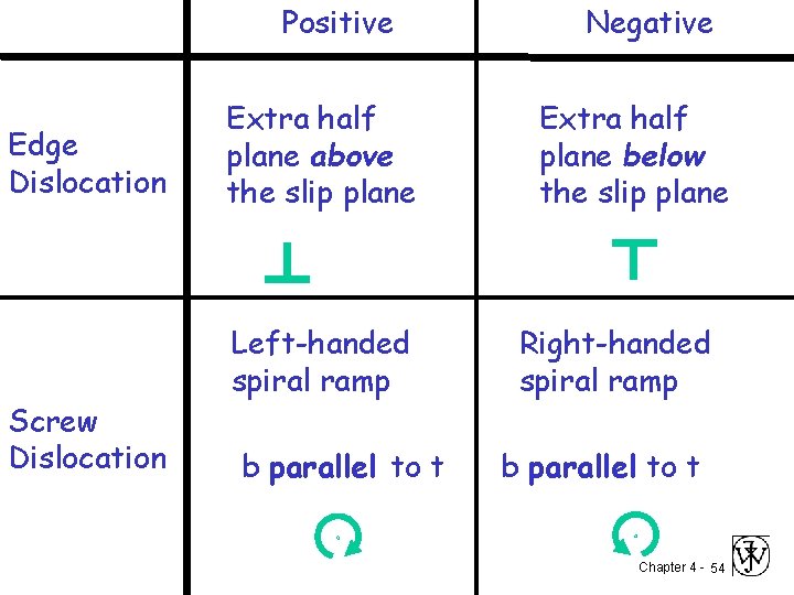
In general, there can be any angle between the Burgers vector b (magnitude and the direction of slip) and the line vector t (unit vector tangent to the dislocation line) b t Edge dislocation b t Screw dislocation b t , b t Mixed dislocation Chapter 4 - 38

Edge & Screw Dislocations Chapter 4 -

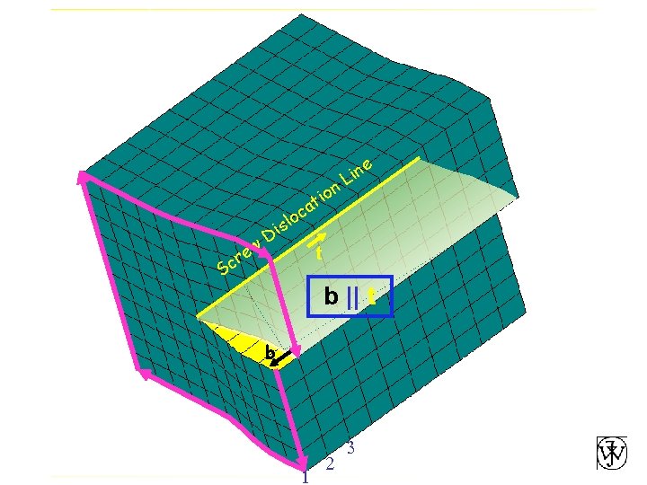
ion t ca e n i L o ew r c sl i D t S b || t b 1 2 3 Chapter 4 - 40

S F 1 2 3 4 5 6 7 8 9 10 11 12 13 14 15 16 1 9 2 8 3 A closed Burgers Circuit in an ideal crystal 7 6 5 4 4 5 6 7 3 8 2 1 9 16 15 14 13 12 11 10 9 8 7 6 5 4 3 2 1 Chapter 4 - 41

F b 9 1 2 3 4 5 6 7 8 9 10 11 12 13 14 15 16 S 1 2 8 3 same Map the Burgers circuit on a real crystal 7 6 5 4 4 5 6 7 3 8 2 1 9 16 15 14 13 12 11 10 9 8 7 6 5 4 3 2 1 Chapter 4 - 42

F 9 1 2 3 4 5 6 7 8 9 10 11 12 13 14 15 16 S 1 2 8 3 7 6 4 5 5 6 4 7 3 8 2 1 9 16 15 14 13 12 11 10 9 8 7 6 5 4 3 2 1 Chapter 4 - 43

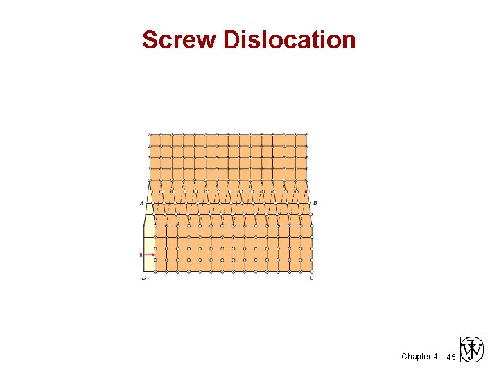
If b || t Then parallel planes to the dislocation line lose their distinct identity and become one continuous spiral ramp Hence the name SCREW DISLOCATION Chapter 4 - 44

Screw Dislocation Chapter 4 - 45

Edge, Screw, and Mixed Dislocations Mixed Edge Adapted from Fig. 4. 5, Callister 7 e. Screw Chapter 4 - 46

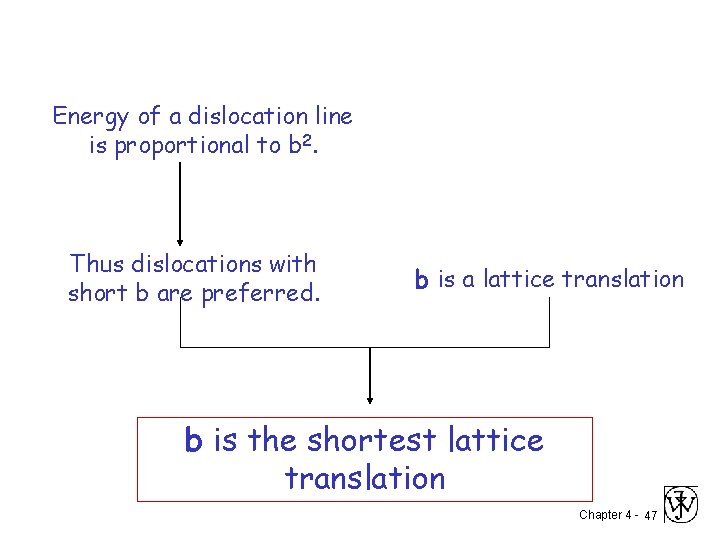
Energy of a dislocation line is proportional to b 2. Thus dislocations with short b are preferred. b is a lattice translation b is the shortest lattice translation Chapter 4 - 47

A dislocation line cannot end abruptly inside a crystal It can end on Free surfaces Grain boundaries On other dislocations at a point called a node On itself forming a loop Chapter 4 - 48

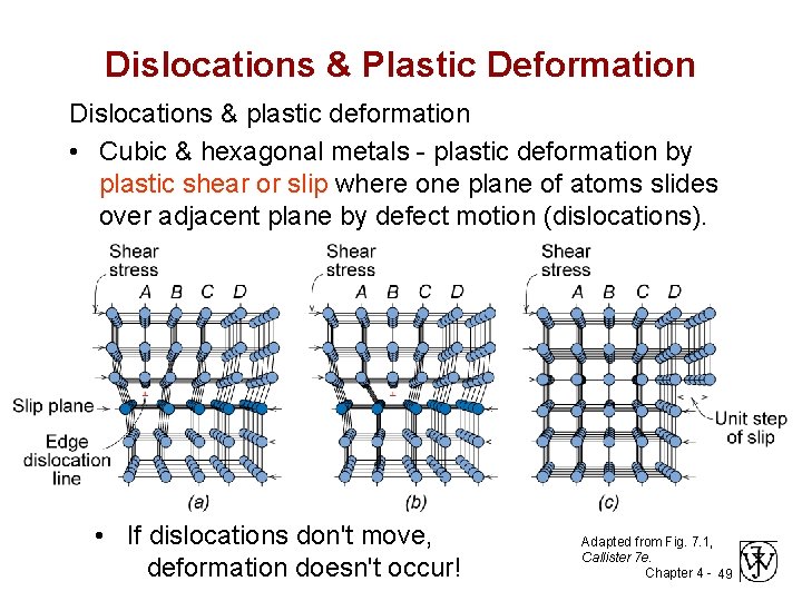
Dislocations & Plastic Deformation Dislocations & plastic deformation • Cubic & hexagonal metals - plastic deformation by plastic shear or slip where one plane of atoms slides over adjacent plane by defect motion (dislocations). • If dislocations don't move, deformation doesn't occur! Adapted from Fig. 7. 1, Callister 7 e. Chapter 4 - 49

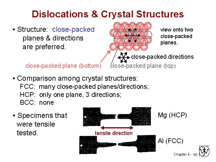
Dislocations & Crystal Structures • Structure: close-packed planes & directions are preferred. view onto two close-packed planes. close-packed plane (bottom) close-packed directions close-packed plane (top) • Comparison among crystal structures: FCC: many close-packed planes/directions; HCP: only one plane, 3 directions; BCC: none • Specimens that were tensile tested. Mg (HCP) tensile direction Al (FCC) Chapter 4 - 50

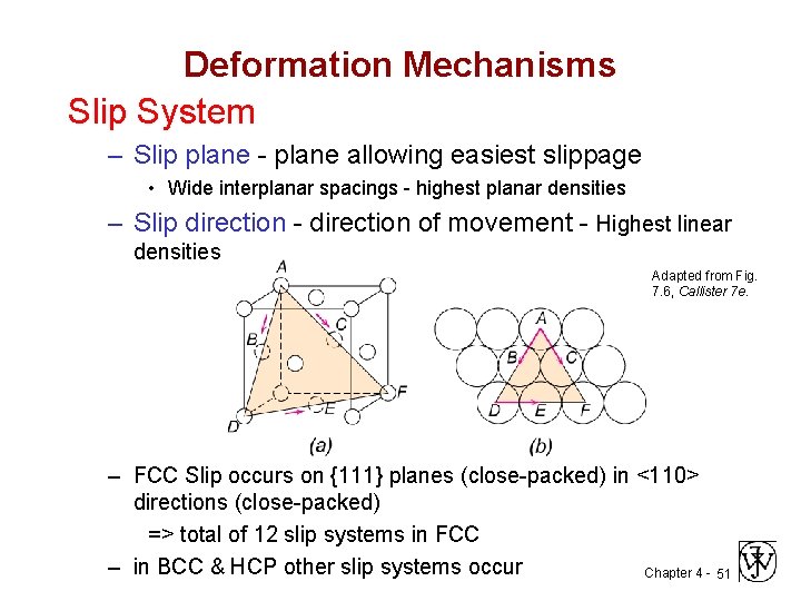
Deformation Mechanisms Slip System – Slip plane - plane allowing easiest slippage • Wide interplanar spacings - highest planar densities – Slip direction - direction of movement - Highest linear densities Adapted from Fig. 7. 6, Callister 7 e. – FCC Slip occurs on {111} planes (close-packed) in <110> directions (close-packed) => total of 12 slip systems in FCC – in BCC & HCP other slip systems occur Chapter 4 - 51

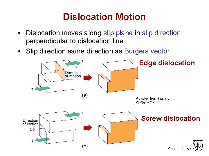
Dislocation Motion • Dislocation moves along slip plane in slip direction perpendicular to dislocation line • Slip direction same direction as Burgers vector Edge dislocation Adapted from Fig. 7. 2, Callister 7 e. Screw dislocation Chapter 4 - 52

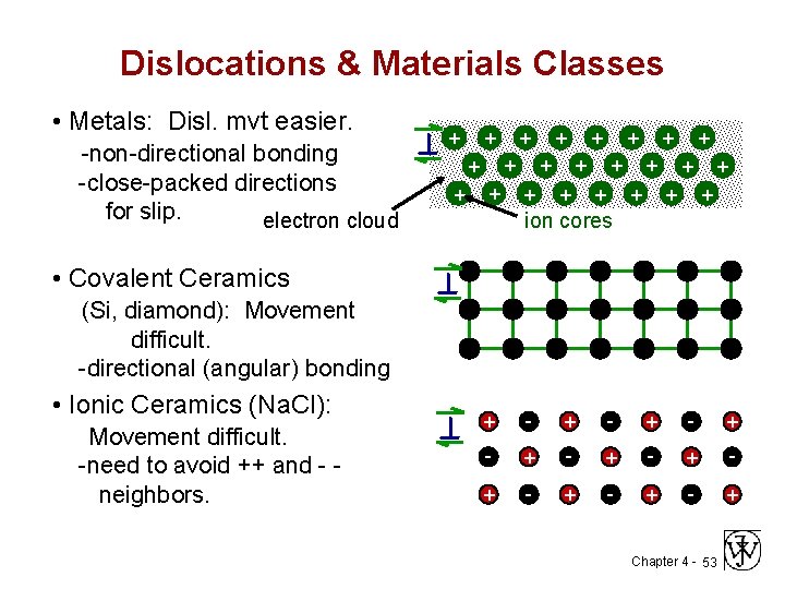
Dislocations & Materials Classes • Metals: Disl. mvt easier. -non-directional bonding -close-packed directions for slip. electron cloud + + + + + + ion cores • Covalent Ceramics (Si, diamond): Movement difficult. -directional (angular) bonding • Ionic Ceramics (Na. Cl): Movement difficult. -need to avoid ++ and - neighbors. + - + - + - + Chapter 4 - 53

Positive Edge Dislocation Screw Dislocation Extra half plane above the slip plane Left-handed spiral ramp b parallel to t Negative Extra half plane below the slip plane Right-handed spiral ramp b parallel to t Chapter 4 - 54

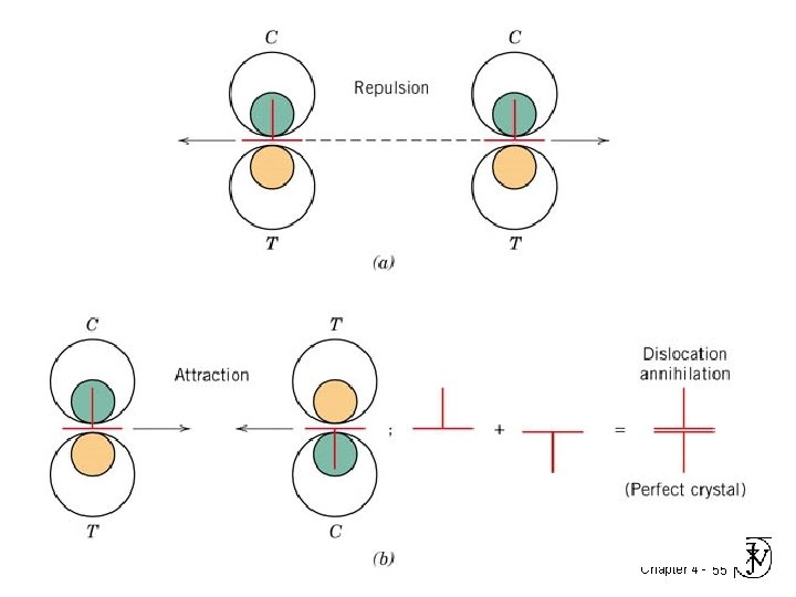
Chapter 4 - 55

Surface Defects Chapter 4 - 56

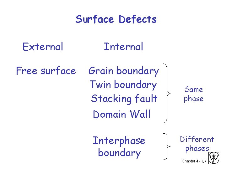
Surface Defects External Free surface Internal Grain boundary Twin boundary Stacking fault Same phase Domain Wall Interphase boundary Different phases Chapter 4 - 57

Surface energy is anisotropic Surface energy depends on the orientation, i. e. , the Miller indices of the free surface n. A, n. B are different for different surfaces Chapter 4 - 58

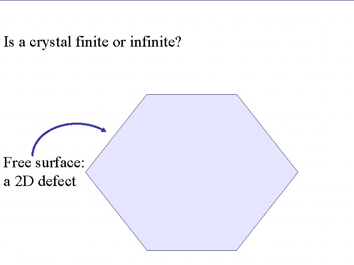
Is a lattice finite or infinite? Is a crystal finite or infinite? Free surface: a 2 D defect Chapter 4 - 59

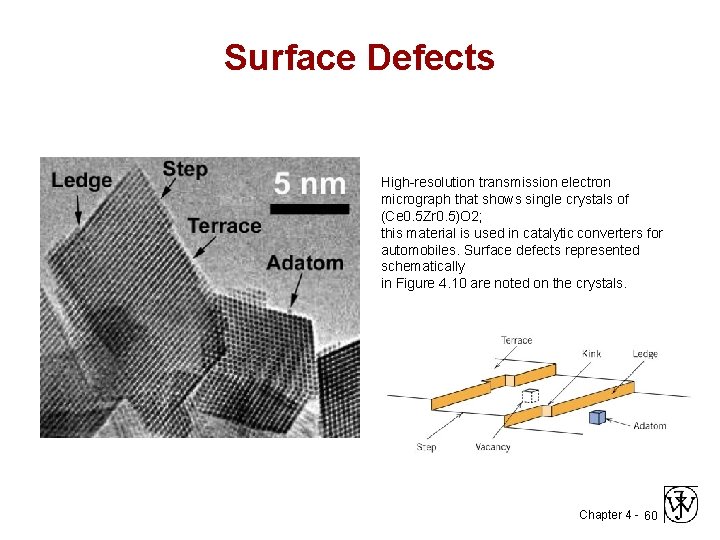
Surface Defects High-resolution transmission electron micrograph that shows single crystals of (Ce 0. 5 Zr 0. 5)O 2; this material is used in catalytic converters for automobiles. Surface defects represented schematically in Figure 4. 10 are noted on the crystals. Chapter 4 - 60

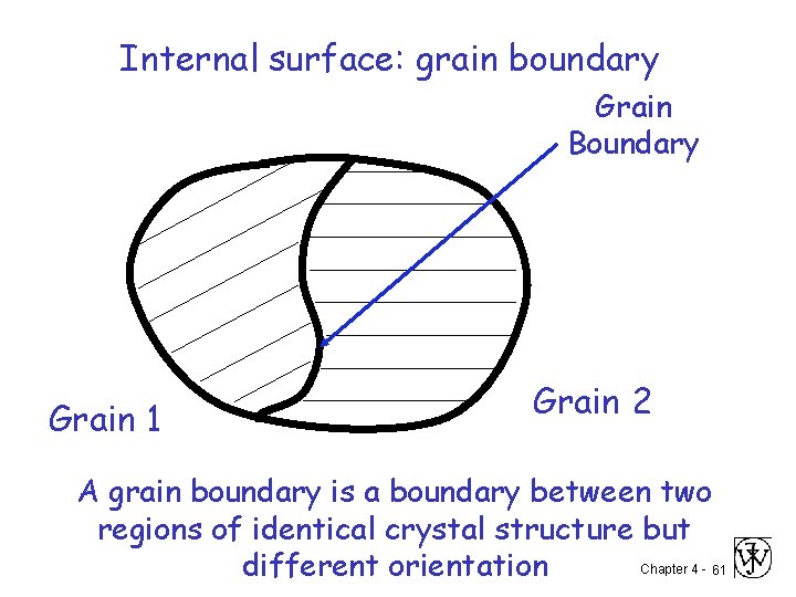
Internal surface: grain boundary Grain Boundary Grain 1 Grain 2 A grain boundary is a boundary between two regions of identical crystal structure but Chapter 4 - 61 different orientation

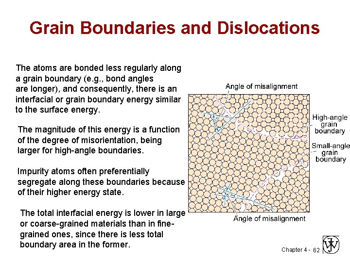
Grain Boundaries and Dislocations The atoms are bonded less regularly along a grain boundary (e. g. , bond angles are longer), and consequently, there is an interfacial or grain boundary energy similar to the surface energy. The magnitude of this energy is a function of the degree of misorientation, being larger for high-angle boundaries. Impurity atoms often preferentially segregate along these boundaries because of their higher energy state. The total interfacial energy is lower in large or coarse-grained materials than in finegrained ones, since there is less total boundary area in the former. Chapter 4 - 62

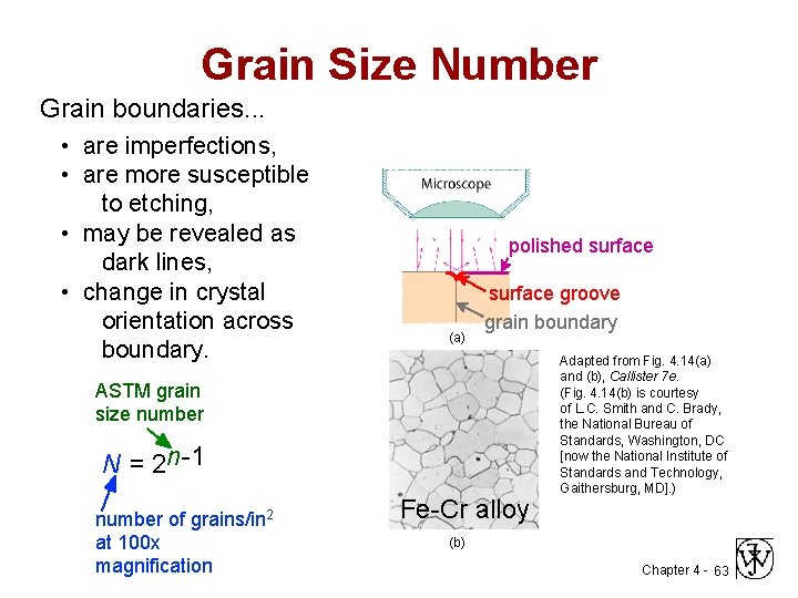
Grain Size Number Grain boundaries. . . • are imperfections, • are more susceptible to etching, • may be revealed as dark lines, • change in crystal orientation across boundary. polished surface (a) surface groove grain boundary ASTM grain size number N = 2 n-1 number of grains/in 2 at 100 x magnification Fe-Cr alloy Adapted from Fig. 4. 14(a) and (b), Callister 7 e. (Fig. 4. 14(b) is courtesy of L. C. Smith and C. Brady, the National Bureau of Standards, Washington, DC [now the National Institute of Standards and Technology, Gaithersburg, MD]. ) (b) Chapter 4 - 63

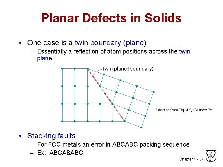
Planar Defects in Solids • One case is a twin boundary (plane) – Essentially a reflection of atom positions across the twin plane. Adapted from Fig. 4. 9, Callister 7 e. • Stacking faults – For FCC metals an error in ABCABC packing sequence – Ex: ABCABABC Chapter 4 - 64

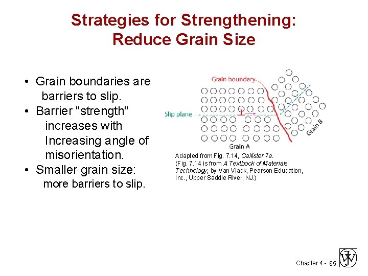
Strategies for Strengthening: Reduce Grain Size • Grain boundaries are barriers to slip. • Barrier "strength" increases with Increasing angle of misorientation. • Smaller grain size: more barriers to slip. Adapted from Fig. 7. 14, Callister 7 e. (Fig. 7. 14 is from A Textbook of Materials Technology, by Van Vlack, Pearson Education, Inc. , Upper Saddle River, NJ. ) Chapter 4 - 65

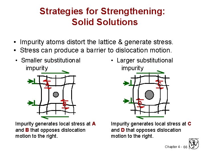
Strategies for Strengthening: Solid Solutions • Impurity atoms distort the lattice & generate stress. • Stress can produce a barrier to dislocation motion. • Smaller substitutional impurity • Larger substitutional impurity A C B Impurity generates local stress at A and B that opposes dislocation motion to the right. D Impurity generates local stress at C and D that opposes dislocation motion to the right. Chapter 4 - 66

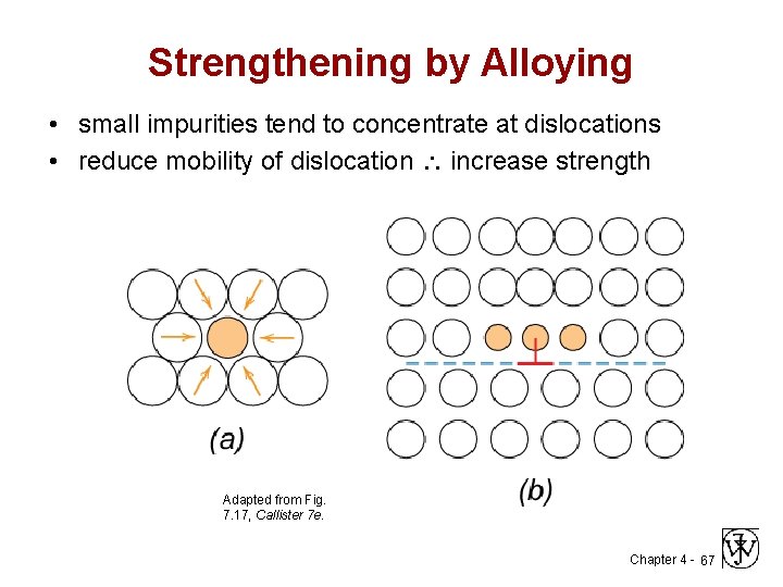
Strengthening by Alloying • small impurities tend to concentrate at dislocations • reduce mobility of dislocation increase strength Adapted from Fig. 7. 17, Callister 7 e. Chapter 4 - 67

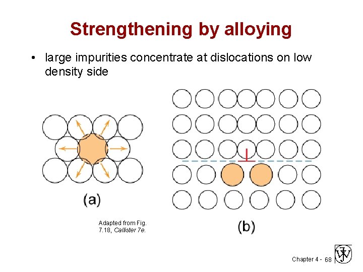
Strengthening by alloying • large impurities concentrate at dislocations on low density side Adapted from Fig. 7. 18, Callister 7 e. Chapter 4 - 68

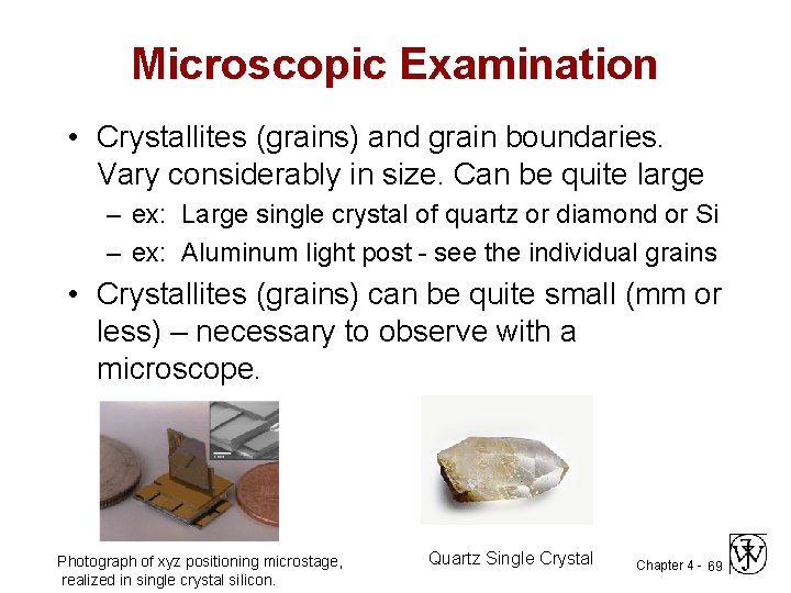
Microscopic Examination • Crystallites (grains) and grain boundaries. Vary considerably in size. Can be quite large – ex: Large single crystal of quartz or diamond or Si – ex: Aluminum light post - see the individual grains • Crystallites (grains) can be quite small (mm or less) – necessary to observe with a microscope. Photograph of xyz positioning microstage, realized in single crystal silicon. Quartz Single Crystal Chapter 4 - 69

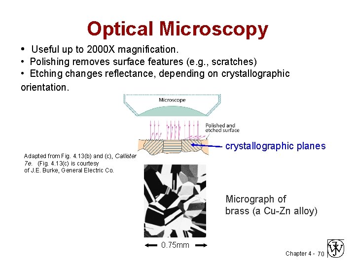
Optical Microscopy • Useful up to 2000 X magnification. • Polishing removes surface features (e. g. , scratches) • Etching changes reflectance, depending on crystallographic orientation. crystallographic planes Adapted from Fig. 4. 13(b) and (c), Callister 7 e. (Fig. 4. 13(c) is courtesy of J. E. Burke, General Electric Co. Micrograph of brass (a Cu-Zn alloy) 0. 75 mm Chapter 4 - 70

Polarized Light – metallographic scopes often use polarized light to increase contrast – Also used for transparent samples such as polymers Chapter 4 - 71

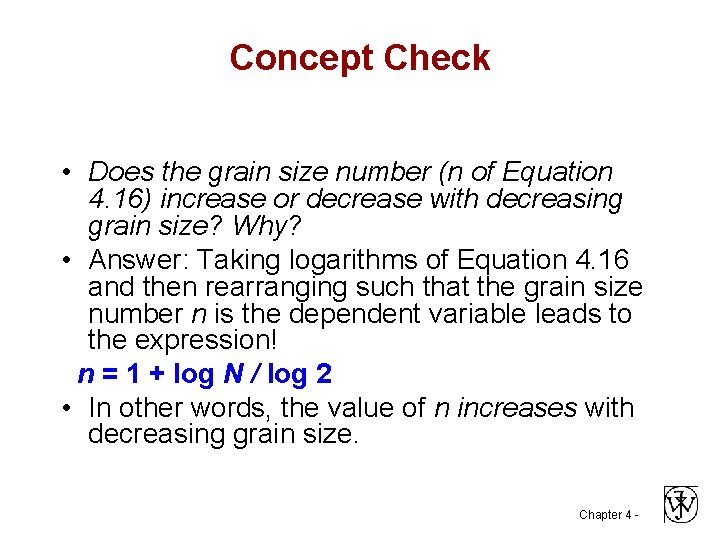
Concept Check • Does the grain size number (n of Equation 4. 16) increase or decrease with decreasing grain size? Why? • Answer: Taking logarithms of Equation 4. 16 and then rearranging such that the grain size number n is the dependent variable leads to the expression! n = 1 + log N / log 2 • In other words, the value of n increases with decreasing grain size. Chapter 4 -

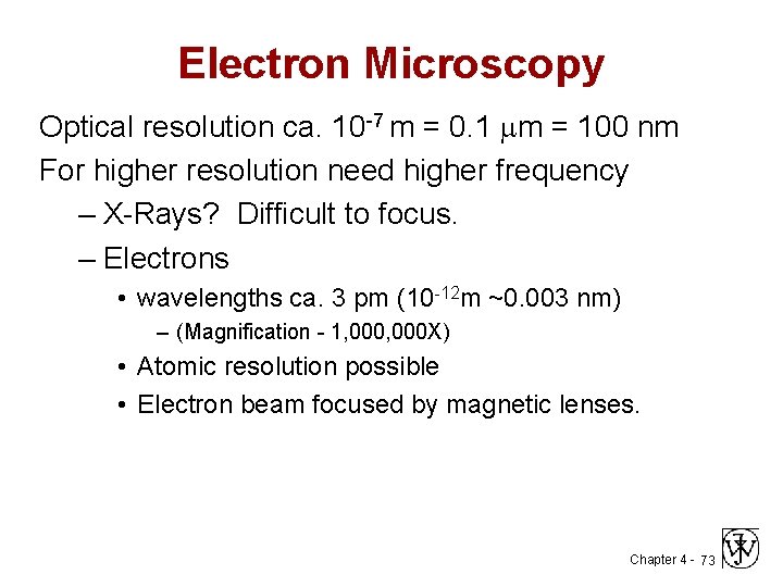
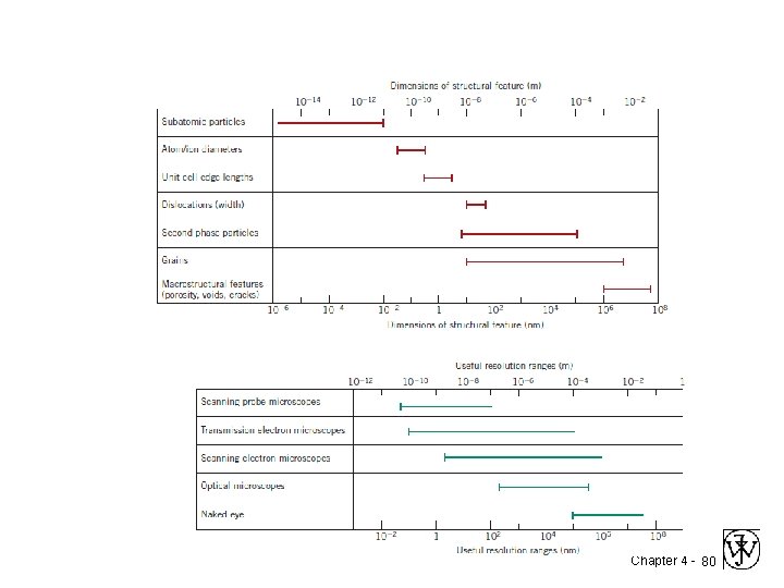
Electron Microscopy Optical resolution ca. 10 -7 m = 0. 1 m = 100 nm For higher resolution need higher frequency – X-Rays? Difficult to focus. – Electrons • wavelengths ca. 3 pm (10 -12 m ~0. 003 nm) – (Magnification - 1, 000 X) • Atomic resolution possible • Electron beam focused by magnetic lenses. Chapter 4 - 73

Scanning Probe Microscopy • Neither light nor electrons are used to form an image! • The microscope generates a topographical map, on an atomic scale, that is a representation of the surface features and characteristics of the specimen. • Examination on the nanometer scale is possible, magnifications as high as 109 x are possible; • Three-dimensional magnified images are generated that provide topographical information about features of interest. • Some SPMs may be operated in a variety of environments (e. g. , vacuum, air, liquid); thus, a particular specimen may be examined in its most suitable environment. Chapter 4 - 74

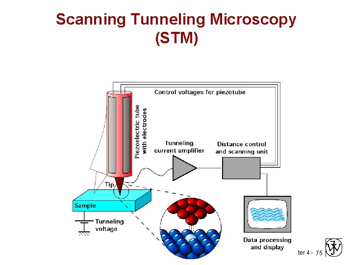
Scanning Tunneling Microscopy (STM) Chapter 4 - 75

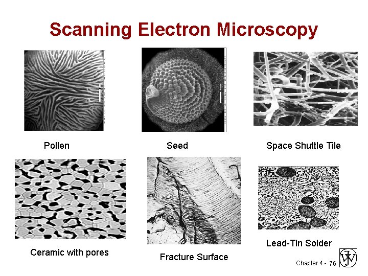
Scanning Electron Microscopy Pollen Ceramic with pores Seed Space Shuttle Tile Lead-Tin Solder Fracture Surface Chapter 4 - 76

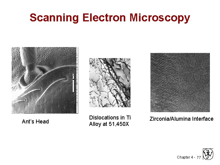
Scanning Electron Microscopy Ant’s Head Dislocations in Ti Alloy at 51, 450 X Zirconia/Alumina Interface Chapter 4 - 77

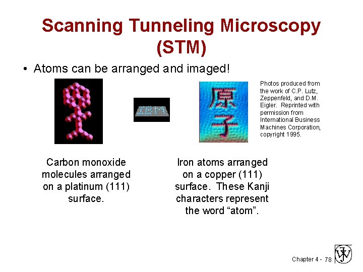
Scanning Tunneling Microscopy (STM) • Atoms can be arranged and imaged! Photos produced from the work of C. P. Lutz, Zeppenfeld, and D. M. Eigler. Reprinted with permission from International Business Machines Corporation, copyright 1995. Carbon monoxide molecules arranged on a platinum (111) surface. Iron atoms arranged on a copper (111) surface. These Kanji characters represent the word “atom”. Chapter 4 - 78

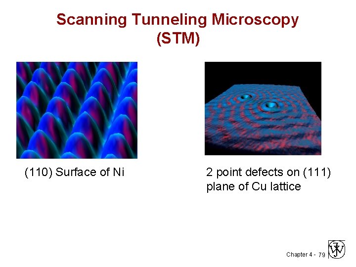
Scanning Tunneling Microscopy (STM) (110) Surface of Ni 2 point defects on (111) plane of Cu lattice Chapter 4 - 79

Chapter 4 - 80

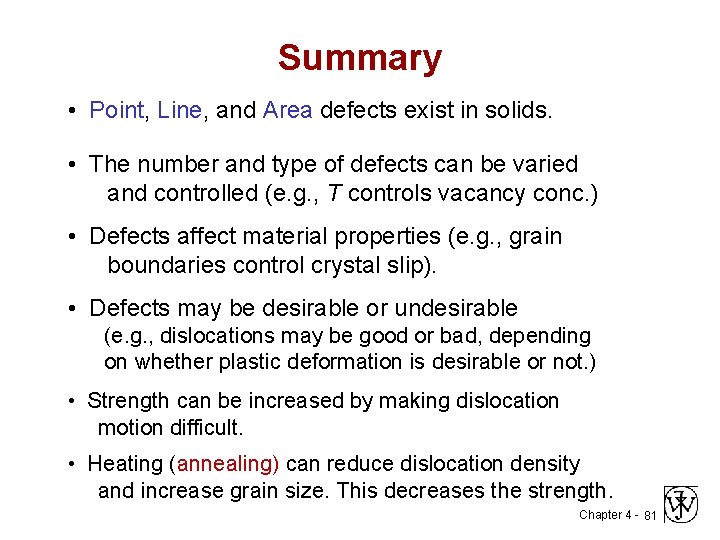
Summary • Point, Line, and Area defects exist in solids. • The number and type of defects can be varied and controlled (e. g. , T controls vacancy conc. ) • Defects affect material properties (e. g. , grain boundaries control crystal slip). • Defects may be desirable or undesirable (e. g. , dislocations may be good or bad, depending on whether plastic deformation is desirable or not. ) • Strength can be increased by making dislocation motion difficult. • Heating (annealing) can reduce dislocation density and increase grain size. This decreases the strength. Chapter 4 - 81