Chapter 5 Imperfections in Solids ISSUES TO ADDRESS

- Slides: 44

Chapter 5: Imperfections in Solids ISSUES TO ADDRESS. . . • What types of defects exist in solid materials? • How does the number of vacancies depend on temperature? • What are the two types of solid solutions? • What are three types of dislocations? • What kinds of information come from microscopic examinations? Chapter 5 - 1

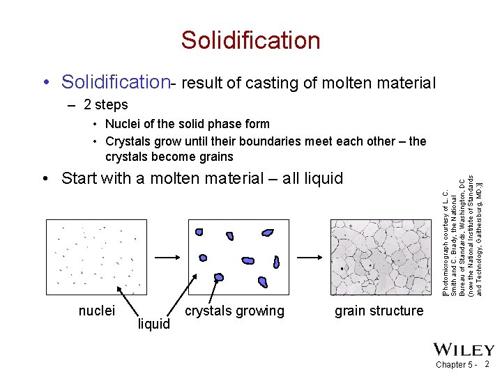
Solidification • Solidification- result of casting of molten material – 2 steps • Start with a molten material – all liquid nuclei liquid crystals growing [Photomicrograph courtesy of L. C. Smith and C. Brady, the National Bureau of Standards, Washington, DC (now the National Institute of Standards and Technology, Gaithersburg, MD. )] • Nuclei of the solid phase form • Crystals grow until their boundaries meet each other – the crystals become grains grain structure Chapter 5 - 2

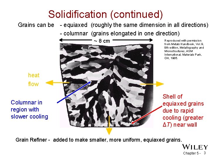
Solidification (continued) Grains can be - equiaxed (roughly the same dimension in all directions) - columnar (grains elongated in one direction) ~ 8 cm Reproduced with permission from Metals Handbook, Vol. 9, 9 th edition, Metallography and Microstructures, ASM International, Materials Park, OH, 1985. heat flow Columnar in region with slower cooling Shell of equiaxed grains due to rapid cooling (greater ΔT) near wall Grain Refiner - added to make smaller, more uniform, equiaxed grains. Chapter 5 - 3

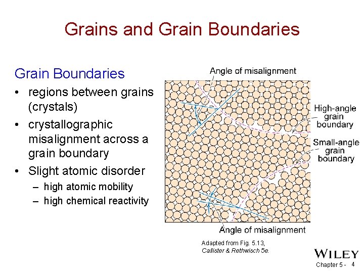
Grains and Grain Boundaries • regions between grains (crystals) • crystallographic misalignment across a grain boundary • Slight atomic disorder – high atomic mobility – high chemical reactivity Adapted from Fig. 5. 13, Callister & Rethwisch 5 e. Chapter 5 - 4

Imperfections in Solids There is no such thing as a perfect crystal. Crystalline imperfections (or defects) are always present. • Many of the properties of materials are sensitive to the presence of imperfections. • Crystalline defect refers to a lattice irregularity with dimensions on the order of an atomic diameter. • What kinds of crystalline imperfections exist in solids? Chapter 5 - 5

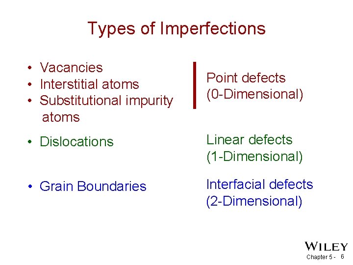
Types of Imperfections • Vacancies • Interstitial atoms • Substitutional impurity atoms Point defects (0 -Dimensional) • Dislocations Linear defects (1 -Dimensional) • Grain Boundaries Interfacial defects (2 -Dimensional) Chapter 5 - 6

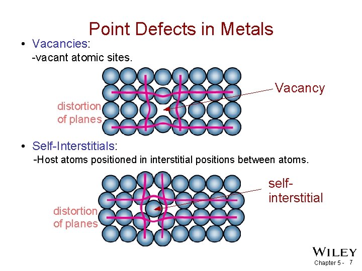
Point Defects in Metals • Vacancies: -vacant atomic sites. Vacancy distortion of planes • Self-Interstitials: -Host atoms positioned in interstitial positions between atoms. distortion of planes selfinterstitial Chapter 5 - 7

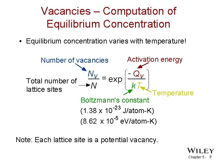
Vacancies – Computation of Equilibrium Concentration • Equilibrium concentration varies with temperature! Number of vacancies Total number of lattice sites Activation energy - Qv Nv = exp N k. T Temperature Boltzmann's constant -23 (1. 38 x 10 J/atom-K) -5 (8. 62 x 10 e. V/atom-K) Note: Each lattice site is a potential vacancy. Chapter 5 - 8

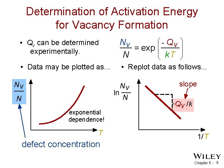
Determination of Activation Energy for Vacancy Formation • Qv can be determined experimentally. Nv - Qv = exp N k. T • Data may be plotted as. . . • Replot data as follows. . . Nv ln N exponential dependence! T defect concentration Nv N slope -Qv /k 1/T Chapter 5 - 9

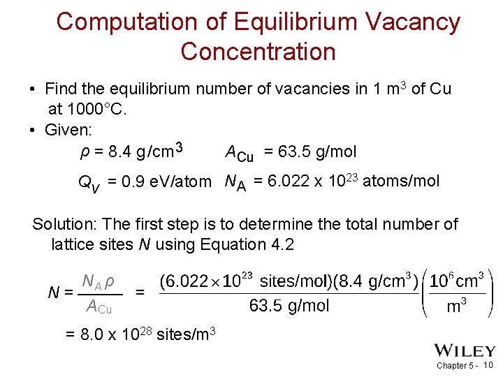
Computation of Equilibrium Vacancy Concentration • Find the equilibrium number of vacancies in 1 m 3 of Cu at 1000°C. • Given: ρ = 8. 4 g/cm 3 A Cu = 63. 5 g/mol Qv = 0. 9 e. V/atom NA = 6. 022 x 1023 atoms/mol Solution: The first step is to determine the total number of lattice sites N using Equation 4. 2 NA ρ N= A Cu = = 8. 0 x 1028 sites/m 3 Chapter 5 - 10

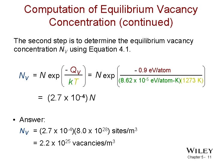
Computation of Equilibrium Vacancy Concentration (continued) The second step is to determine the equilibrium vacancy concentration NV using Equation 4. 1. - Qv = N exp Nv = N exp k. T - 0. 9 e. V/atom (8. 62 x 10 -5 e. V/atom-K)(1273 K) = (2. 7 x 10 -4) N • Answer: Nv = (2. 7 x 10 -4)(8. 0 x 1028) sites/m 3 = 2. 2 x 1025 vacancies/m 3 Chapter 5 - 11

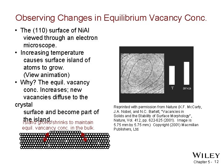
Observing Changes in Equilibrium Vacancy Conc. • The (110) surface of Ni. Al viewed through an electron microscope. • Increasing temperature causes surface island of atoms to grow. (View animation) • Why? The equil. vacancy conc. Increases; new vacancies diffuse to the crystal surface and become part of the island. Island grows/shrinks to maintain equil. vancancy conc. in the bulk. Reprinted with permission from Nature (K. F. Mc. Carty, J. A. Nobel, and N. C. Bartelt, "Vacancies in Solids and the Stability of Surface Morphology", Nature, Vol. 412, pp. 622 -625 (2001). Image is 5. 75 mm by 5. 75 mm. ) Copyright (2001) Macmillan Publishers, Ltd. Chapter 5 - 12

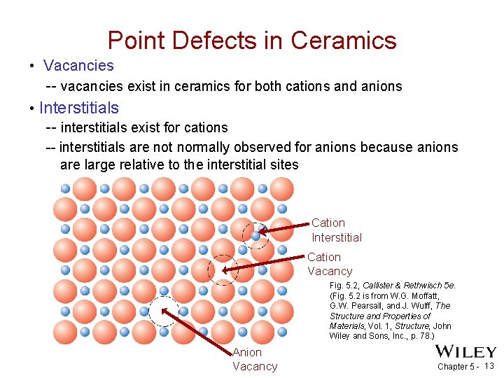
Point Defects in Ceramics • Vacancies -- vacancies exist in ceramics for both cations and anions • Interstitials -- interstitials exist for cations -- interstitials are not normally observed for anions because anions are large relative to the interstitial sites Cation Interstitial Cation Vacancy Fig. 5. 2, Callister & Rethwisch 5 e. (Fig. 5. 2 is from W. G. Moffatt, G. W. Pearsall, and J. Wulff, The Structure and Properties of Materials, Vol. 1, Structure, John Wiley and Sons, Inc. , p. 78. ) Anion Vacancy Chapter 5 - 13

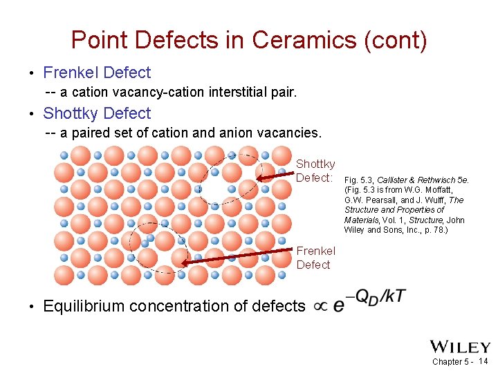
Point Defects in Ceramics (cont) • Frenkel Defect -- a cation vacancy-cation interstitial pair. • Shottky Defect -- a paired set of cation and anion vacancies. Shottky Defect: Fig. 5. 3, Callister & Rethwisch 5 e. (Fig. 5. 3 is from W. G. Moffatt, G. W. Pearsall, and J. Wulff, The Structure and Properties of Materials, Vol. 1, Structure, John Wiley and Sons, Inc. , p. 78. ) Frenkel Defect • Equilibrium concentration of defects Chapter 5 - 14

Chapter 5 - 15

Chapter 5 - 16

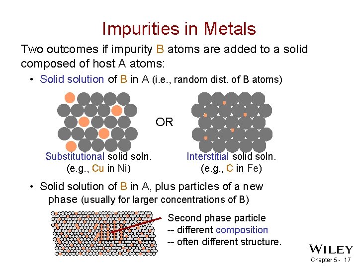
Impurities in Metals Two outcomes if impurity B atoms are added to a solid composed of host A atoms: • Solid solution of B in A (i. e. , random dist. of B atoms) OR Substitutional solid soln. (e. g. , Cu in Ni) Interstitial solid soln. (e. g. , C in Fe) • Solid solution of B in A, plus particles of a new phase (usually for larger concentrations of B) Second phase particle -- different composition -- often different structure. Chapter 5 - 17

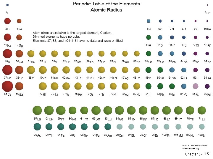
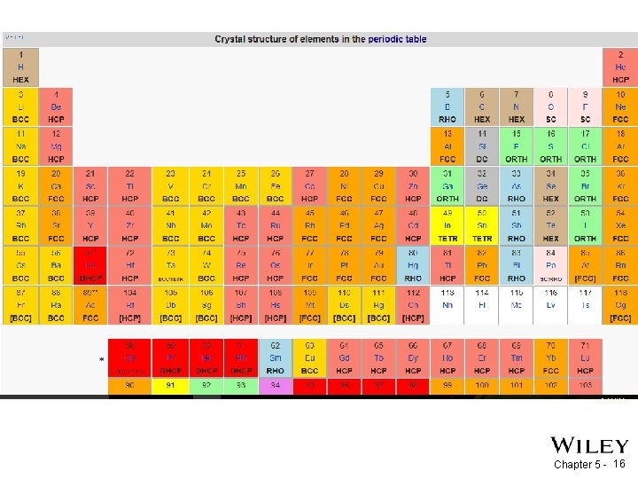
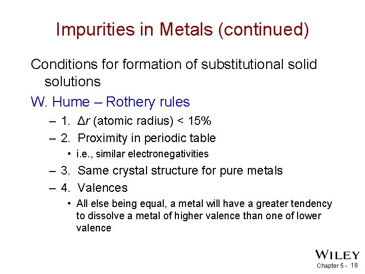
Impurities in Metals (continued) Conditions formation of substitutional solid solutions W. Hume – Rothery rules – 1. Δr (atomic radius) < 15% – 2. Proximity in periodic table • i. e. , similar electronegativities – 3. Same crystal structure for pure metals – 4. Valences • All else being equal, a metal will have a greater tendency to dissolve a metal of higher valence than one of lower valence Chapter 5 - 18

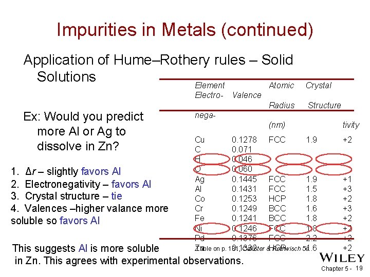
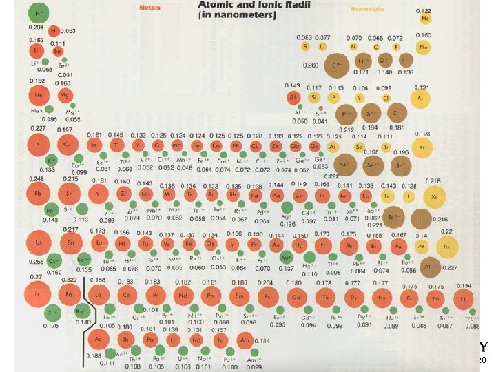
Impurities in Metals (continued) Application of Hume–Rothery rules – Solid Solutions Element Atomic Electro- Ex: Would you predict more Al or Ag to dissolve in Zn? 1. Δr – slightly favors Al 2. Electronegativity – favors Al 3. Crystal structure – tie 4. Valences –higher valance more soluble so favors Al Crystal Valence Radius Structure nega(nm) Cu 0. 1278 FCC 1. 9 C 0. 071 H 0. 046 O 0. 060 Ag 0. 1445 FCC 1. 9 Al 0. 1431 FCC 1. 5 Co 0. 1253 HCP 1. 8 Cr 0. 1249 BCC 1. 6 Fe 0. 1241 BCC 1. 8 Ni 0. 1246 FCC 1. 8 Pd 0. 1376 FCC 2. 2 Table on p. 181, Callister &HCP Rethwisch 5 e. Zn 0. 1332 1. 6 This suggests Al is more soluble in Zn. This agrees with experimental observations. tivity +2 +1 +3 +2 +2 Chapter 5 - 19

Chapter 5 - 20

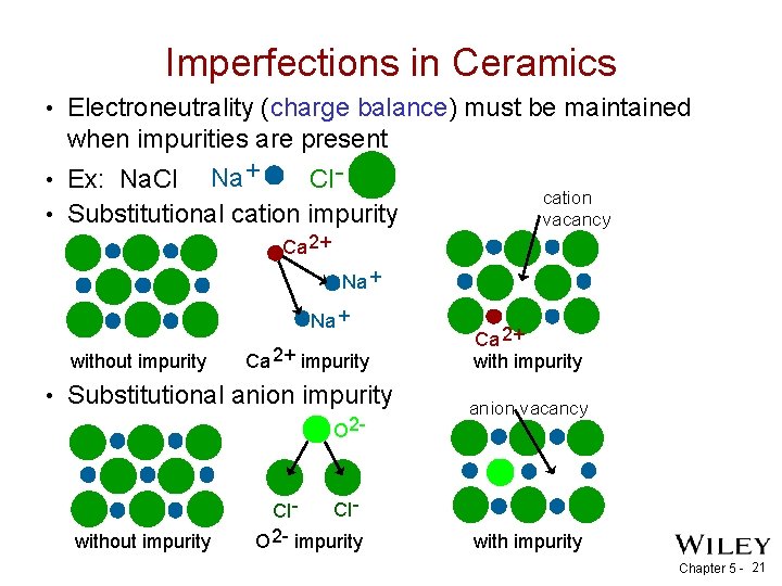
Imperfections in Ceramics • Electroneutrality (charge balance) must be maintained when impurities are present Cl • Ex: Na. Cl Na + • Substitutional cation impurity cation vacancy Ca 2+ Na + without impurity Ca 2+ impurity • Substitutional anion impurity O 2 - without impurity Cl Cl O 2 - impurity Ca 2+ with impurity anion vacancy with impurity Chapter 5 - 21

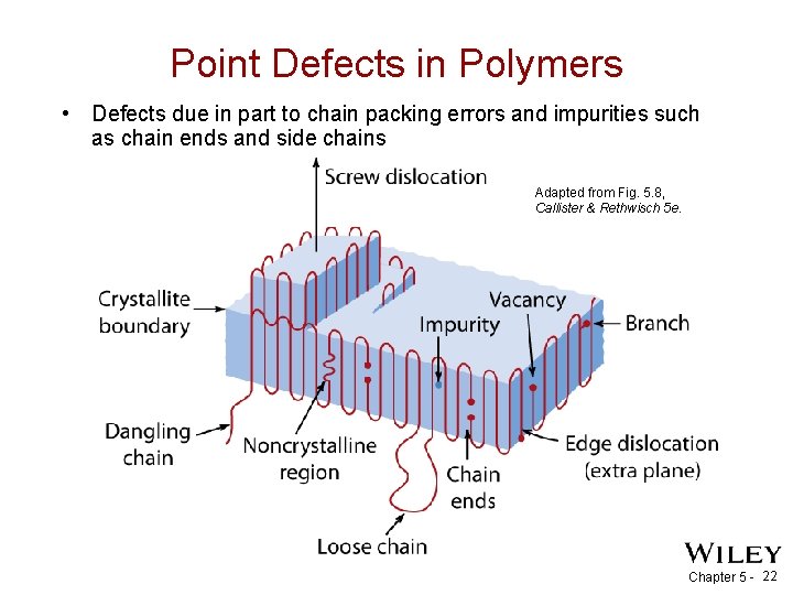
Point Defects in Polymers • Defects due in part to chain packing errors and impurities such as chain ends and side chains Adapted from Fig. 5. 8, Callister & Rethwisch 5 e. Chapter 5 - 22

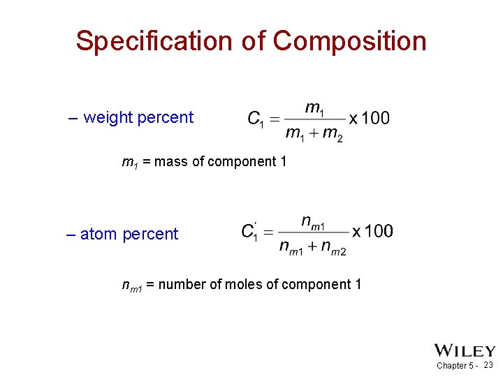
Specification of Composition – weight percent m 1 = mass of component 1 – atom percent nm 1 = number of moles of component 1 Chapter 5 - 23

Chapter 5 - 24

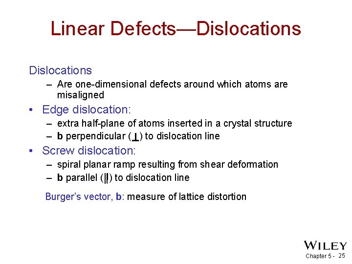
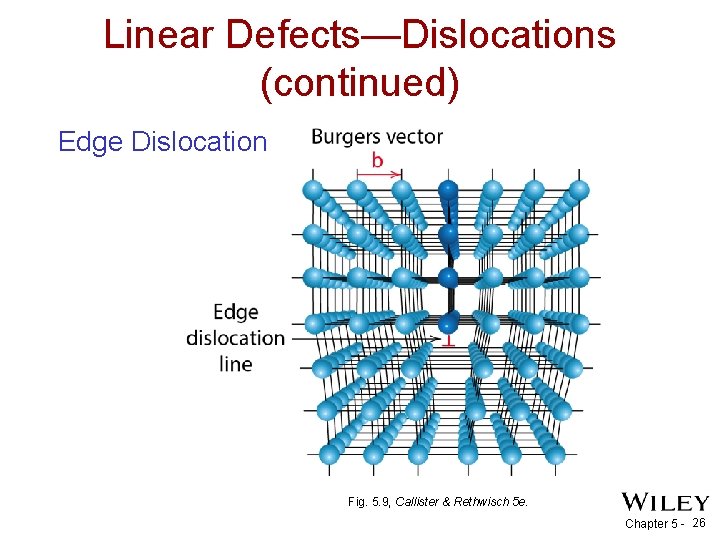
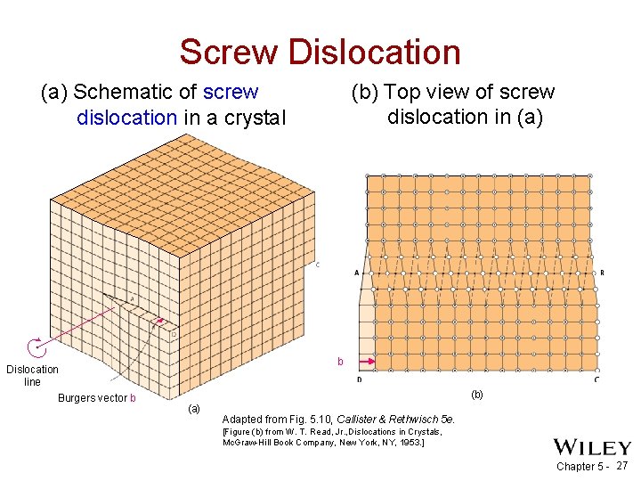
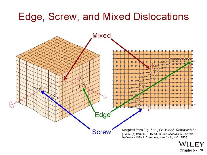
Linear Defects—Dislocations – Are one-dimensional defects around which atoms are misaligned • Edge dislocation: – extra half-plane of atoms inserted in a crystal structure – b perpendicular ( ) to dislocation line • Screw dislocation: – spiral planar ramp resulting from shear deformation – b parallel ( ) to dislocation line Burger’s vector, b: measure of lattice distortion Chapter 5 - 25

Linear Defects—Dislocations (continued) Edge Dislocation Fig. 5. 9, Callister & Rethwisch 5 e. Chapter 5 - 26

Screw Dislocation (b) Top view of screw dislocation in (a) Schematic of screw dislocation in a crystal Screw Dislocation line Burgers vector b b (b) (a) Adapted from Fig. 5. 10, Callister & Rethwisch 5 e. [Figure (b) from W. T. Read, Jr. , Dislocations in Crystals, Mc. Graw-Hill Book Company, New York, NY, 1953. ] Chapter 5 - 27

Edge, Screw, and Mixed Dislocations Mixed Edge Screw Adapted from Fig. 5. 11, Callister & Rethwisch 5 e. [Figure (b) from W. T. Read, Jr. , Dislocations in Crystals, Mc. Graw-Hill Book Company, New York, NY, 1953. ] Chapter 5 - 28

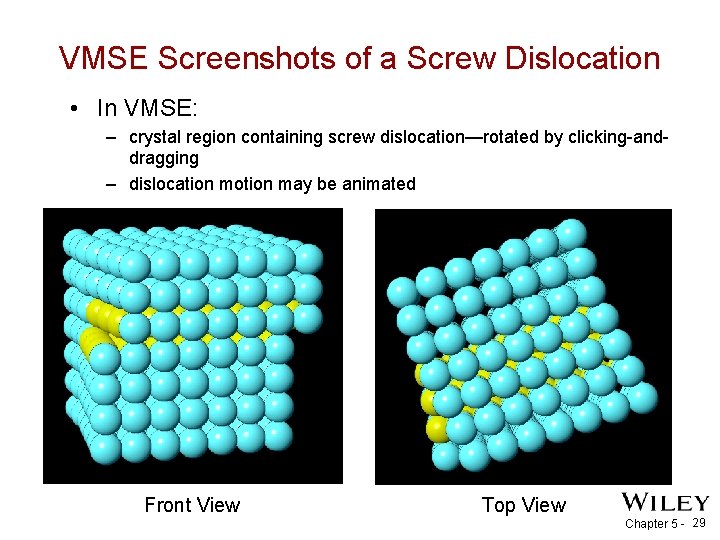
VMSE Screenshots of a Screw Dislocation • In VMSE: – crystal region containing screw dislocation—rotated by clicking-anddragging – dislocation motion may be animated Front View Top View Chapter 5 - 29

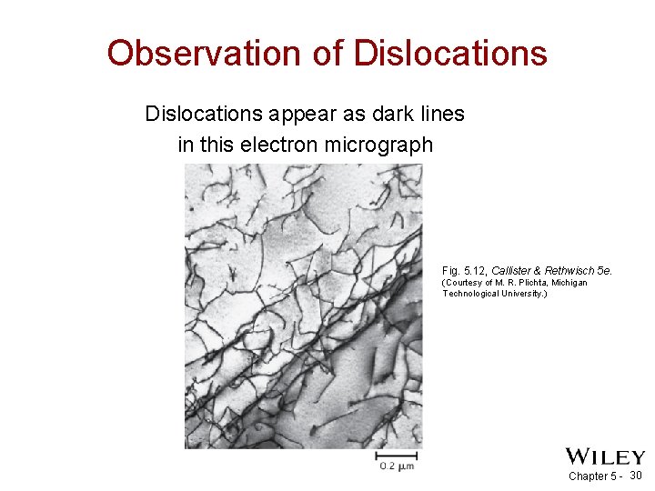
Observation of Dislocations appear as dark lines in this electron micrograph Fig. 5. 12, Callister & Rethwisch 5 e. (Courtesy of M. R. Plichta, Michigan Technological University. ) Chapter 5 - 30

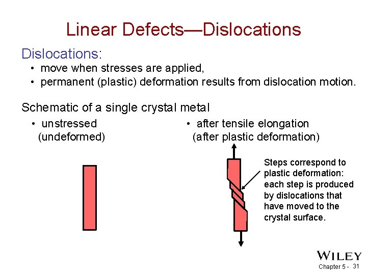
Linear Defects—Dislocations: • move when stresses are applied, • permanent (plastic) deformation results from dislocation motion. Schematic of a single crystal metal • unstressed (undeformed) • after tensile elongation (after plastic deformation) Steps correspond to plastic deformation: each step is produced by dislocations that have moved to the crystal surface. Chapter 5 - 31

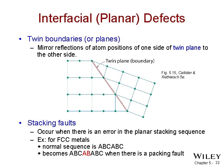
Interfacial (Planar) Defects • Twin boundaries (or planes) – Mirror reflections of atom positions of one side of twin plane to the other side. Fig. 5. 15, Callister & Rethwisch 5 e. • Stacking faults – Occur when there is an error in the planar stacking sequence – Ex: for FCC metals normal sequence is ABCABC becomes ABCABABC when there is a packing fault Chapter 5 - 32

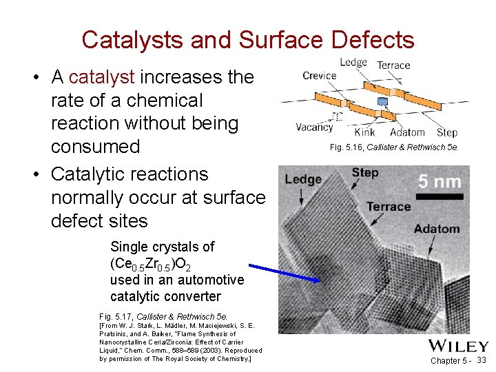
Catalysts and Surface Defects • A catalyst increases the rate of a chemical reaction without being consumed • Catalytic reactions normally occur at surface defect sites Fig. 5. 16, Callister & Rethwisch 5 e. Single crystals of (Ce 0. 5 Zr 0. 5)O 2 used in an automotive catalytic converter Fig. 5. 17, Callister & Rethwisch 5 e. [From W. J. Stark, L. Mädler, M. Maciejewski, S. E. Pratsinis, and A. Baiker, “Flame Synthesis of Nanocrystalline Ceria/Zirconia: Effect of Carrier Liquid, ” Chem. Comm. , 588– 589 (2003). Reproduced by permission of The Royal Society of Chemistry. ] Chapter 5 - 33

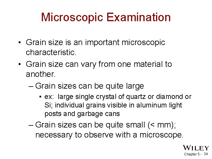
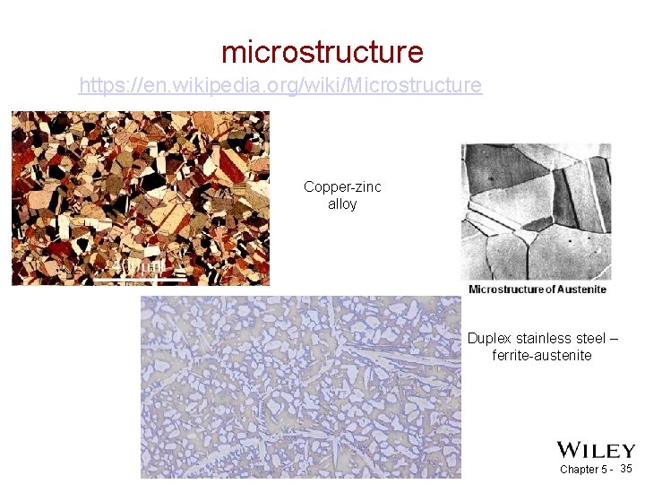
Microscopic Examination • Grain size is an important microscopic characteristic. • Grain size can vary from one material to another. – Grain sizes can be quite large • ex: large single crystal of quartz or diamond or Si; individual grains visible in aluminum light posts and garbage cans – Grain sizes can be quite small (< mm); necessary to observe with a microscope. Chapter 5 - 34

microstructure https: //en. wikipedia. org/wiki/Microstructure Copper-zinc alloy Duplex stainless steel – ferrite-austenite Chapter 5 - 35

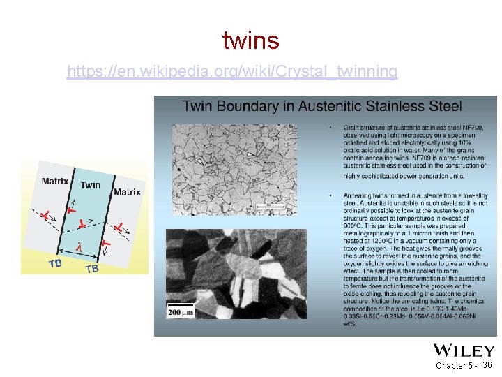
twins https: //en. wikipedia. org/wiki/Crystal_twinning Chapter 5 - 36

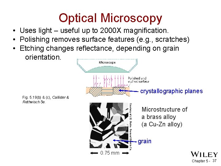
Optical Microscopy • Uses light – useful up to 2000 X magnification. • Polishing removes surface features (e. g. , scratches) • Etching changes reflectance, depending on grain orientation. crystallographic planes 0. 75 mm Courtesy of J. E. Burke, General Electric Co. Fig. 5. 19(b) & (c), Callister & Rethwisch 5 e. Microstructure of a brass alloy (a Cu-Zn alloy) grain Chapter 5 - 37

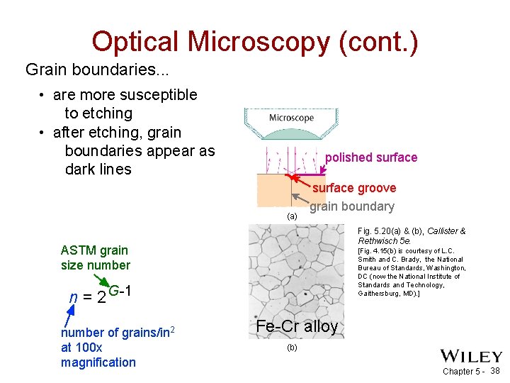
Optical Microscopy (cont. ) Grain boundaries. . . • are more susceptible to etching • after etching, grain boundaries appear as dark lines polished surface (a) surface groove grain boundary Fig. 5. 20(a) & (b), Callister & Rethwisch 5 e. ASTM grain size number [Fig. 4. 15(b) is courtesy of L. C. Smith and C. Brady, the National Bureau of Standards, Washington, DC (now the National Institute of Standards and Technology, Gaithersburg, MD). ] n = 2 G-1 number of grains/in 2 at 100 x magnification Fe-Cr alloy (b) Chapter 5 - 38

Optical Microscopy • Polarized light – metallographic scopes often use polarized light to increase contrast – Also used for transparent samples such as polymers Chapter 5 - 39

Electron Microscopy Best resolution for optical microscopes is ≈ 0. 1 μm (100 nm) For higher resolution need to use shorter wavelength radiation – X-Rays? Difficult to focus. – Electron beams • Wavelengths as short as 3 pm (0. 003 nm) possible – (Magnification as high as 1, 000 X are achievable) • Atomic resolution possible • Electron beams focused by magnetic lenses. Chapter 5 - 40

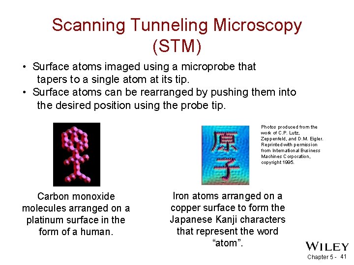
Scanning Tunneling Microscopy (STM) • Surface atoms imaged using a microprobe that tapers to a single atom at its tip. • Surface atoms can be rearranged by pushing them into the desired position using the probe tip. Photos produced from the work of C. P. Lutz, Zeppenfeld, and D. M. Eigler. Reprinted with permission from International Business Machines Corporation, copyright 1995. Carbon monoxide molecules arranged on a platinum surface in the form of a human. Iron atoms arranged on a copper surface to form the Japanese Kanji characters that represent the word “atom”. Chapter 5 - 41

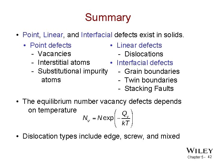
Summary • Point, Linear, and Interfacial defects exist in solids. • Point defects • Linear defects - Vacancies - Dislocations - Interstitial atoms • Interfacial defects - Substitutional impurity - Grain boundaries atoms - Twin boundaries - Stacking Faults • The equilibrium number vacancy defects depends on temperature • Dislocation types include edge, screw, and mixed Chapter 5 - 42

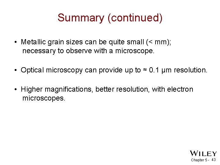
Summary (continued) • Metallic grain sizes can be quite small (< mm); necessary to observe with a microscope. • Optical microscopy can provide up to ≈ 0. 1 μm resolution. • Higher magnifications, better resolution, with electron microscopes. Chapter 5 - 43

ANNOUNCEMENTS Reading: Core Problems: Self-help Problems: Chapter 5 - 44