2 IC Interface Technical Deep Dive March 2018















- Slides: 117

2 IC Interface Technical Deep Dive March 2018 1

TI Training - summary I 2 C Summary: This training will focus on the I 2 C protocol and the challenges our customer designer’s face when using this standard. Topics covered will include basic I 2 C protocol, challenges/tradeoffs of I 2 C, and how TI products help overcome these problems. What you’ll learn: • Learn I 2 C Protocol • Understand I 2 C challenges • Provide solutions to problems 2

Detailed Agenda • Overview of I 2 C – Hardware – Protocol • Devices – – Translators Switches Buffers I/O Expanders 3

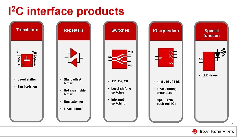
I 2 C interface products Translators Repeaters Switches IO expanders I 2 C 1 I 2 C … IO 1 IO 2 IO 3 Special function I 2 C ION I 2 C 2 • Level-shifter • Bus Isolation • LED driver • Static offset buffer • Hot-swappable buffer • Bus extender • 1: 2, 1: 4, 1: 8 • 4 -, 8 -, 16 -, 24 -bit • Level-shifting switches • Level-shifting expanders • Interrupt switching • Open drain, push-pull IOs • Level-shifter 4

I 2 C Overview Hardware 5

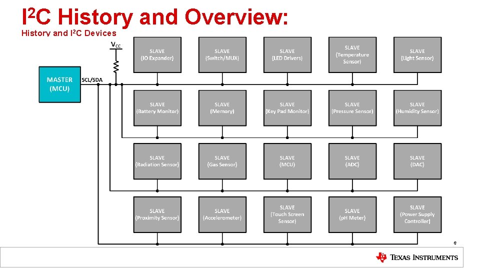
2 IC History and Overview: History and I 2 C Devices 6

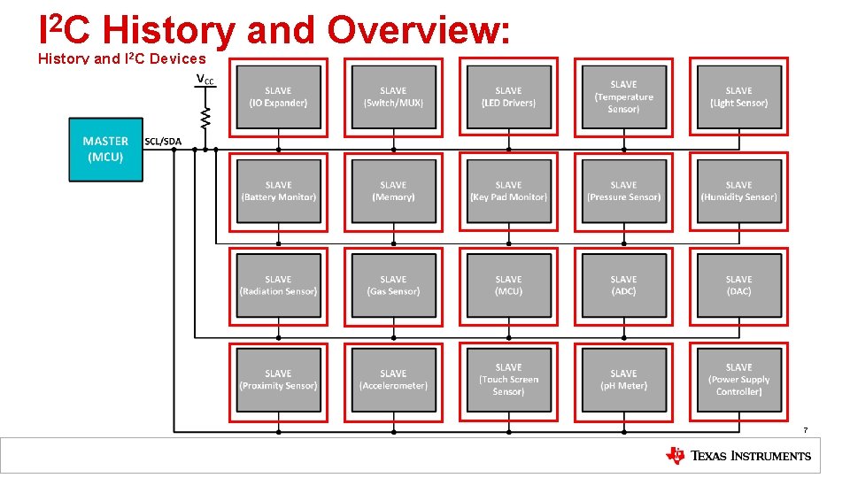
2 IC History and Overview: History and I 2 C Devices 7

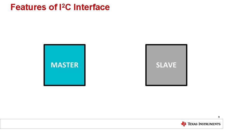
Features of I 2 C Interface 8

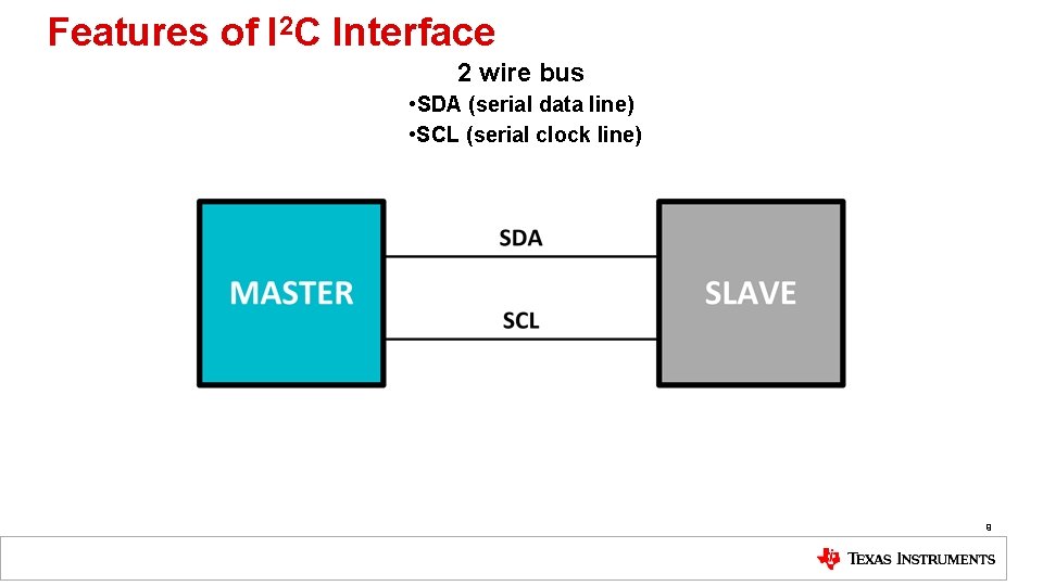
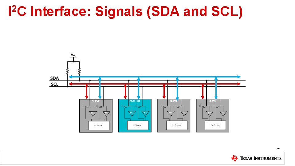
Features of I 2 C Interface 2 wire bus • SDA (serial data line) • SCL (serial clock line) 9

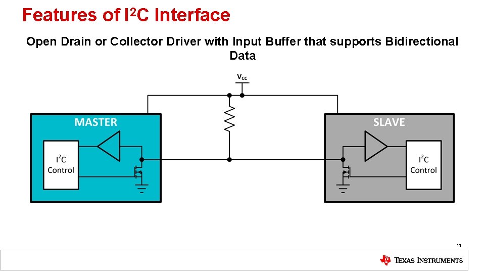
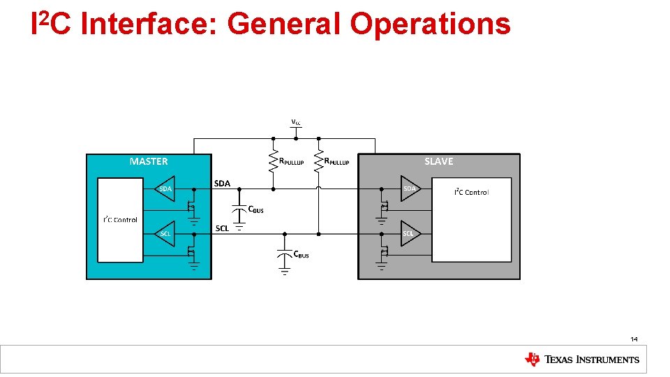
Features of I 2 C Interface Open Drain or Collector Driver with Input Buffer that supports Bidirectional Data 10

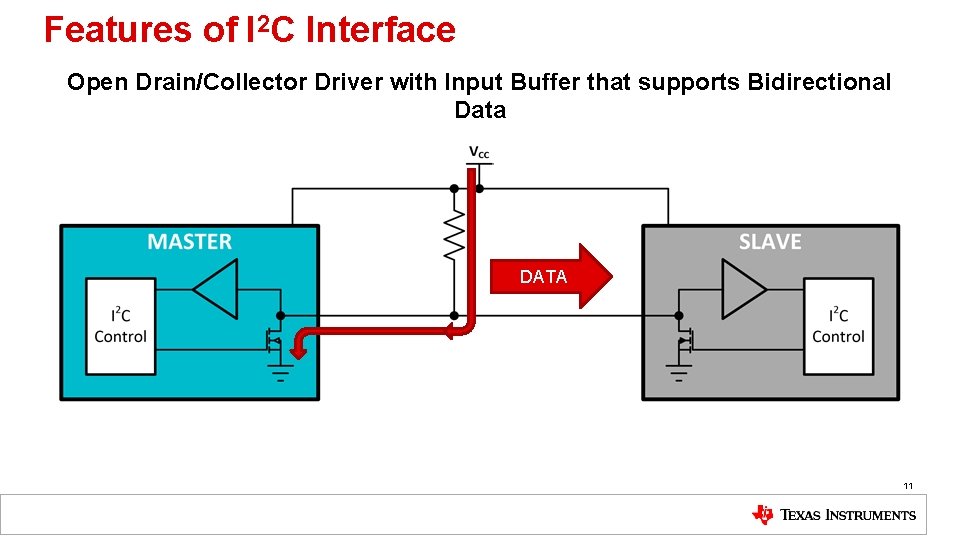
Features of I 2 C Interface Open Drain/Collector Driver with Input Buffer that supports Bidirectional Data DATA 11

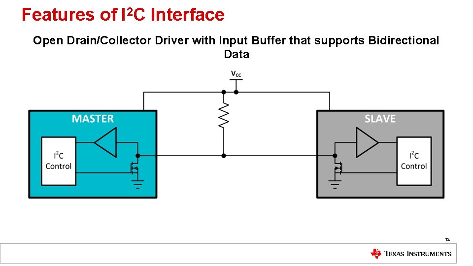
Features of I 2 C Interface Open Drain/Collector Driver with Input Buffer that supports Bidirectional Data 12

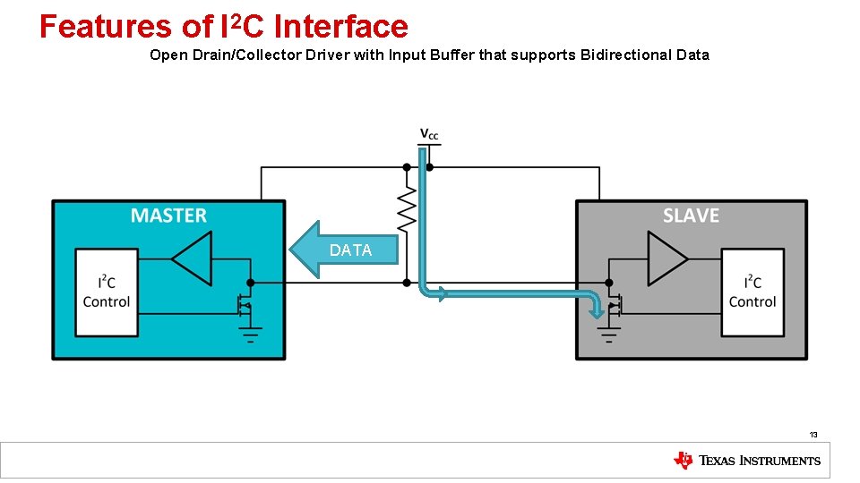
Features of I 2 C Interface Open Drain/Collector Driver with Input Buffer that supports Bidirectional Data DATA 13

2 IC Interface: General Operations 14

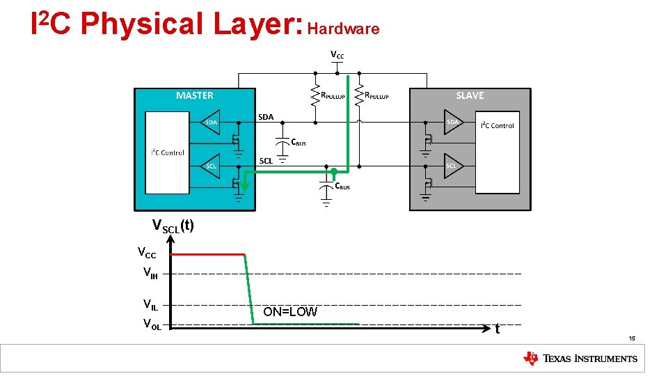
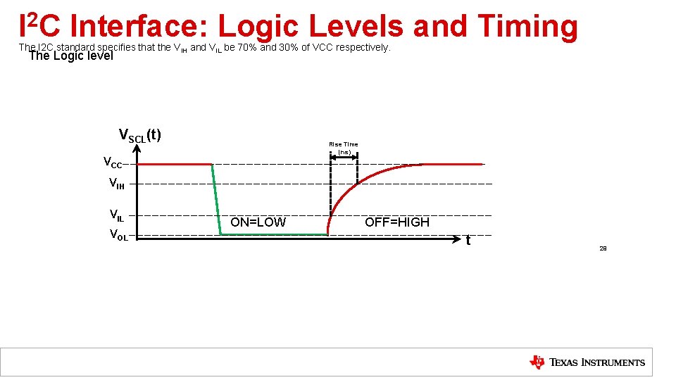
2 IC Physical Layer: Hardware VSCL(t) VCC VIH VIL VOL ON=LOW t 15

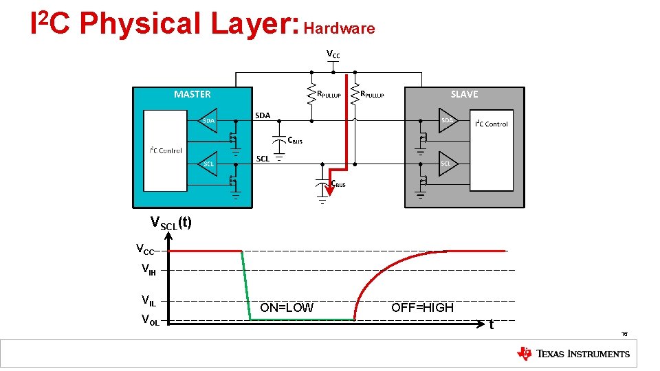
2 IC Physical Layer: Hardware VSCL(t) VCC VIH VIL VOL ON=LOW OFF=HIGH t 16

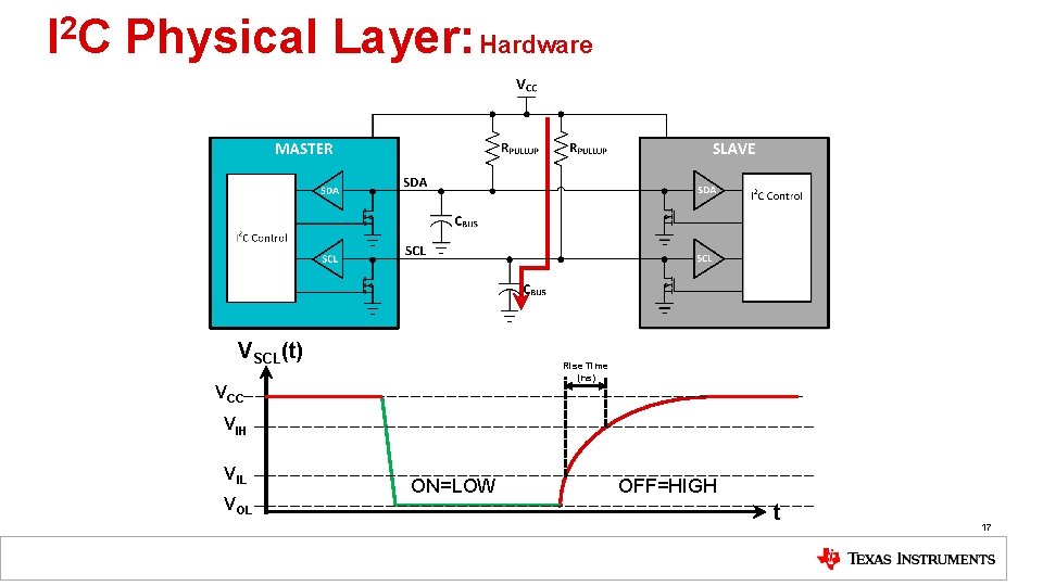
2 IC Physical Layer: Hardware VSCL(t) Rise Time (ns) VCC VIH VIL VOL ON=LOW OFF=HIGH t 17

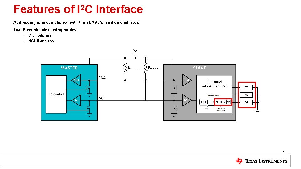
Features of I 2 C Interface Addressing is accomplished with the SLAVE’s hardware address. Two Possible addressing modes: – 7 -bit address – 10 -bit address 18

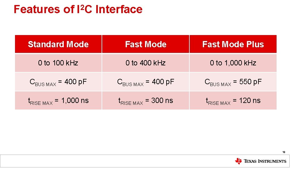
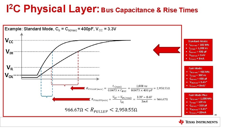
Features of I 2 C Interface Standard Mode Fast Mode Plus 0 to 100 k. Hz 0 to 400 k. Hz 0 to 1, 000 k. Hz CBUS MAX = 400 p. F CBUS MAX = 550 p. F t. RISE MAX = 1, 000 ns t. RISE MAX = 300 ns t. RISE MAX = 120 ns 19

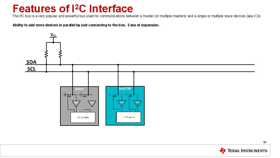
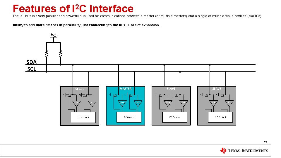
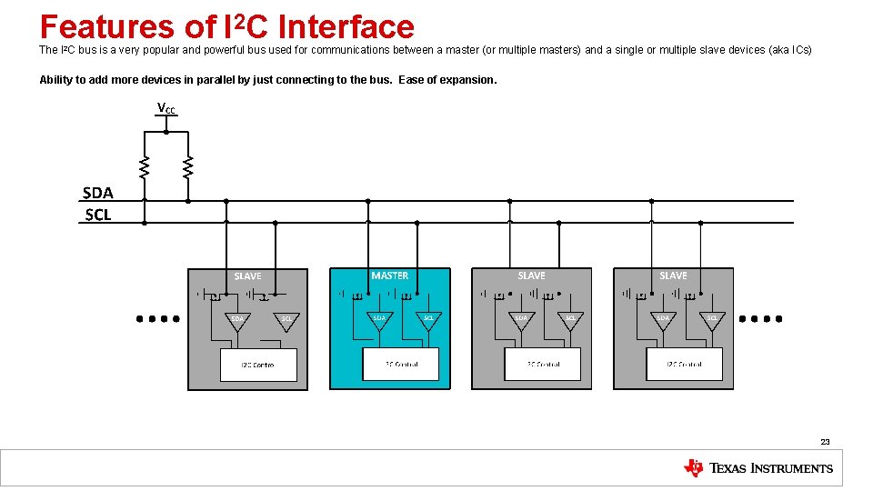
Features of I 2 C Interface The I 2 C bus is a very popular and powerful bus used for communications between a master (or multiple masters) and a single or multiple slave devices (aka ICs) Ability to add more devices in parallel by just connecting to the bus. Ease of expansion. 20

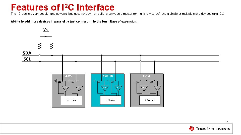
Features of I 2 C Interface The I 2 C bus is a very popular and powerful bus used for communications between a master (or multiple masters) and a single or multiple slave devices (aka ICs) Ability to add more devices in parallel by just connecting to the bus. Ease of expansion. 21

Features of I 2 C Interface The I 2 C bus is a very popular and powerful bus used for communications between a master (or multiple masters) and a single or multiple slave devices (aka ICs) Ability to add more devices in parallel by just connecting to the bus. Ease of expansion. 22

Features of I 2 C Interface The I 2 C bus is a very popular and powerful bus used for communications between a master (or multiple masters) and a single or multiple slave devices (aka ICs) Ability to add more devices in parallel by just connecting to the bus. Ease of expansion. 23

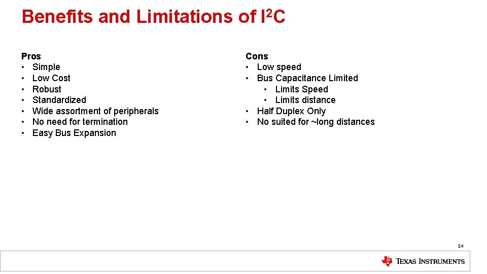
Benefits and Limitations of I 2 C Pros • Simple • Low Cost • Robust • Standardized • Wide assortment of peripherals • No need for termination • Easy Bus Expansion Cons • Low speed • Bus Capacitance Limited • Limits Speed • Limits distance • Half Duplex Only • No suited for ~long distances 24

Benefits and Limitations of I 2 C Pros • Simple • Low Cost • Robust • Standardized • Wide assortment of peripherals • No need for termination • Easy Bus Expansion Cons • Low speed • Bus Capacitance Limited • Limits Speed • Limits distance • Half Duplex Only • No suited for ~long distances 25

I 2 C Overview Protocol 26

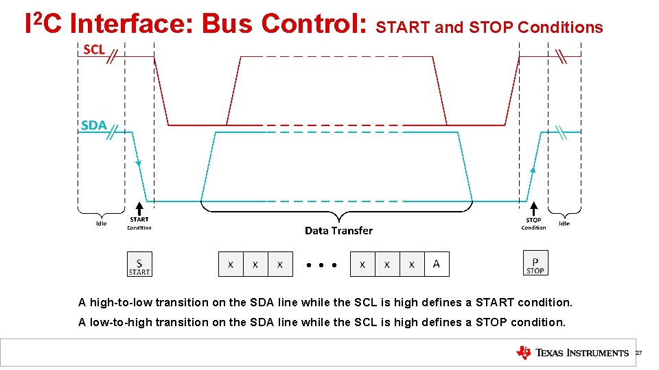
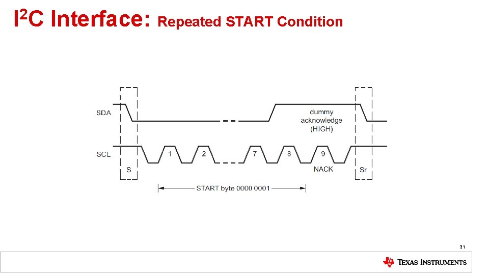
I 2 C Interface: Bus Control: START and STOP Conditions A high-to-low transition on the SDA line while the SCL is high defines a START condition. A low-to-high transition on the SDA line while the SCL is high defines a STOP condition. 27

I 2 C Interface: Signals (SDA and SCL) 28

I 2 C Interface: Logic Levels and Timing The I 2 C standard specifies that the VIH and VIL be 70% and 30% of VCC respectively. The Logic level VSCL(t) Rise Time (ns) VCC VIH VIL VOL ON=LOW OFF=HIGH t 29

I 2 C Interface: Byte Format 30

I 2 C Interface: Repeated START Condition 31

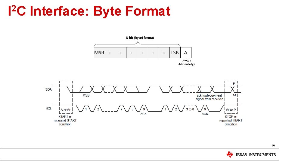
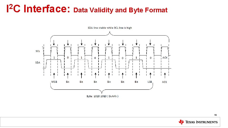
I 2 C Interface: Data Validity and Byte Format 32

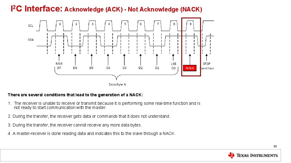
I 2 C Interface: Acknowledge (ACK) - Not Acknowledge (NACK) There are several conditions that lead to the generation of a NACK: 1. The receiver is unable to receive or transmit because it is performing some real-time function and is not ready to start communication with the master. 2. During the transfer, the receiver gets data or commands that it does not understand. 3. During the transfer, the receiver cannot receive any more data bytes. 4. A master-receiver is done reading data and indicates this to the slave through a NACK. 33

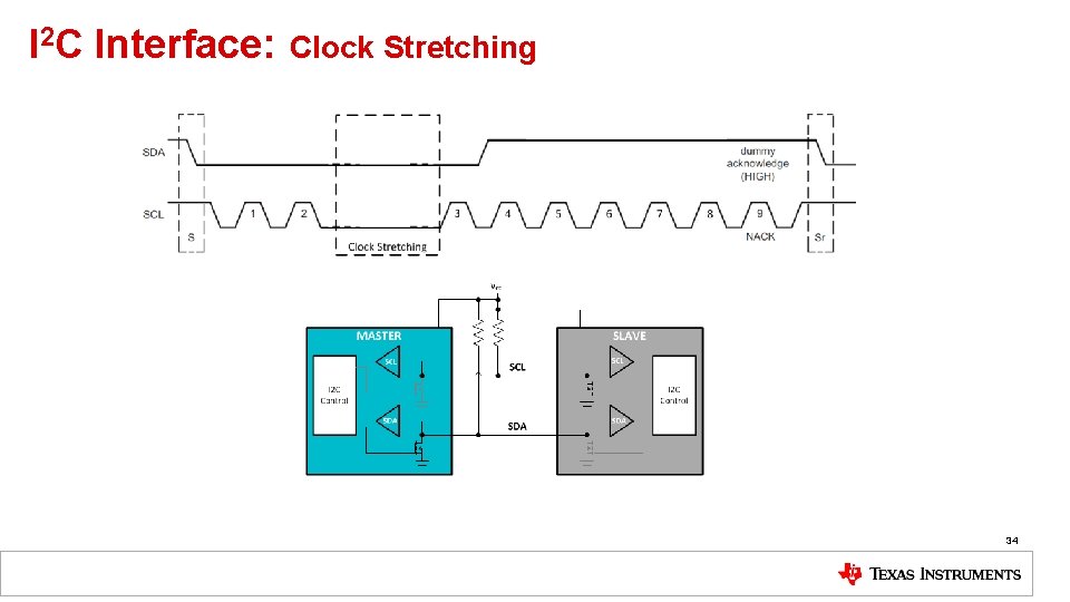
I 2 C Interface: Clock Stretching 34

I 2 C Interface: Other I 2 C Based Protocols • System Management Bus (SMBUS) • Power Management Bus (PMBUS) • Intelligent Platform Management Interface (IPMI) • Display Data Channel (DDC) • Advanced Telecom Computing Architecture (ATCA) 35

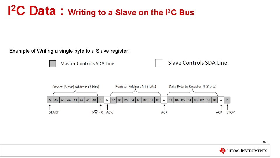
I 2 C Data : Writing to a Slave on the I 2 C Bus Example of Writing a single byte to a Slave register: 36

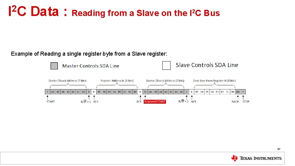
I 2 C Data : Reading from a Slave on the I 2 C Bus Example of Reading a single register byte from a Slave register: 37

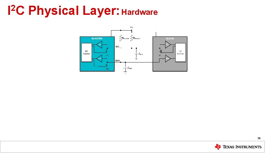
I 2 C Physical Layer: Hardware 38

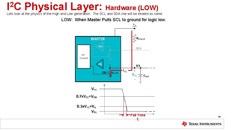
I 2 C Physical Layer: Hardware (LOW) Lets look at the physics of the High and Low generation. The SCL and SDA line will be treated as same. LOW: When Master Pulls SCL to ground for logic low. IOL + VOL _ Fall Time tf 39

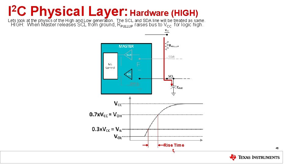
I 2 C Physical Layer: Hardware (HIGH) Lets look at the physics of the High and Low generation. The SCL and SDA line will be treated as same. HIGH: When Master releases SCL from ground, RPULLUP raises bus to VCC for logic high. Rise Time tr 40

I 2 C Physical Layer: Bus Capacitance & Rise Times Example: Standard Mode, Cb = Cb(max) = 400 p. F, VCC = 3. 3 V 41

Translators 42

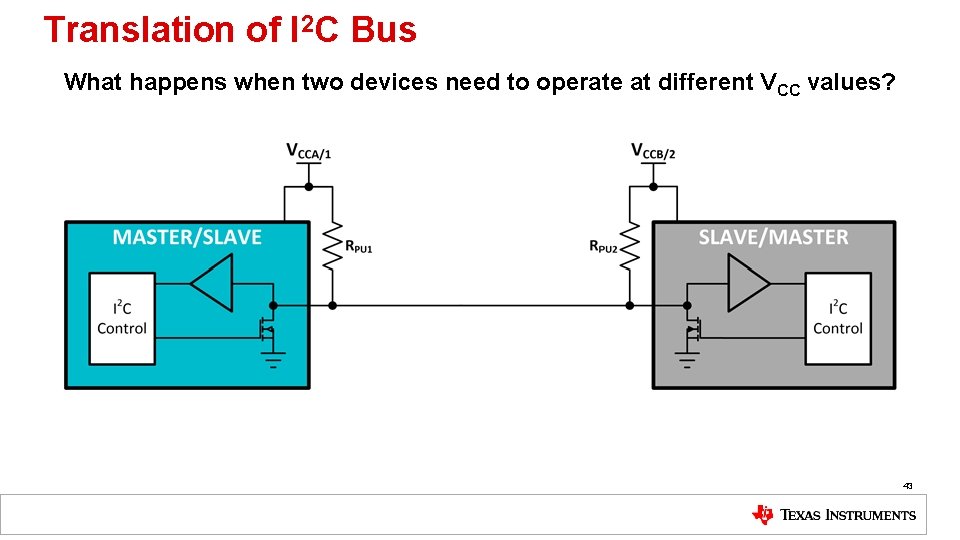
Translation of I 2 C Bus What happens when two devices need to operate at different V CC values? 43

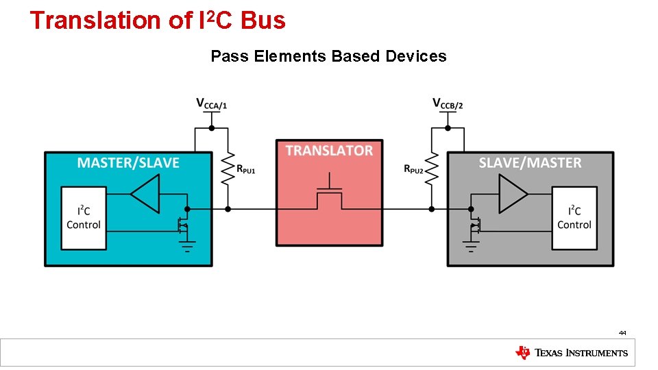
Translation of I 2 C Bus Pass Elements Based Devices 44

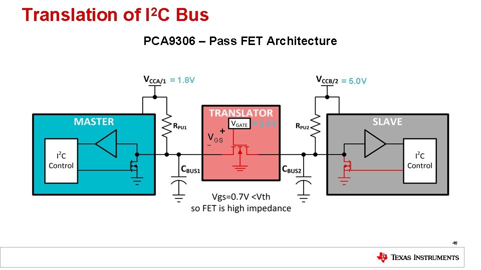
Translation of I 2 C Bus PCA 9306 – Pass FET Architecture = 1. 8 V = 5. 0 V + _VGS 45

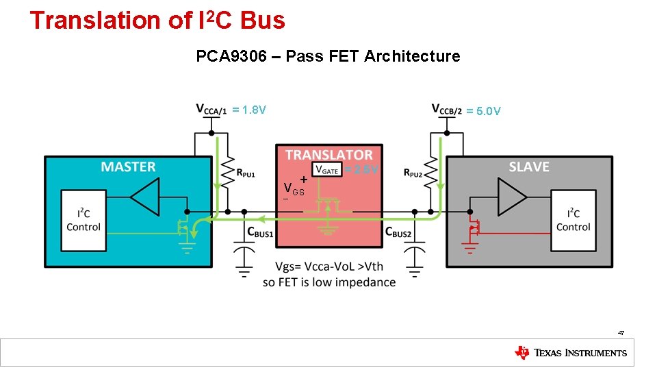
Translation of I 2 C Bus PCA 9306 – Pass FET Architecture = 1. 8 V = 5. 0 V + V _ GS = 2. 5 V 46

Translation of I 2 C Bus PCA 9306 – Pass FET Architecture = 1. 8 V = 5. 0 V + V _ GS = 2. 5 V 47

Translation of I 2 C Bus PCA 9306 – Pass FET Architecture = 1. 8 V = 5. 0 V 48

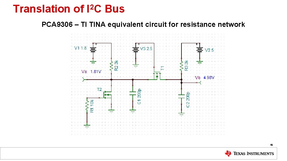
Translation of I 2 C Bus PCA 9306 – TI TINA equivalent circuit for resistance network 49

Translation of I 2 C Bus PCA 9306 – Pass FET Architecture = 1. 8 V = 5. 0 V + V _ GS = 2. 5 V 50

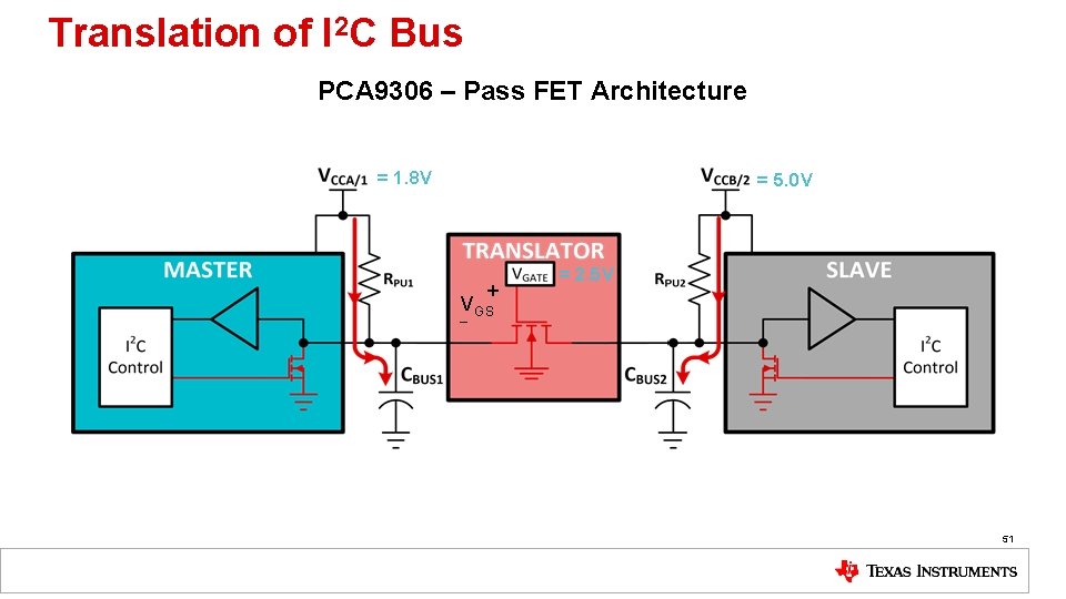
Translation of I 2 C Bus PCA 9306 – Pass FET Architecture = 1. 8 V = 5. 0 V + V _ GS = 2. 5 V 51

Translation/Level Shifting of I 2 C Bus Design Considerations: • Translators introduce propagation delays – Delays become longer the further Vref 1 and Vref 2 are from each other • Example: if Vref 1 and Vref 2 difference is 3 V, propagation delays will be lower if Vref 1 and Vref 2 at 1 V – Placing Translators in series will further increase propagation delays and could cause timing issues – Higher gate voltages will lower propagation delays • Translators will not buffer capacitance on both sides of the translator. 52

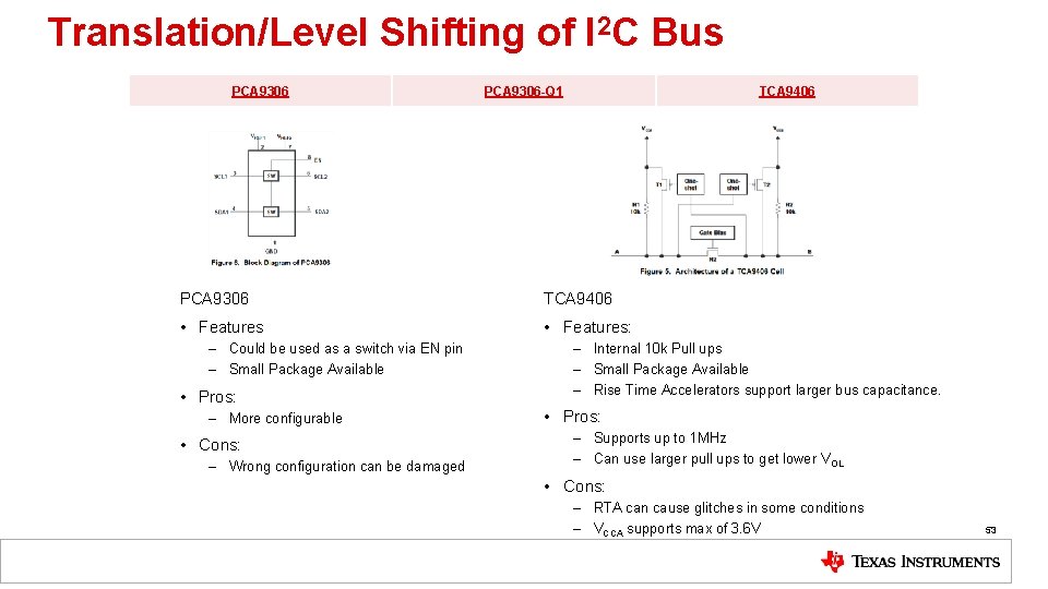
Translation/Level Shifting of I 2 C Bus PCA 9306 -Q 1 TCA 9406 PCA 9306 TCA 9406 • Features: – Could be used as a switch via EN pin – Small Package Available • Pros: – More configurable • Cons: – Wrong configuration can be damaged – Internal 10 k Pull ups – Small Package Available – Rise Time Accelerators support larger bus capacitance. • Pros: – Supports up to 1 MHz – Can use larger pull ups to get lower VOL • Cons: – RTA can cause glitches in some conditions – VCCA supports max of 3. 6 V 53

Translators Common questions 54

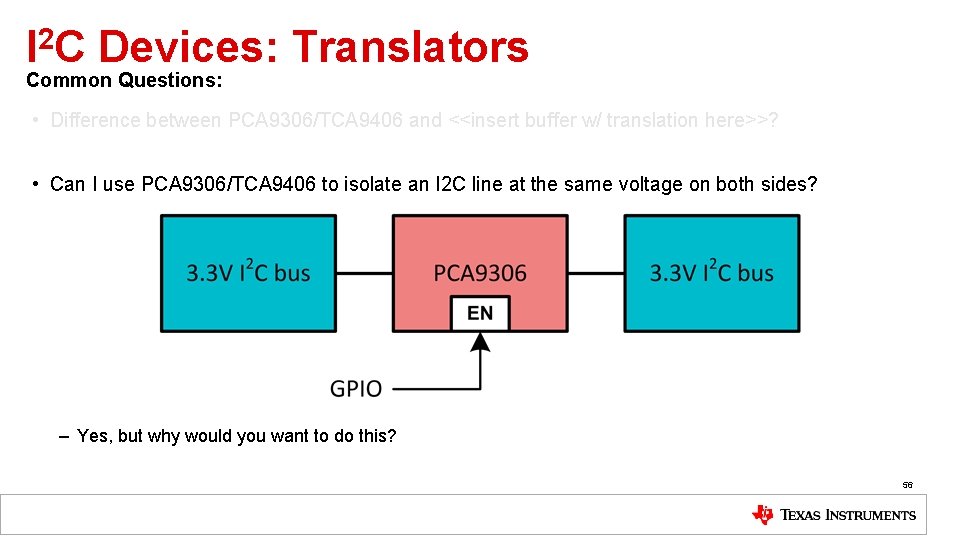
I 2 C Devices: Translators Common Question: • Difference between PCA 9306/TCA 9406 and <<insert buffer w/ translation here>>? – PCA 9306/TCA 9406 do not provide active buffering because it is a pass FET architecture. – Buffers typically have an offset on one side and PCA 9306/TCA 9406 pass Vo. L to the opposite side with little voltage increase due to voltage drop due to pass FET resistance and pull down current. 55

I 2 C Devices: Translators Common Questions: • Difference between PCA 9306/TCA 9406 and <<insert buffer w/ translation here>>? • Can I use PCA 9306/TCA 9406 to isolate an I 2 C line at the same voltage on both sides? • Does master need to be on side 1 of the device? – Yes, but why would you want to do this? 56

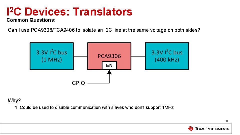
I 2 C Devices: Translators Common Questions: Can I use PCA 9306/TCA 9406 to isolate an I 2 C line at the same voltage on both sides? • Does master need to be on side 1 of the device? Why? 1. Could be used to disable communication with slaves who don’t support 1 MHz 57

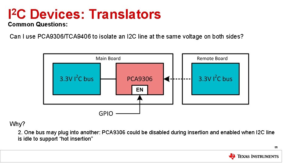
I 2 C Devices: Translators Common Questions: Can I use PCA 9306/TCA 9406 to isolate an I 2 C line at the same voltage on both sides? Why? 2. One bus may plug into another: PCA 9306 could be disabled during insertion and enabled when I 2 C line is idle to support “hot insertion” 58

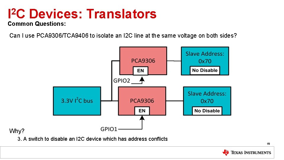
I 2 C Devices: Translators Common Questions: Can I use PCA 9306/TCA 9406 to isolate an I 2 C line at the same voltage on both sides? Why? 3. A switch to disable an I 2 C device which has address conflicts 59

I 2 C Devices: Translators Common Question: • Difference between PCA 9306/TCA 9406 and <<insert buffer w/ translation here>>? • Can I use PCA 9306/TCA 9406 to isolate a I 2 C line at the same voltage on both sides? • Does master need to be on side 1 of the device? (The datasheet pictures show master only on side 1) – Both PCA 9306 and TCA 9406 are Bidirectional and do not know/care which side master is on 60

Switches 61

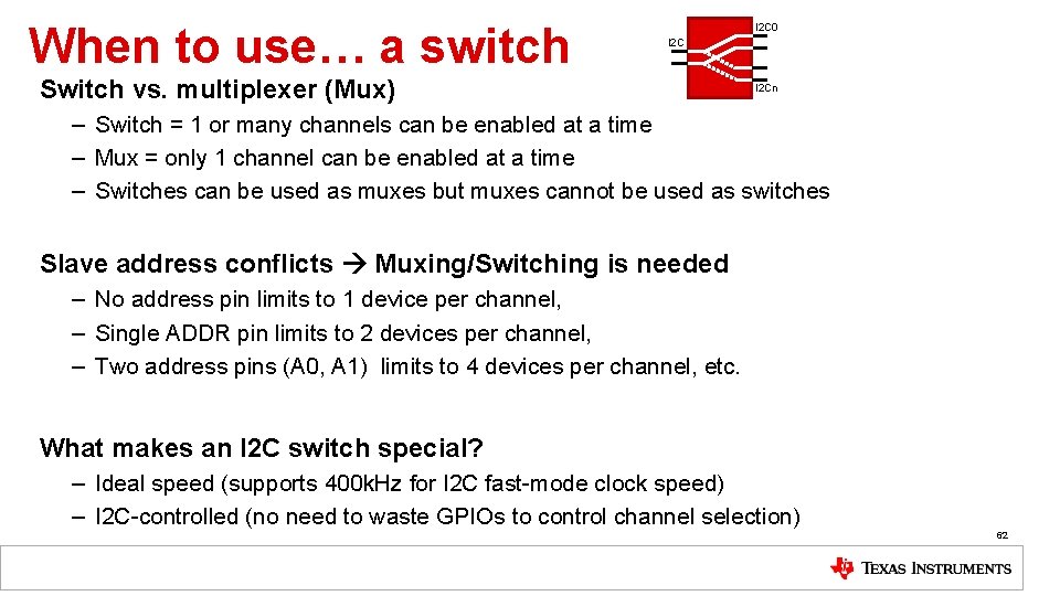
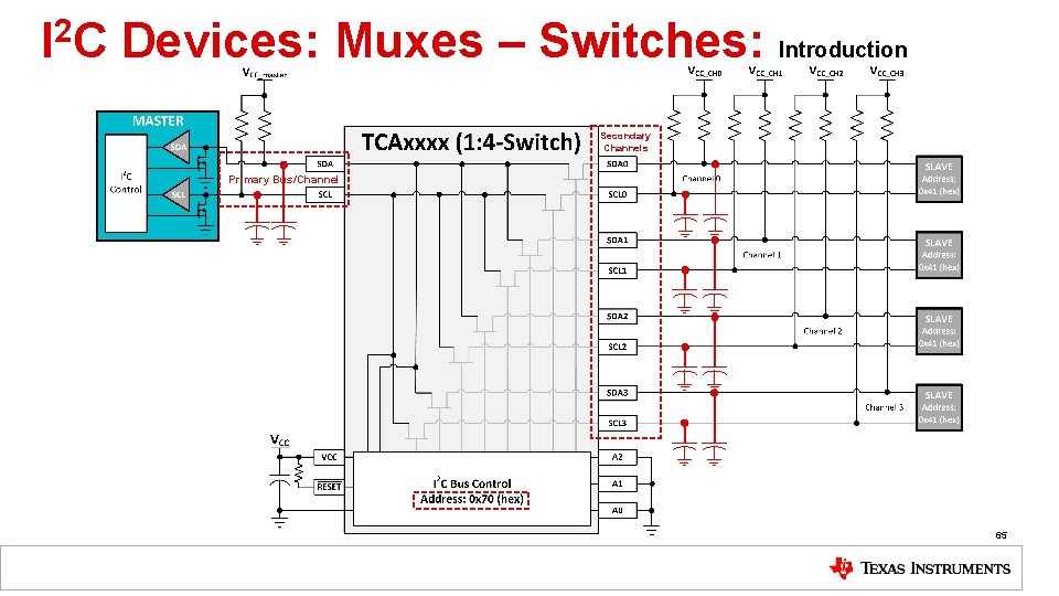
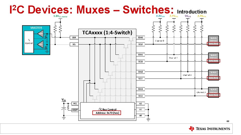
When to use… a switch I 2 C 0 I 2 C Switch vs. multiplexer (Mux) I 2 Cn – Switch = 1 or many channels can be enabled at a time – Mux = only 1 channel can be enabled at a time – Switches can be used as muxes but muxes cannot be used as switches Slave address conflicts Muxing/Switching is needed – No address pin limits to 1 device per channel, – Single ADDR pin limits to 2 devices per channel, – Two address pins (A 0, A 1) limits to 4 devices per channel, etc. What makes an I 2 C switch special? – Ideal speed (supports 400 k. Hz for I 2 C fast-mode clock speed) – I 2 C-controlled (no need to waste GPIOs to control channel selection) 62

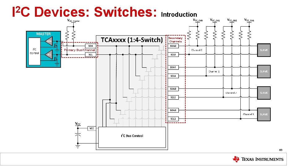
I 2 C Devices: Switches: Introduction Secondary Channels Primary Bus/Channel 63

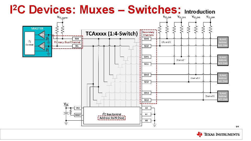
2 IC Devices: Muxes – Switches: Introduction Secondary Channels Primary Bus/Channel 64

I 2 C Devices: Muxes – Switches: Introduction Secondary Channels Primary Bus/Channel 65

I 2 C Devices: Muxes – Switches: Introduction 66

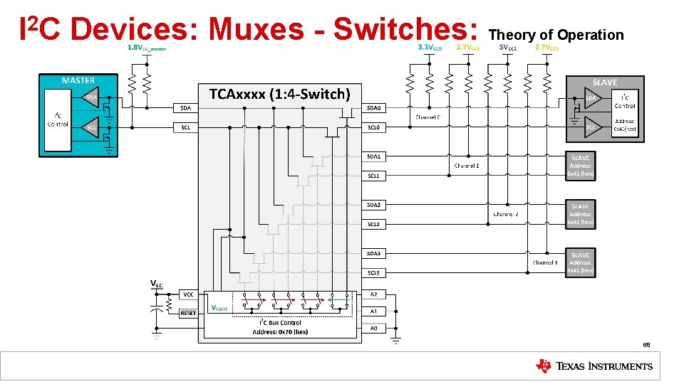
2 IC Devices: Muxes - Switches: Theory of Operation 67

2 IC Devices: Muxes - Switches: Theory of Operation 68

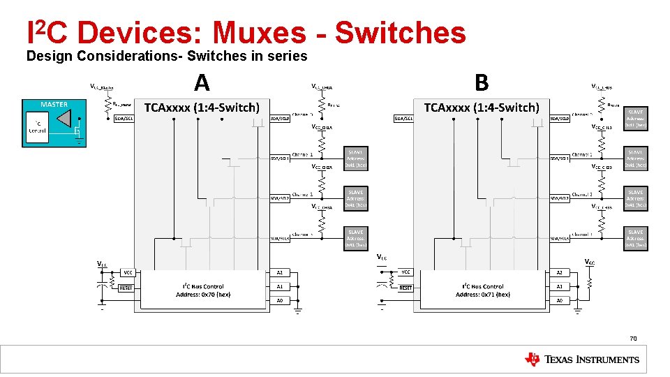
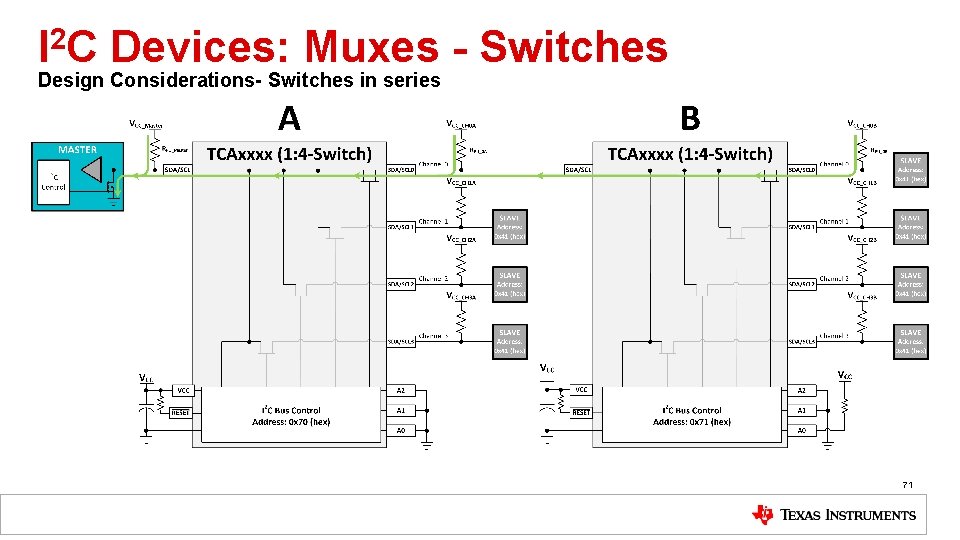
Switches Design Considerations Switches in Series 69

I 2 C Devices: Muxes - Switches Design Considerations- Switches in series 70

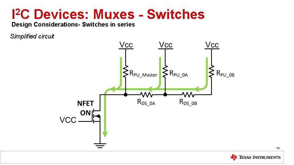
I 2 C Devices: Muxes - Switches Design Considerations- Switches in series 71

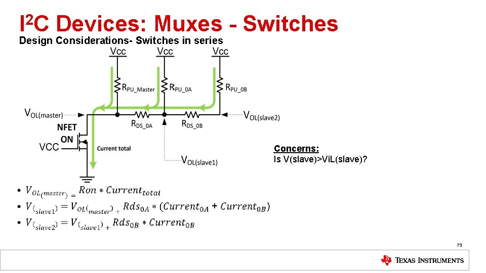
I 2 C Devices: Muxes - Switches Design Considerations- Switches in series Simplified circuit 72

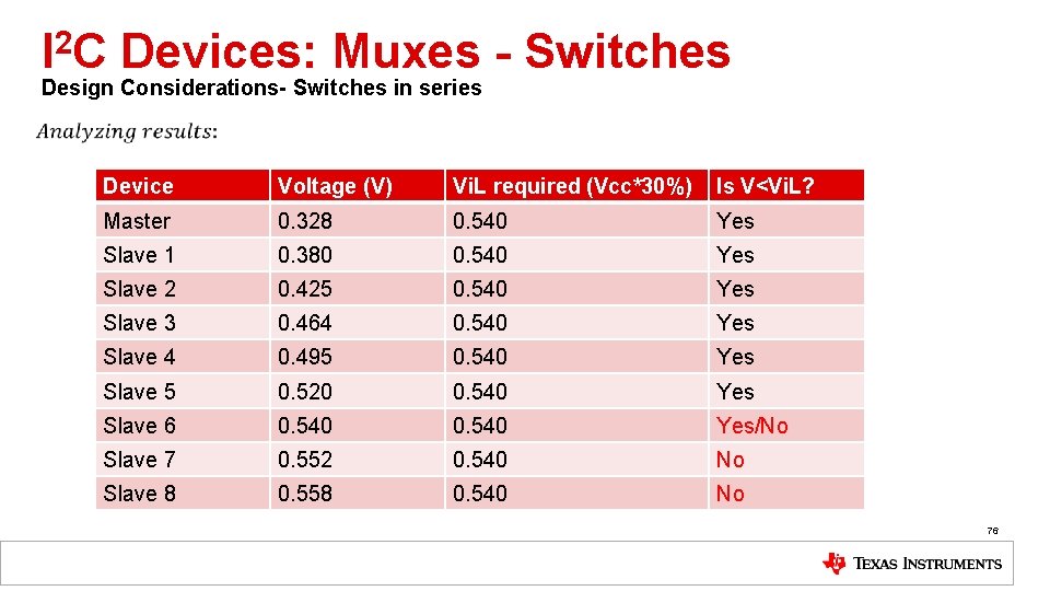
I 2 C Devices: Muxes - Switches Design Considerations- Switches in series Concerns: Is V(slave)>Vi. L(slave)? 73

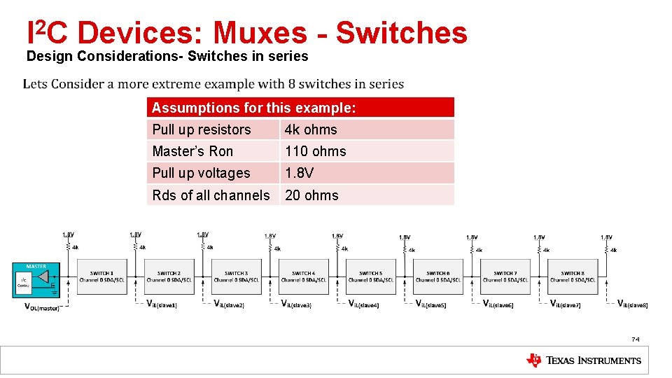
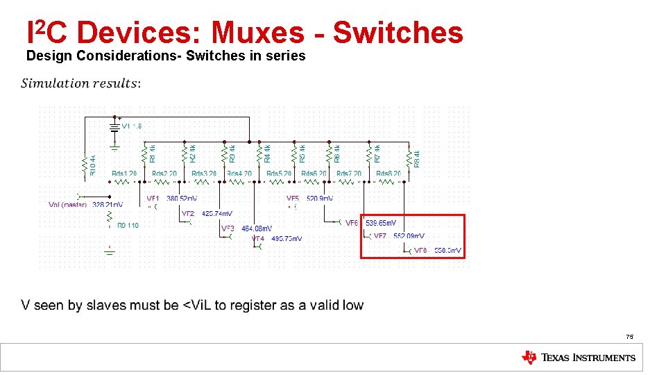
I 2 C Devices: Muxes - Switches Design Considerations- Switches in series Assumptions for this example: Pull up resistors 4 k ohms Master’s Ron 110 ohms Pull up voltages 1. 8 V Rds of all channels 20 ohms 74

I 2 C Devices: Muxes - Switches Design Considerations- Switches in series 75

I 2 C Devices: Muxes - Switches Design Considerations- Switches in series Device Voltage (V) Vi. L required (Vcc*30%) Is V<Vi. L? Master 0. 328 0. 540 Yes Slave 1 0. 380 0. 540 Yes Slave 2 0. 425 0. 540 Yes Slave 3 0. 464 0. 540 Yes Slave 4 0. 495 0. 540 Yes Slave 5 0. 520 0. 540 Yes Slave 6 0. 540 Yes/No Slave 7 0. 552 0. 540 No Slave 8 0. 558 0. 540 No 76

Switches Design Considerations Switches in Parallel 77

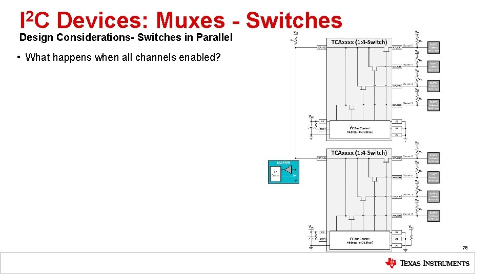
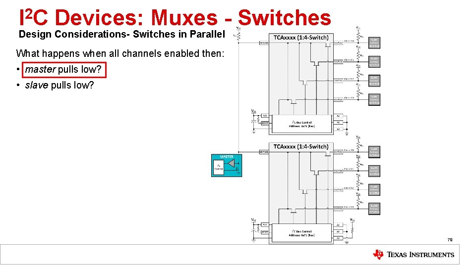
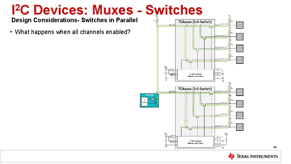
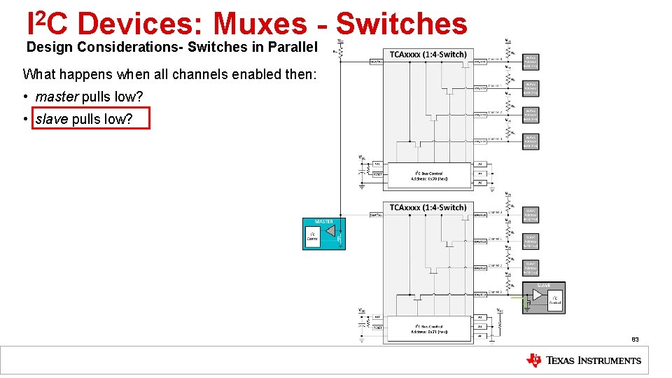
I 2 C Devices: Muxes - Switches Design Considerations- Switches in Parallel • What happens when all channels enabled? 78

I 2 C Devices: Muxes - Switches Design Considerations- Switches in Parallel What happens when all channels enabled then: • master pulls low? • slave pulls low? 79

I 2 C Devices: Muxes - Switches Design Considerations- Switches in Parallel • What happens when all channels enabled? 80

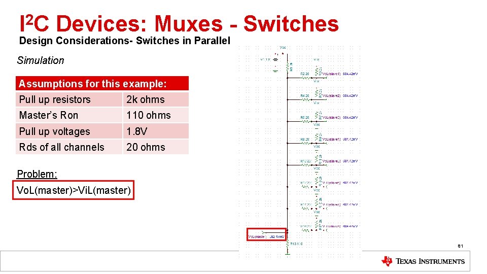
I 2 C Devices: Muxes - Switches Design Considerations- Switches in Parallel Simulation Assumptions for this example: Pull up resistors 2 k ohms Master’s Ron 110 ohms Pull up voltages 1. 8 V Rds of all channels 20 ohms Problem: Vo. L(master)>Vi. L(master) 81

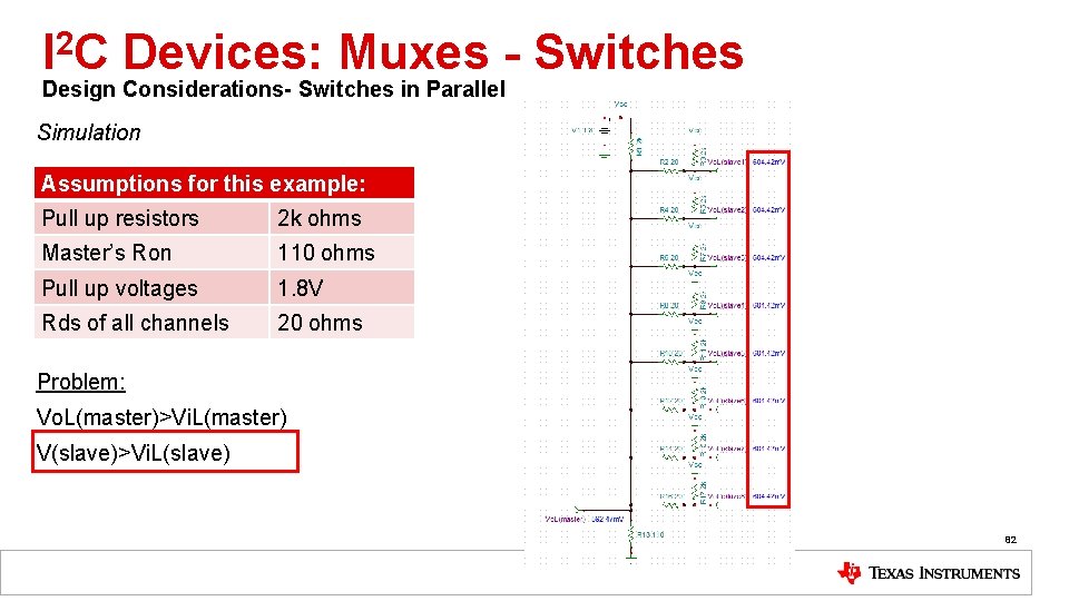
I 2 C Devices: Muxes - Switches Design Considerations- Switches in Parallel Simulation Assumptions for this example: Pull up resistors 2 k ohms Master’s Ron 110 ohms Pull up voltages 1. 8 V Rds of all channels 20 ohms Problem: Vo. L(master)>Vi. L(master) V(slave)>Vi. L(slave) 82

I 2 C Devices: Muxes - Switches Design Considerations- Switches in Parallel What happens when all channels enabled then: • master pulls low? • slave pulls low? 83

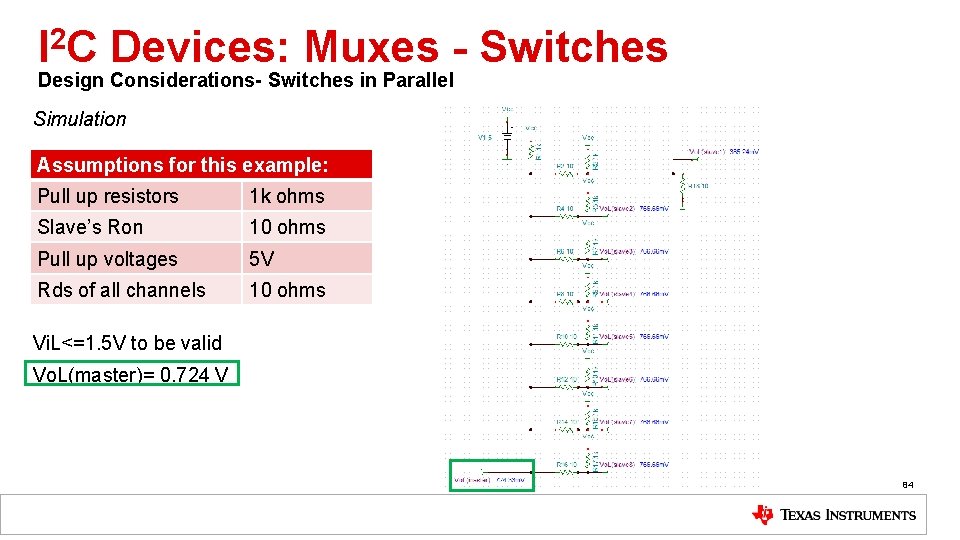
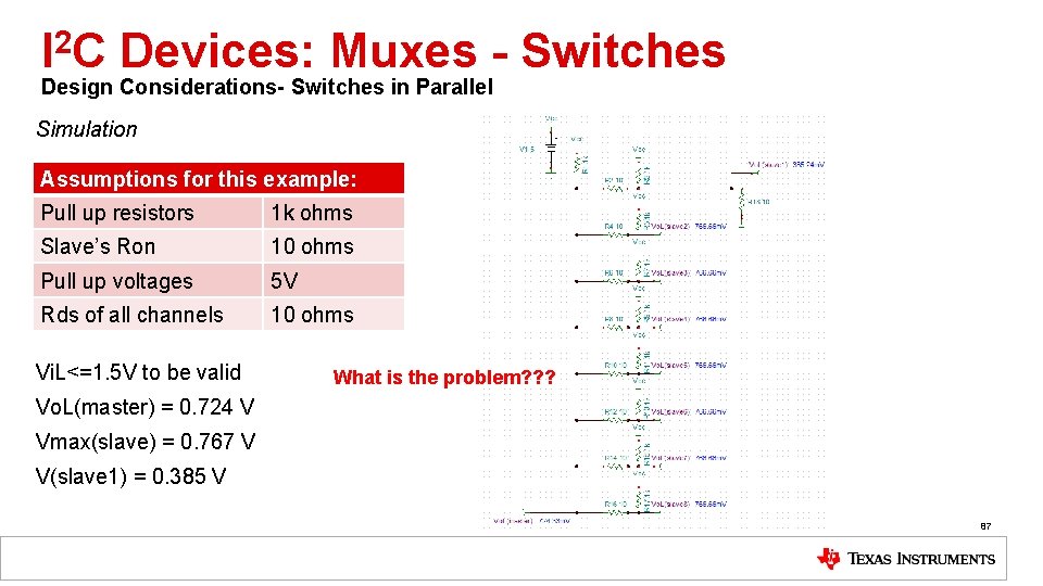
I 2 C Devices: Muxes - Switches Design Considerations- Switches in Parallel Simulation Assumptions for this example: Pull up resistors 1 k ohms Slave’s Ron 10 ohms Pull up voltages 5 V Rds of all channels 10 ohms Vi. L<=1. 5 V to be valid Vo. L(master)= 0. 724 V 84

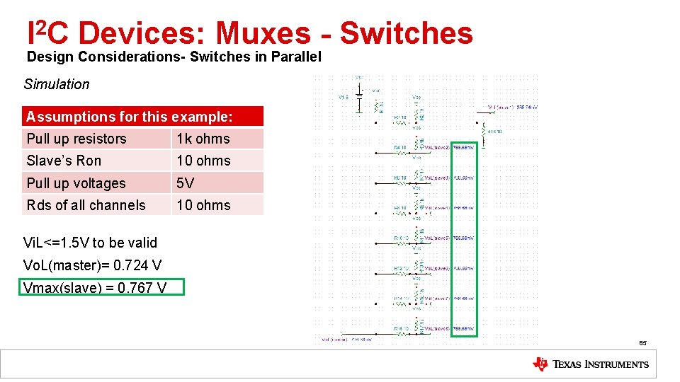
I 2 C Devices: Muxes - Switches Design Considerations- Switches in Parallel Simulation Assumptions for this example: Pull up resistors 1 k ohms Slave’s Ron 10 ohms Pull up voltages 5 V Rds of all channels 10 ohms Vi. L<=1. 5 V to be valid Vo. L(master)= 0. 724 V Vmax(slave) = 0. 767 V 85

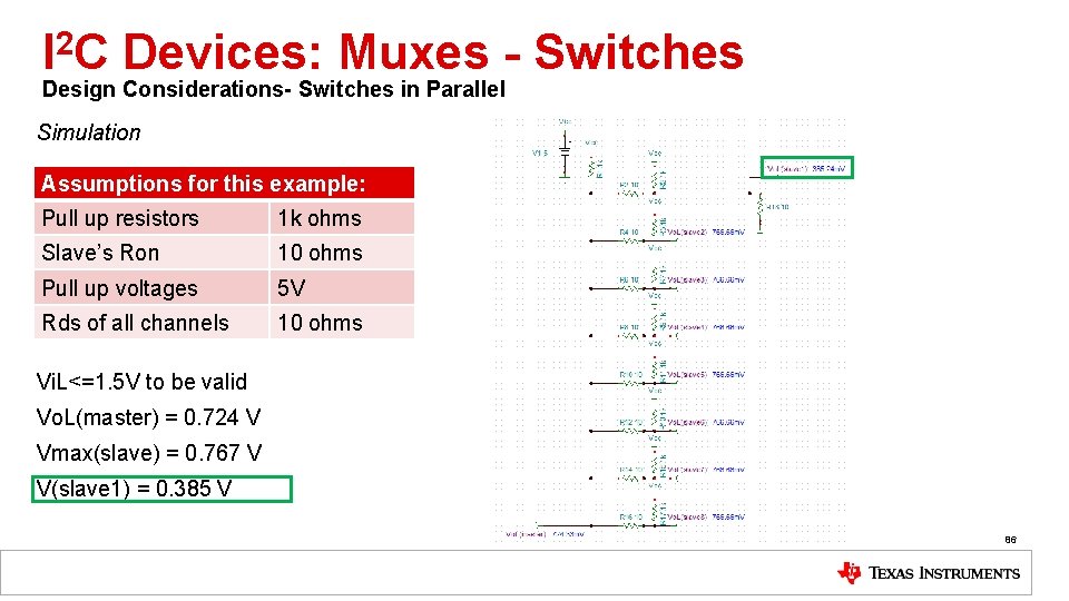
I 2 C Devices: Muxes - Switches Design Considerations- Switches in Parallel Simulation Assumptions for this example: Pull up resistors 1 k ohms Slave’s Ron 10 ohms Pull up voltages 5 V Rds of all channels 10 ohms Vi. L<=1. 5 V to be valid Vo. L(master) = 0. 724 V Vmax(slave) = 0. 767 V V(slave 1) = 0. 385 V 86

I 2 C Devices: Muxes - Switches Design Considerations- Switches in Parallel Simulation Assumptions for this example: Pull up resistors 1 k ohms Slave’s Ron 10 ohms Pull up voltages 5 V Rds of all channels 10 ohms Vi. L<=1. 5 V to be valid What is the problem? ? ? Vo. L(master) = 0. 724 V Vmax(slave) = 0. 767 V V(slave 1) = 0. 385 V 87

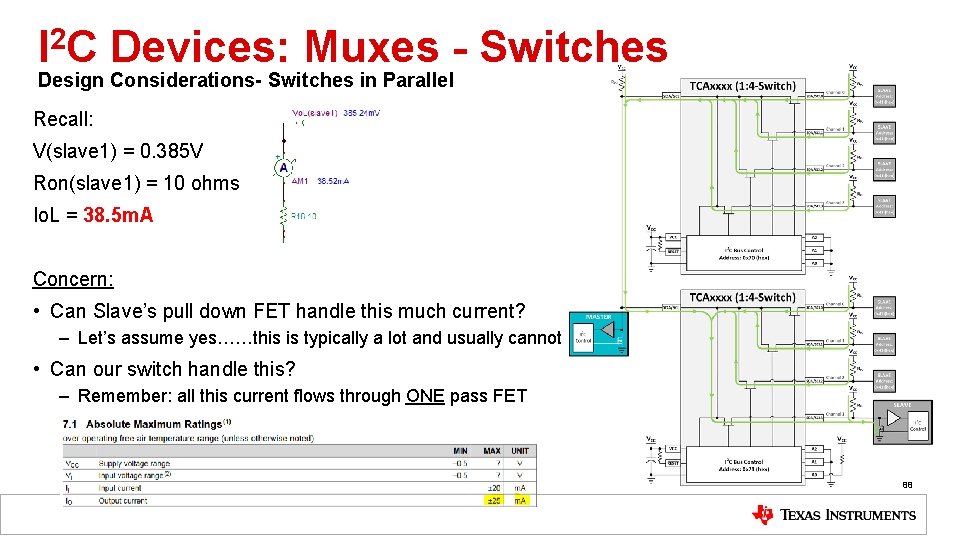
I 2 C Devices: Muxes - Switches Design Considerations- Switches in Parallel Recall: V(slave 1) = 0. 385 V Ron(slave 1) = 10 ohms Io. L = 38. 5 m. A Concern: • Can Slave’s pull down FET handle this much current? – Let’s assume yes……this is typically a lot and usually cannot • Can our switch handle this? – Remember: all this current flows through ONE pass FET 88

Switches Common Questions 89

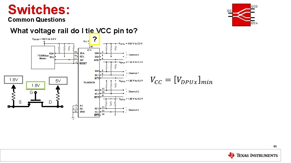
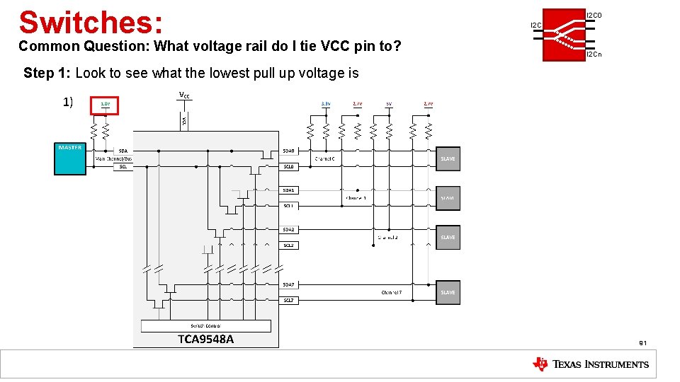
Switches: I 2 C 0 I 2 C Common Questions I 2 Cn What voltage rail do I tie VCC pin to? ? V 1. 8 V DPUM V 5 V DPU 0 1. 8 V V 5 V CC G S D 90

Switches: Common Question: What voltage rail do I tie VCC pin to? I 2 C 0 I 2 Cn Step 1: Look to see what the lowest pull up voltage is 91

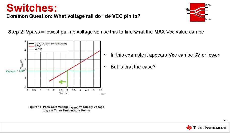
Switches: I 2 C 0 I 2 C Common Question: What voltage rail do I tie VCC pin to? I 2 Cn Step 2: Vpass = lowest pull up voltage so use this to find what the MAX Vcc value can be • In this example it appears Vcc can be 3 V or lower • But is that the case? 92

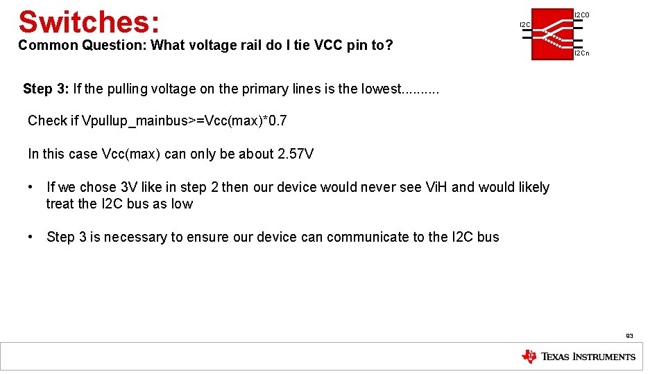
Switches: I 2 C 0 I 2 C Common Question: What voltage rail do I tie VCC pin to? I 2 Cn Step 3: If the pulling voltage on the primary lines is the lowest. . Check if Vpullup_mainbus>=Vcc(max)*0. 7 In this case Vcc(max) can only be about 2. 57 V • If we chose 3 V like in step 2 then our device would never see Vi. H and would likely treat the I 2 C bus as low • Step 3 is necessary to ensure our device can communicate to the I 2 C bus 93

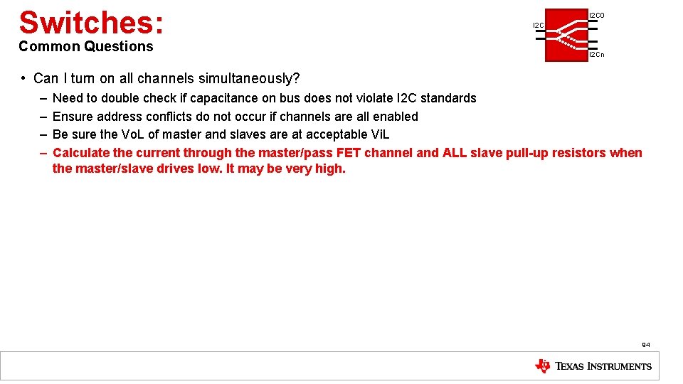
Switches: Common Questions I 2 C 0 I 2 Cn • Can I turn on all channels simultaneously? – – Need to double check if capacitance on bus does not violate I 2 C standards Ensure address conflicts do not occur if channels are all enabled Be sure the Vo. L of master and slaves are at acceptable Vi. L Calculate the current through the master/pass FET channel and ALL slave pull-up resistors when the master/slave drives low. It may be very high. 94

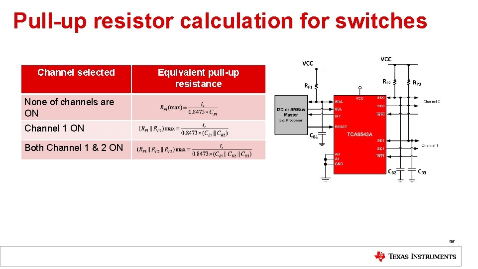
Pull-up resistor calculation for switches Channel selected Equivalent pull-up resistance None of channels are ON Channel 1 ON Both Channel 1 & 2 ON 95

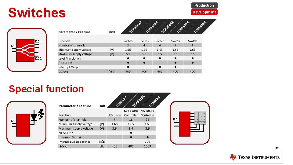
Production Switches Development I 2 C 1 I 2 C 2 Special function I 2 C 1 2 3 4 5 6 7 8 9 * 0 # 96

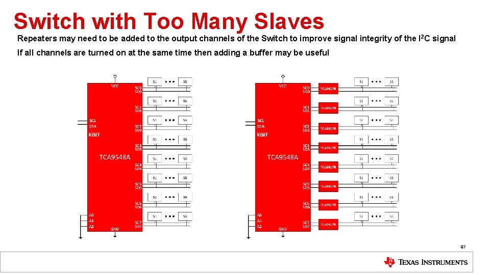
Switch with Too Many Slaves Repeaters may need to be added to the output channels of the Switch to improve signal integrity of the I 2 C signal If all channels are turned on at the same time then adding a buffer may be useful 97

Buffers 98

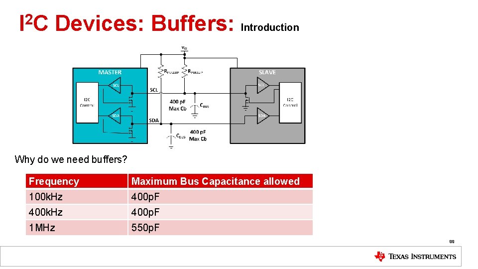
I 2 C Devices: Buffers: Introduction Why do we need buffers? Frequency Maximum Bus Capacitance allowed 100 k. Hz 400 p. F 400 k. Hz 400 p. F 1 MHz 550 p. F 99

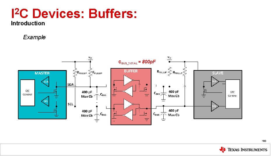
I 2 C Devices: Buffers: Introduction Example CBUS_TOTAL = 800 p. F 100

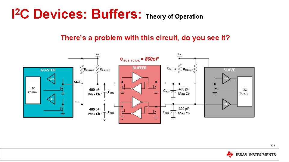
I 2 C Devices: Buffers: Theory of Operation There’s a problem with this circuit, do you see it? CBUS_TOTAL = 800 p. F 101

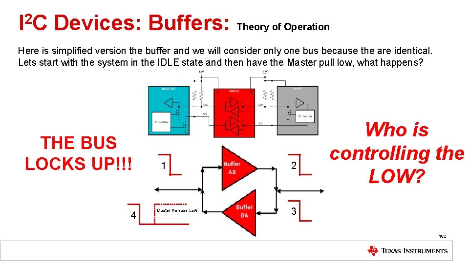
I 2 C Devices: Buffers: Theory of Operation Here is simplified version the buffer and we will consider only one bus because the are identical. Lets start with the system in the IDLE state and then have the Master pull low, what happens? THE BUS LOCKS UP!!! 4 1 Master Release Low 2 Who is controlling the LOW? 3 102

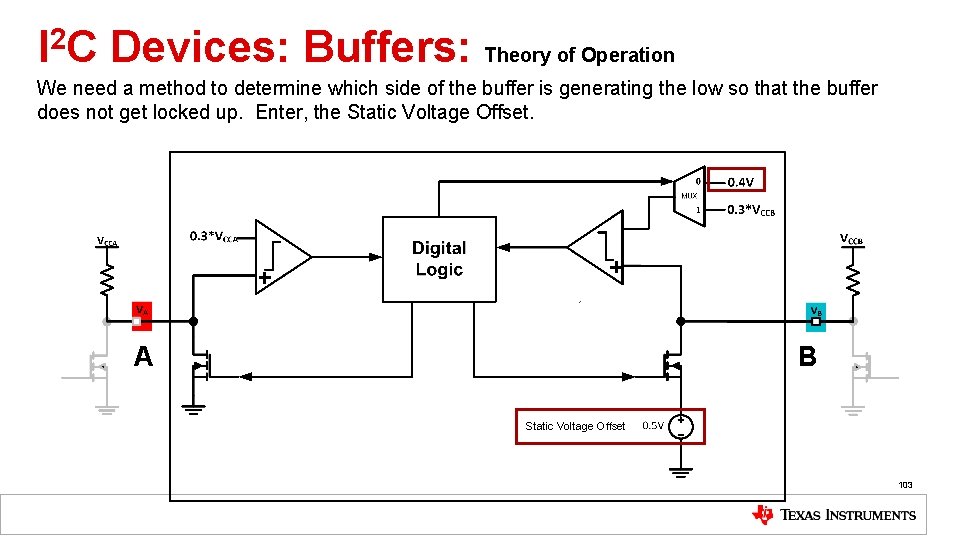
I 2 C Devices: Buffers: Theory of Operation We need a method to determine which side of the buffer is generating the low so that the buffer does not get locked up. Enter, the Static Voltage Offset. B A Static Voltage Offset 103

Buffers Design Considerations 104

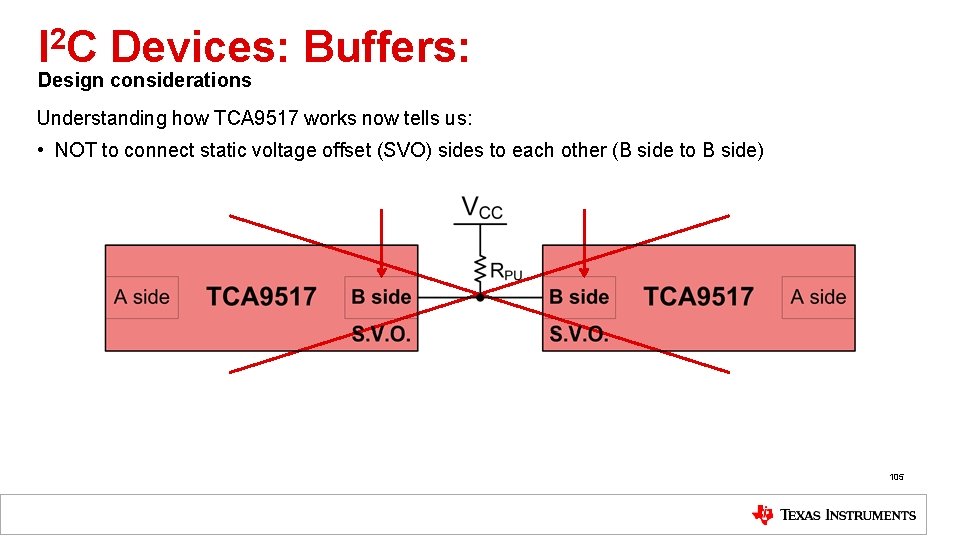
I 2 C Devices: Buffers: Design considerations Understanding how TCA 9517 works now tells us: • NOT to connect static voltage offset (SVO) sides to each other (B side to B side) 105

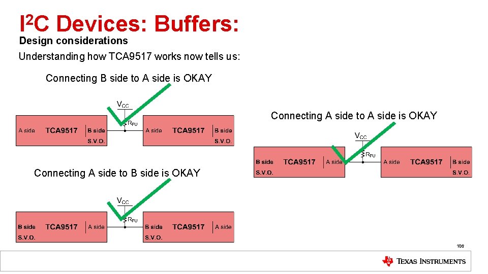
I 2 C Devices: Buffers: Design considerations Understanding how TCA 9517 works now tells us: Connecting B side to A side is OKAY Connecting A side to B side is OKAY 106

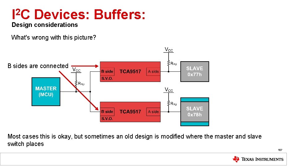
I 2 C Devices: Buffers: Design considerations What's wrong with this picture? B sides are connected Most cases this is okay, but sometimes an old design is modified where the master and slave switch places 107

I 2 C Devices: Buffers: Design Considerations Are there other buffer devices on the bus? – Sides with static voltage offsets should not be connected to each other Are there devices with low Vi. L? – The Vos of buffers can sometimes be larger than Vi. L Can you stack buffers in series? – Yes but there are concerns with this What are the considerations for using buffers in parallel? – Offset sides should still not be connected 108

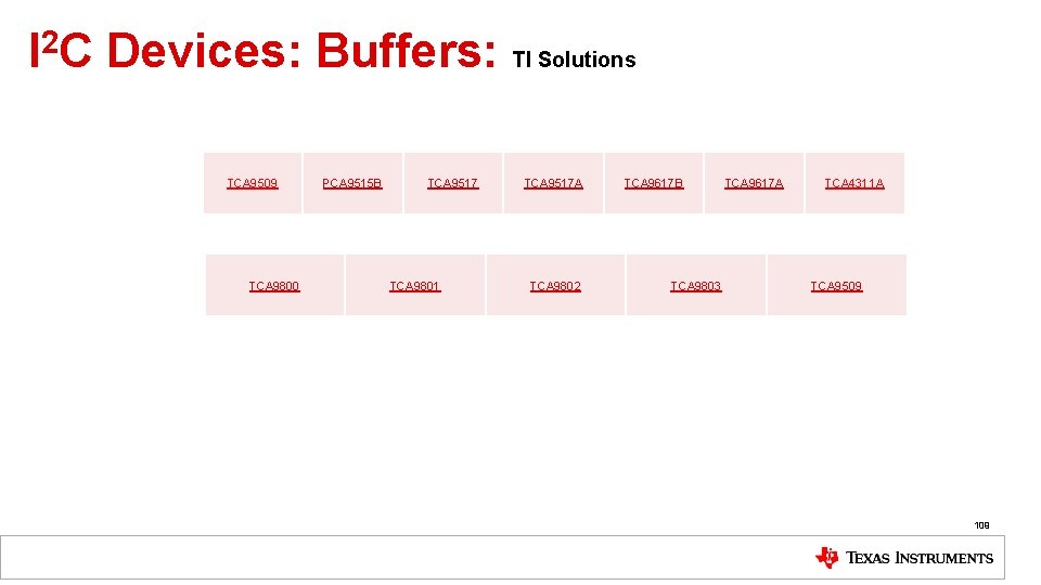
I 2 C Devices: Buffers: TI Solutions TCA 9509 TCA 9800 PCA 9515 B TCA 9517 TCA 9801 TCA 9517 A TCA 9802 TCA 9617 B TCA 9803 TCA 9617 A TCA 4311 A TCA 9509 109

I/O Expanders 110

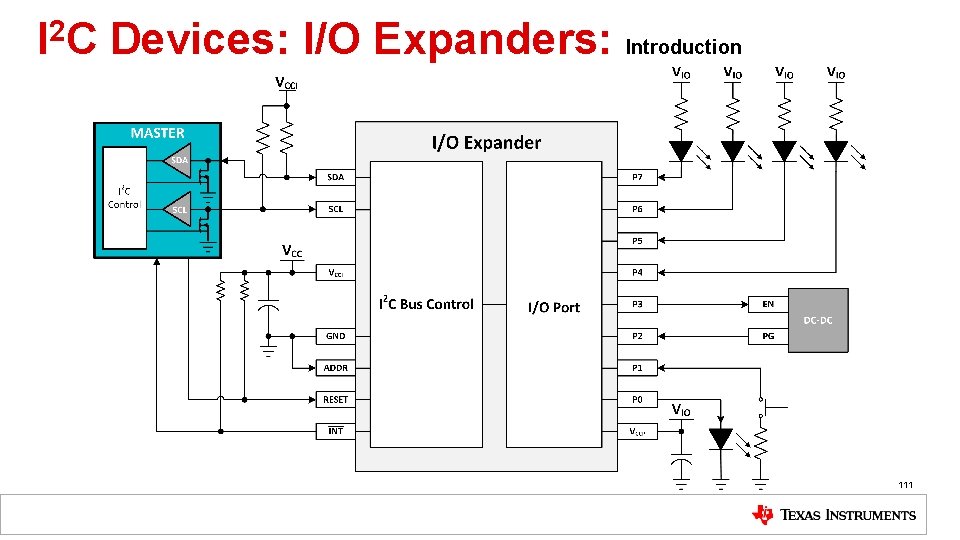
I 2 C Devices: I/O Expanders: Introduction 111

I 2 C Devices: I/O Expanders: Introduction 112

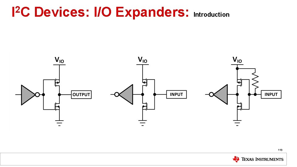
I 2 C Devices: I/O Expanders: Introduction 113

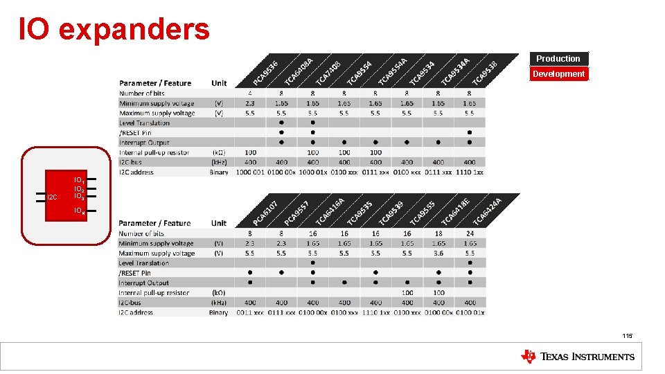
Other FAQs on IO expanders Do the address pins have to pulled HIGH or LOW using a resistor? – It is not a requirement to use a resistor for pulling HIGH or LOW. However, a resistor can be used. Does TI offer IO expander with stuck bus recovery? – We do not have an IO expander with stuck bus recovery feature today. The master need to issue as Reset command or power cycle What is the maximum frequency that the P-port toggle at? – To write to a port you need to send 3 bytes plus the 3 ACK’s and the Start and Stop. So the maximum switching frequency of the Pports can be ~15 k. Hz What is the maximum current you can sink through an 8 -bit IO expander – The recommended current through each port is 10 m. A, and the maximum through the IO Expander is 80 m. A 114

IO expanders Production Development I 2 C IO 1 IO 2 IO 3 ION 115

Thank you! 116

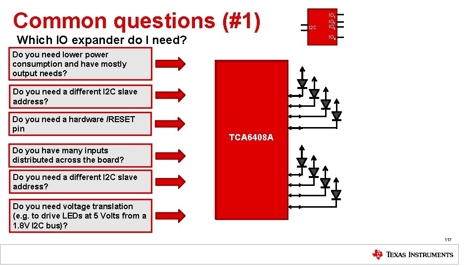
Common questions (#1) Which IO expander do I need? I 2 C IO 1 IO 2 IO 3 ION Do you need lower power consumption and have mostly output needs? Do you need a different I 2 C slave address? Do you need a hardware /RESET pin TCA 9538 TCA 9554 A TCA 9534 TCA 9554 TCA 6408 A Do you have many inputs distributed across the board? Do you need a different I 2 C slave address? Do you need voltage translation (e. g. to drive LEDs at 5 Volts from a 1. 8 V I 2 C bus)? 117