The measurement of the Lorentz angle in the






![X-measurements Dx [mm] We expect displacements linearly proportional to the magnetic field and symmetric X-measurements Dx [mm] We expect displacements linearly proportional to the magnetic field and symmetric](https://slidetodoc.com/presentation_image_h/21e0dde9e3ea3871a2f11dac331c8cc1/image-49.jpg)
![Y-measurements Dx [mm] Displacements are present even with B 0. Also in this case Y-measurements Dx [mm] Displacements are present even with B 0. Also in this case](https://slidetodoc.com/presentation_image_h/21e0dde9e3ea3871a2f11dac331c8cc1/image-50.jpg)








- Slides: 75

The measurement of the Lorentz angle in the BTe. V pixel detectors: the new PCI based DAQ, the setup and the results Lorenzo Uplegger Ph. D. defense Milano 26/01/2004

BTe. V main goals The BTe. V experiment will investigate one of the most fundamental problems of elementary particle physic, the CP violation. Some of the most important aspects of this kind of physics are: • CP violation in b and c quark sector • Measurement of the mixing phenomena of the B 0 s meson • Study of the beauty baryons • Research of new phenomena beyond the Standard Model • Definitively the measurement of the elements of the Cabibbo-Kobayashi-Maskawa matrix

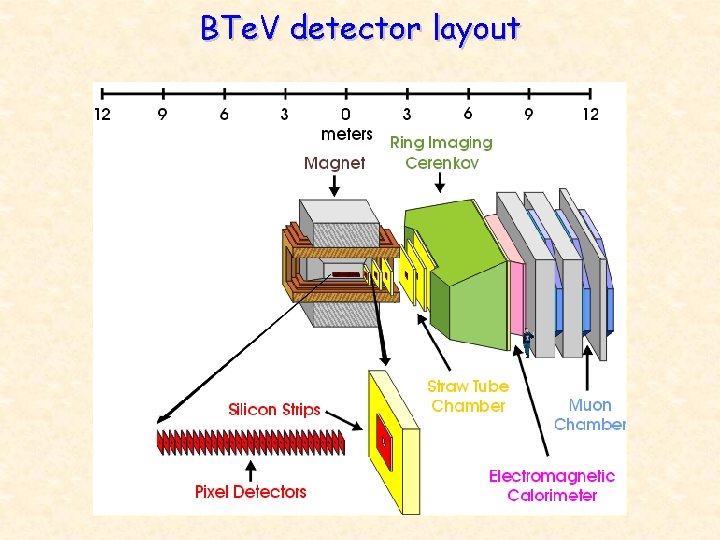
BTe. V detector layout BTe. V main goals

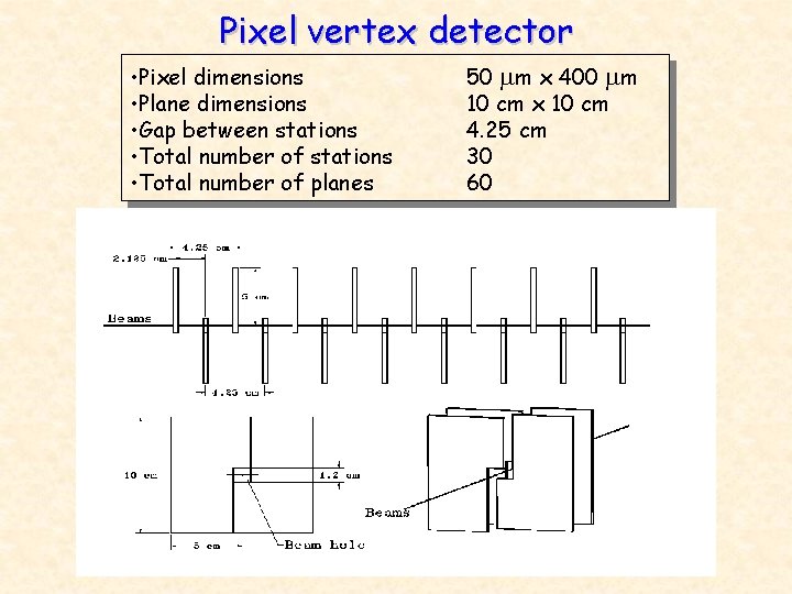
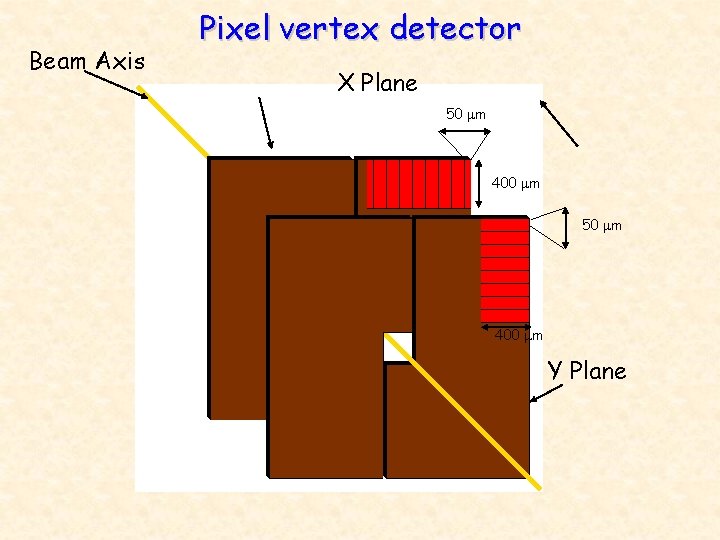
Pixel vertex detector • Pixel dimensions • Plane dimensions • Gap between stations • Total number of planes 50 mm x 400 mm 10 cm x 10 cm 4. 25 cm 30 60

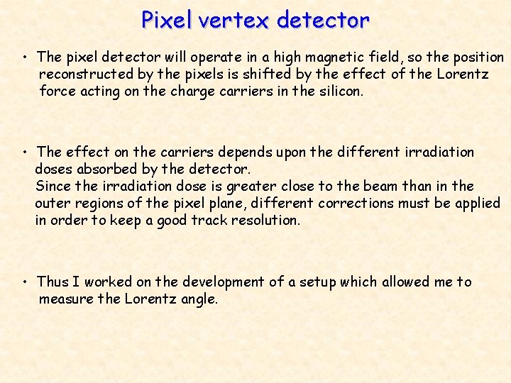
Pixel vertex detector • The pixel detector will operate in a high magnetic field, so the position reconstructed by the pixels is shifted by the effect of the Lorentz force acting on the charge carriers in the silicon. • The effect on the carriers depends upon the different irradiation doses absorbed by the detector. Since the irradiation dose is greater close to the beam than in the outer regions of the pixel plane, different corrections must be applied in order to keep a good track resolution. • Thus I worked on the development of a setup which allowed me to measure the Lorentz angle.

DAQ for pixels • Since the pixel detectors will be tested in a 120 Ge. V beam this year, the work was mainly directed to build a complete read-out system for test-beam studies but flexible enough to allow laboratory bench-test studies and in particular the Lorentz angle measurement. • Furthermore the DAQ system has been designed with enough flexibility to accommodate the m-strip readout chip as well. ( I would recall that my group is responsible for the construction of the m-strip forward tracker ) • I covered many aspects of the design and implementation of this new PCI based DAQ and I will first discuss all the features required by the test-beam needs.

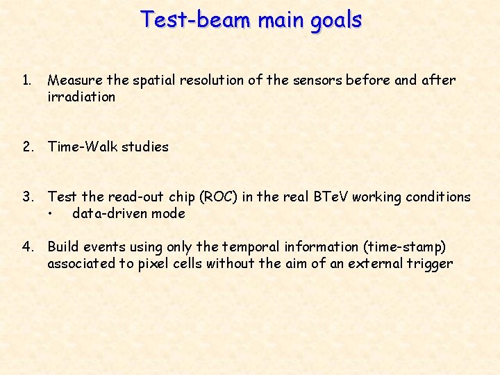
Test-beam main goals 1. Measure the spatial resolution of the sensors before and after irradiation 2. Time-Walk studies 3. Test the read-out chip (ROC) in the real BTe. V working conditions • data-driven mode 4. Build events using only the temporal information (time-stamp) associated to pixel cells without the aim of an external trigger

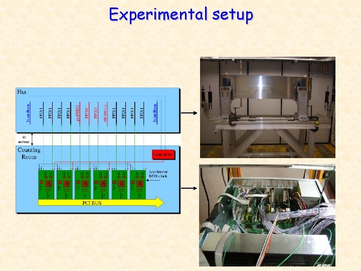
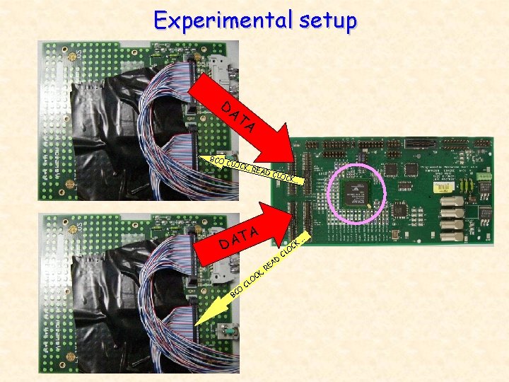
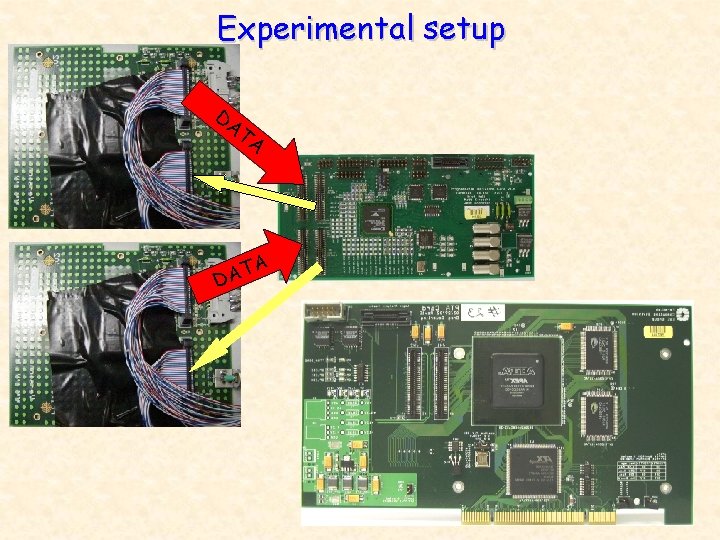
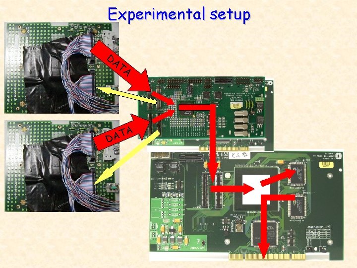
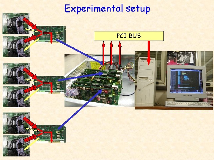
Experimental setup

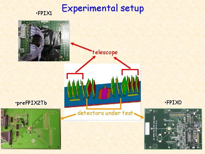
• FPIX 1 Experimental setup telescope • FPIX 0 • pre. FPIX 2 Tb detectors under test

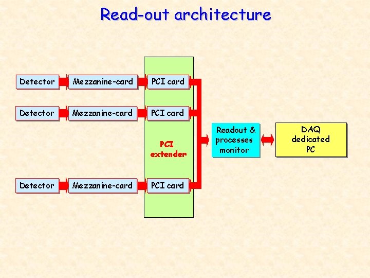
Read-out architecture Detector Mezzanine-card PCI extender Detector Mezzanine-card PCI card Readout & processes monitor DAQ dedicated PC

Experimental setup DA T A BCO CLOC K, RE AD C LOCK … TA A D O BC O CL , CK CK RE AD O CL …

Experimental setup DA TA A T DA

Experimental setup DA TA A T DA

Experimental setup DA TA A AT D DA TA PCI BUS

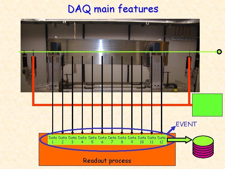
DAQ main features EVENT Data Data Data 1 2 3 4 5 6 7 8 9 10 11 12 Readout process

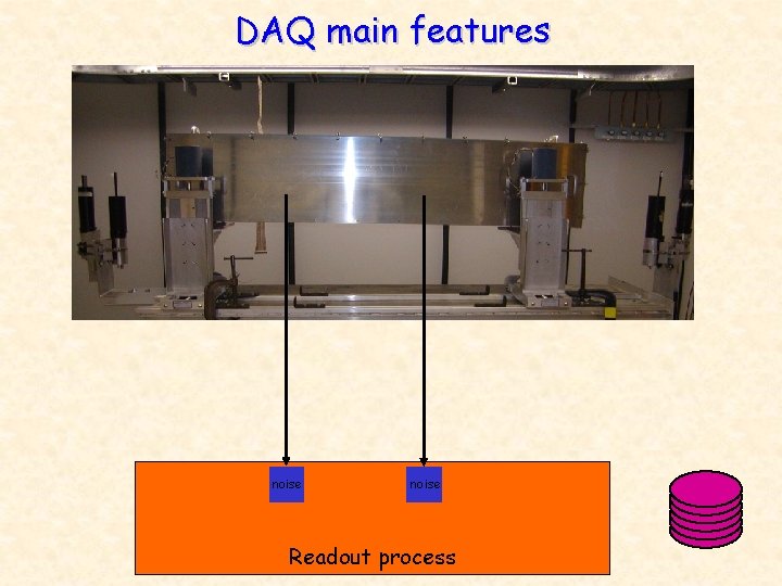
DAQ main features noise Readout process

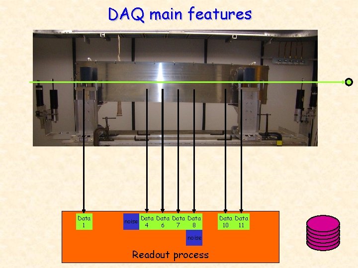
DAQ main features Data 1 noise Data noise 7 8 4 6 noise Readout process Data 10 11

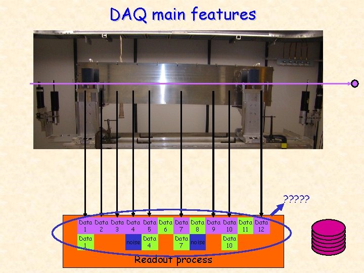
DAQ main features ? ? ? Data Data Data noise 1 2 3 4 5 7 8 9 4 6 Data noise 1 4 7 Readout process Data 10 12 11 Data 10

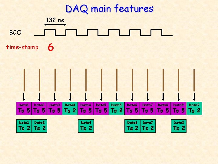
DAQ main features 132 ns BCO time-stamp Data 1 Data 2 4 3 6 2 5 1 Data 3 Data 4 Data 5 Data 6 Data 7 Data 8 Data 9 Ts 5 2 Ts 5 Ts 2 Ts 5 2 Ts 5 2 Ts 2 Data 4 Ts 2 Data 8 Ts 2

DAQ main features The read out system works in absence of an external trigger The data collection from the different pixel detectors is therefore asynchronous The DAQ must assemble the events in asynchronous mode Events are built using the time-stamp information

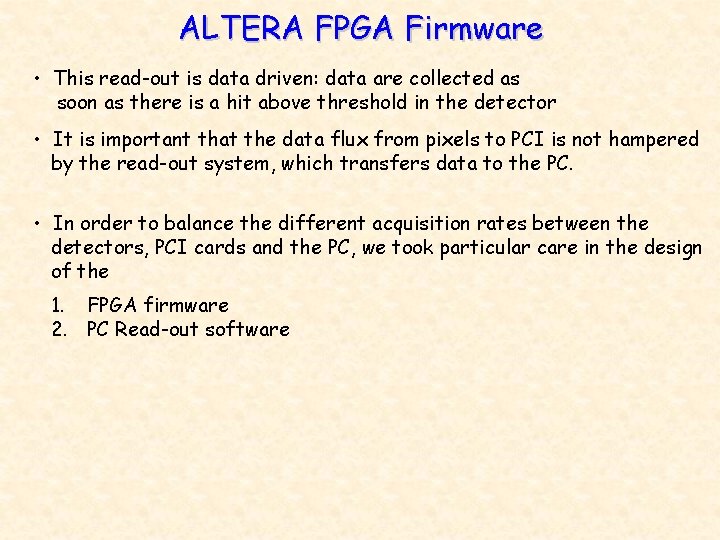
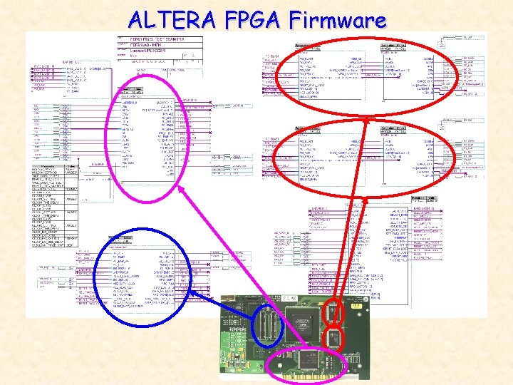
ALTERA FPGA Firmware • This read-out is data driven: data are collected as soon as there is a hit above threshold in the detector • It is important that the data flux from pixels to PCI is not hampered by the read-out system, which transfers data to the PC. • In order to balance the different acquisition rates between the detectors, PCI cards and the PC, we took particular care in the design of the 1. FPGA firmware 2. PC Read-out software

ALTERA FPGA Firmware

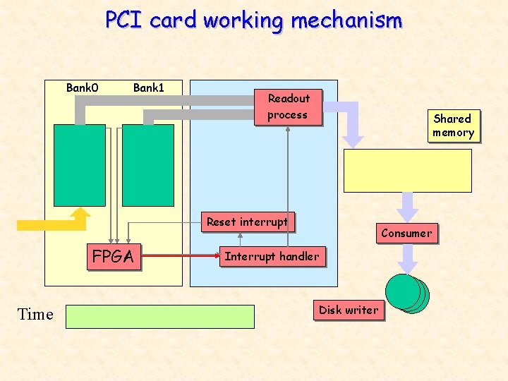
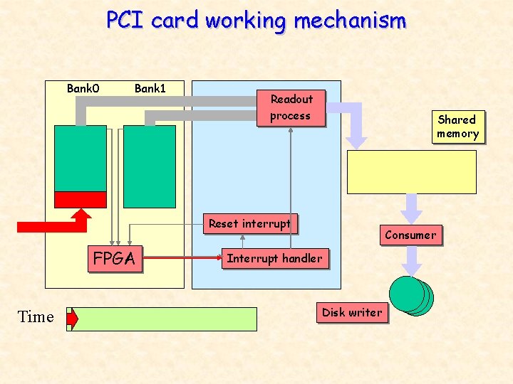
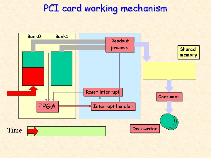
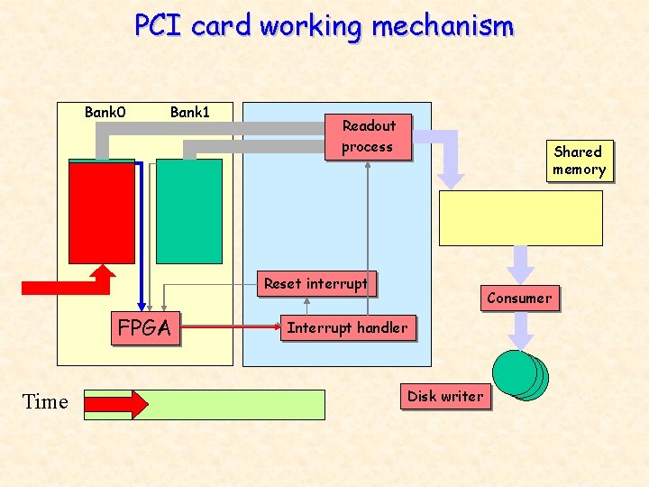
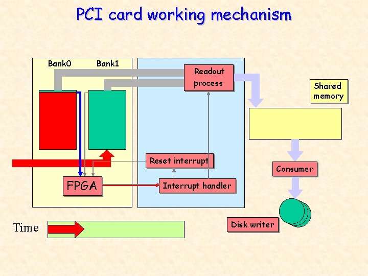
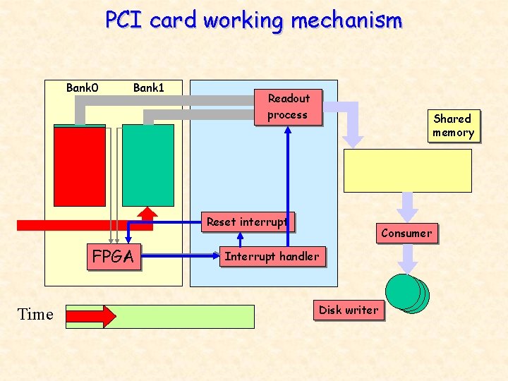
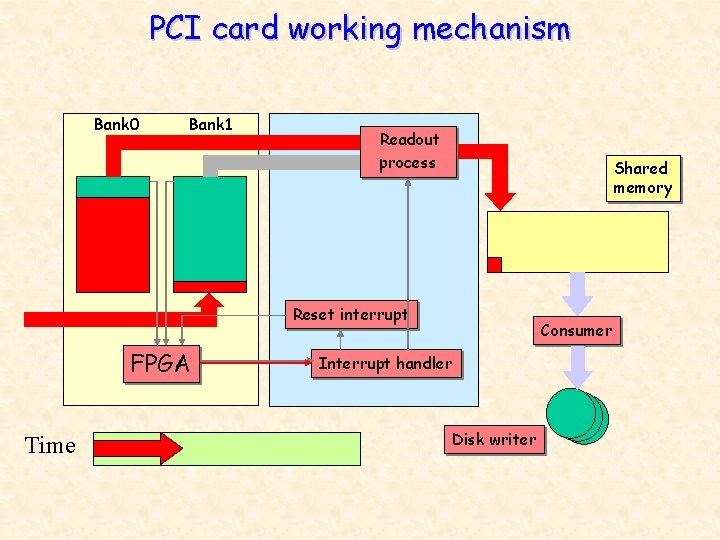
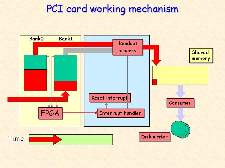
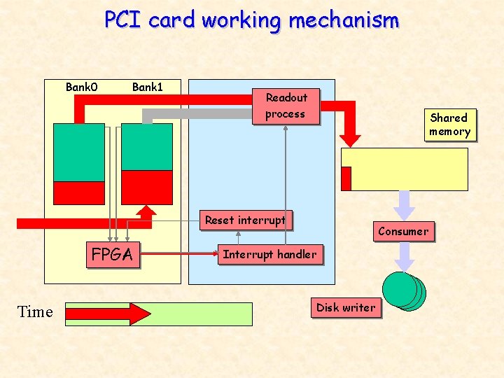
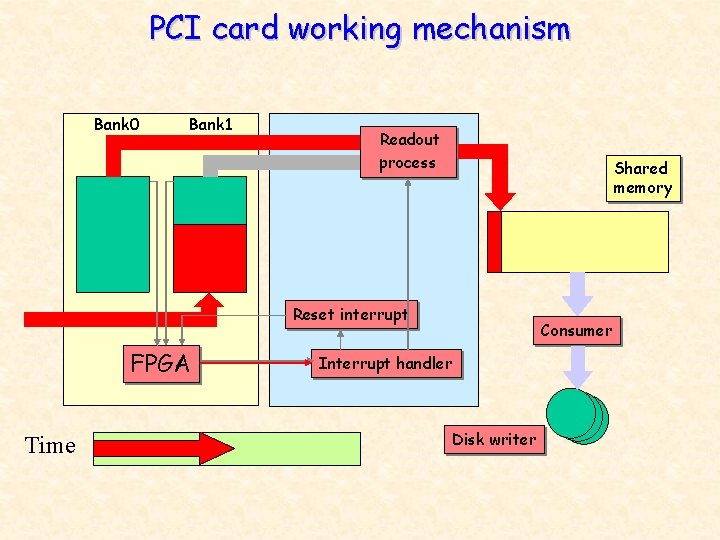
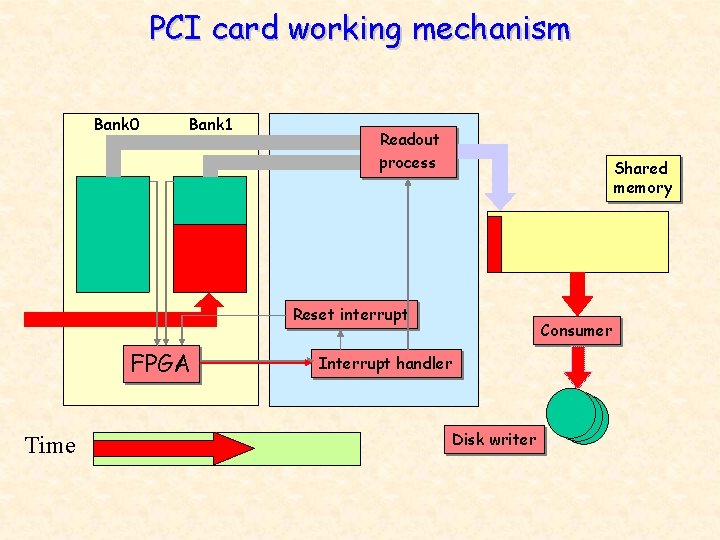
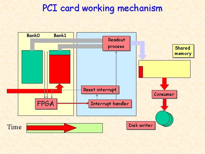
PCI card working mechanism Bank 0 Bank 1 Readout process Shared memory Reset interrupt FPGA Time Consumer Interrupt handler Disk writer

PCI card working mechanism Bank 0 Bank 1 Readout process Shared memory Reset interrupt FPGA Time Consumer Interrupt handler Disk writer

PCI card working mechanism Bank 0 Bank 1 Readout process Shared memory Reset interrupt FPGA Time Consumer Interrupt handler Disk writer

PCI card working mechanism Bank 0 Bank 1 Readout process Shared memory Reset interrupt FPGA Time Consumer Interrupt handler Disk writer

PCI card working mechanism Bank 0 Bank 1 Readout process Shared memory Reset interrupt FPGA Time Consumer Interrupt handler Disk writer

PCI card working mechanism Bank 0 Bank 1 Readout process Shared memory Reset interrupt FPGA Time Consumer Interrupt handler Disk writer

PCI card working mechanism Bank 0 Bank 1 Readout process Shared memory Reset interrupt FPGA Time Consumer Interrupt handler Disk writer

PCI card working mechanism Bank 0 Bank 1 Readout process Shared memory Reset interrupt FPGA Time Consumer Interrupt handler Disk writer

PCI card working mechanism Bank 0 Bank 1 Readout process Shared memory Reset interrupt FPGA Time Consumer Interrupt handler Disk writer

PCI card working mechanism Bank 0 Bank 1 Readout process Shared memory Reset interrupt FPGA Time Consumer Interrupt handler Disk writer

PCI card working mechanism Bank 0 Bank 1 Readout process Shared memory Reset interrupt FPGA Time Consumer Interrupt handler Disk writer

PCI card working mechanism Bank 0 Bank 1 Readout process Shared memory Reset interrupt FPGA Time Consumer Interrupt handler Disk writer

PCI card working mechanism Bank 0 Bank 1 Readout process Shared memory Reset interrupt FPGA Time Consumer Interrupt handler Disk writer

PCI card working mechanism • This process of periodic memory swap and transfer to a shared memory continues indefinetely. • We have several PCI cards playing this swap game in parallel: in order to be able to build events at a later stage, we needed a syncronization mechanism to keep the event builder as simple as possible. • By synchronizing the swapping of all the memories we can build events in a very simple and immediate way.

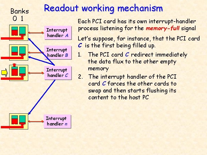
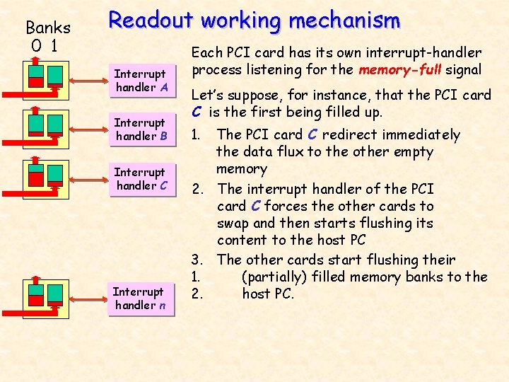
Banks 0 1 Readout working mechanism Interrupt handler A Interrupt handler B Interrupt handler C Interrupt handler n Each PCI card has its own interrupt-handler process listening for the memory-full signal Let’s suppose, for instance, that the PCI card C is the first being filled up. 1. The PCI card C redirect immediately the data flux to the other empty memory 2. The interrupt handler of the PCI card C forces the other cards to swap and then starts flushing its content to the host PC

Banks 0 1 Readout working mechanism Interrupt handler A Interrupt handler B Interrupt handler C Interrupt handler n Each PCI card has its own interrupt-handler process listening for the memory-full signal Let’s suppose, for instance, that the PCI card C is the first being filled up. 1. The PCI card C redirect immediately the data flux to the other empty memory 2. The interrupt handler of the PCI card C forces the other cards to swap and then starts flushing its content to the host PC 3. The other cards start flushing their 1. (partially) filled memory banks to the 2. host PC.

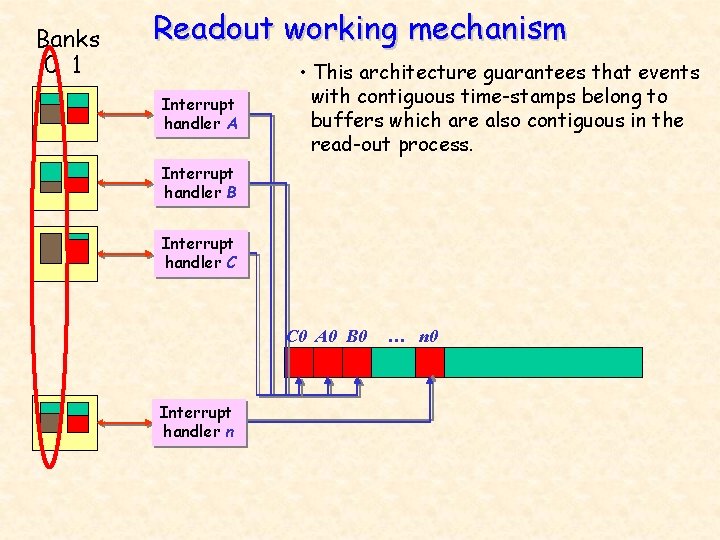
Banks 0 1 Readout working mechanism Interrupt handler A • This architecture guarantees that events with contiguous time-stamps belong to buffers which are also contiguous in the read-out process. Interrupt handler B Interrupt handler C C 0 A 0 B 0 Interrupt handler n … n 0

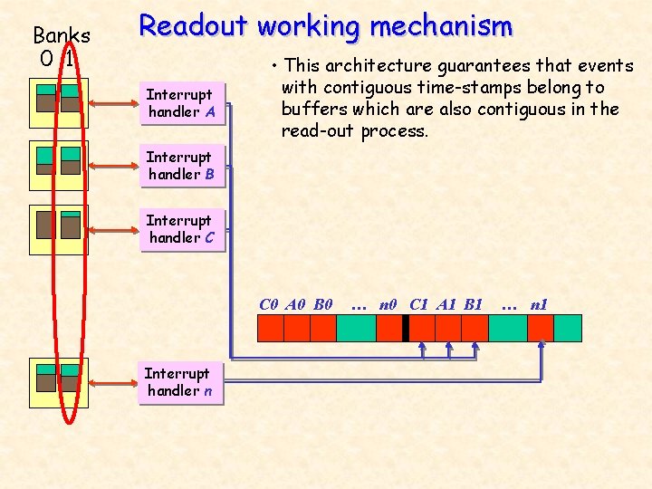
Banks 0 1 Readout working mechanism Interrupt handler A • This architecture guarantees that events with contiguous time-stamps belong to buffers which are also contiguous in the read-out process. Interrupt handler B Interrupt handler C C 0 A 0 B 0 Interrupt handler n … n 0 C 1 A 1 B 1 … n 1

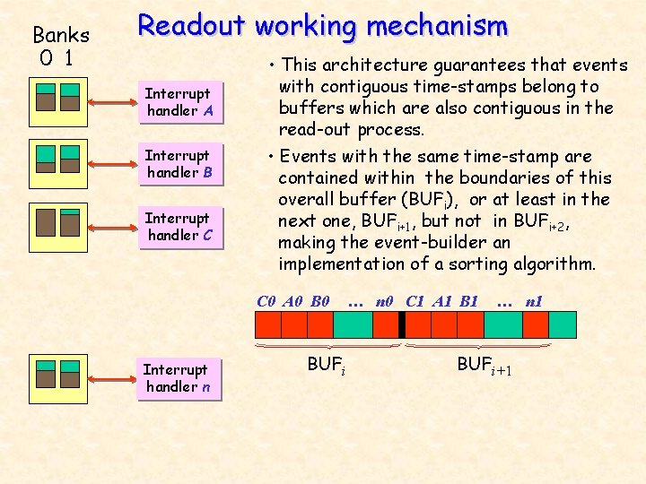
Banks 0 1 Readout working mechanism Interrupt handler A Interrupt handler B Interrupt handler C • This architecture guarantees that events with contiguous time-stamps belong to buffers which are also contiguous in the read-out process. • Events with the same time-stamp are contained within the boundaries of this overall buffer (BUFi), or at least in the next one, BUFi+1, but not in BUFi+2, making the event-builder an implementation of a sorting algorithm. C 0 A 0 B 0 Interrupt handler n BUFi … n 0 C 1 A 1 B 1 … n 1 BUFi+1

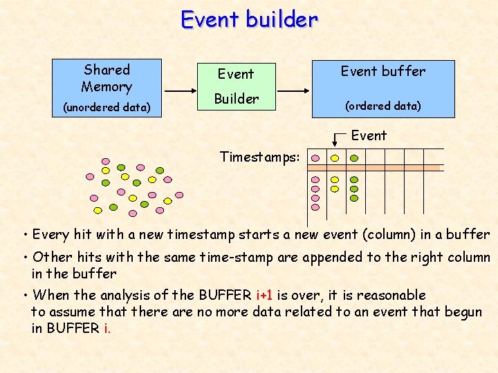
Event builder Shared Memory (unordered data) Event buffer Builder (ordered data) Event Timestamps: • Every hit with a new timestamp starts a new event (column) in a buffer • Other hits with the same time-stamp are appended to the right column in the buffer • When the analysis of the BUFFER i+1 is over, it is reasonable to assume that there are no more data related to an event that begun in BUFFER i.

DAQ conclusion • We built a DAQ system that will be used for the upcoming test-beam • I covered many aspects in the design and implementation of this DAQ: 1. I collaborated on the software development 2. I personally took care of the FPGA programming • I was then able to use this read-out system to measure the Lorentz angle in the silicon pixel detector • I will show now the measurement and the results that I obtained…

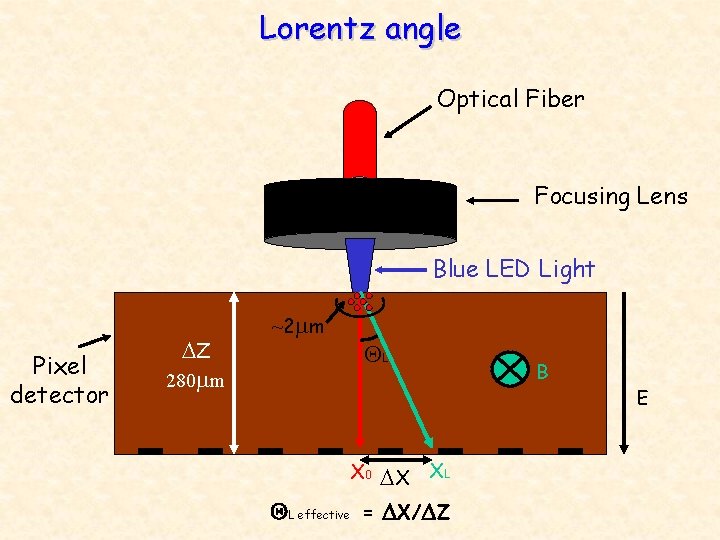
Lorentz angle Optical Fiber Focusing Lens Blue LED Light Pixel detector DZ 280 mm ~2 mm QL D X XL = DX/DZ X 0 QL effective B E

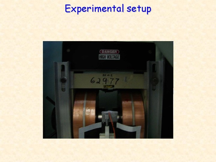
Experimental setup

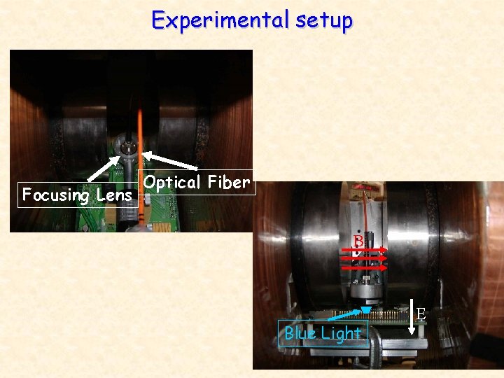
Experimental setup Focusing Lens Optical Fiber B Blue Light E

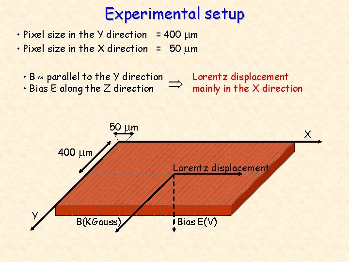
Experimental setup • Pixel size in the Y direction = 400 mm • Pixel size in the X direction = 50 mm • B parallel to the Y direction • Bias E along the Z direction Lorentz displacement mainly in the X direction 50 mm X 400 mm Lorentz displacement Y B(KGauss) Bias E(V)

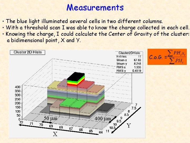
Measurements • The blue light illuminated several cells in two different columns. • With a threshold scan I was able to know the charge collected in each cell. • Knowing the charge, I could calculate the Center of Gravity of the cluster: a bidimensional point, X and Y. C. o. G. = 50 mm 400 mm Y X
![Xmeasurements Dx mm We expect displacements linearly proportional to the magnetic field and symmetric X-measurements Dx [mm] We expect displacements linearly proportional to the magnetic field and symmetric](https://slidetodoc.com/presentation_image_h/21e0dde9e3ea3871a2f11dac331c8cc1/image-49.jpg)
X-measurements Dx [mm] We expect displacements linearly proportional to the magnetic field and symmetric respect to the sign of the B field. Instead here is what I measured B<0 B>0 B KGauss
![Ymeasurements Dx mm Displacements are present even with B 0 Also in this case Y-measurements Dx [mm] Displacements are present even with B 0. Also in this case](https://slidetodoc.com/presentation_image_h/21e0dde9e3ea3871a2f11dac331c8cc1/image-50.jpg)
Y-measurements Dx [mm] Displacements are present even with B 0. Also in this case they are in the same direction reversing the magnetic field. B<0 B>0 B KGauss

Investigating The reason for this effect can be due to: 1. a movement of the apparatus caused by magnetic attraction 2. a residual hysteresis in the ferromagnetic parts of the apparatus 3. a combination of the previous two • I excluded residual hysteresis effects by performing a full set of measurements along a complete hysteresis cycle and checking the reproducibility of the measurements. I didn’t observe any appreciable differences between measurements at the same B value at different points of the hysteresis cycle • So I tried to investigate a possible movement due to the attraction of parts of the apparatus by the magnet

How to measure the mechanical movement? Since the Lorentz displacement is an odd function of the magnetic field, while any movement due to magnetic attraction is an even function of it, by taking the sum of the measured positions at opposite values of the magnetic field one cancel the contribution of the Lorentz effect, and, vice-versa, by taking the difference one cancel the mechanical effect. ( XB +X-B)/2 or ( YB +Y-B)/2 = Mechanical movement ( XB -X-B)/2 or ( YB - Y-B)/2 = Lorentz displacement

Measured mechanical X-movement This movement exists, as shown by the following histograms, and is proportional to the module of the magnetic field as expected, but it should not depend on the value of the BIAS voltage. I checked this by fitting all the movements to a common line (RED) 100 V 150 V 200 V 250 V 300 V 350 V 400 V

Measured mechanical Y-movement Even in this view exists a unique movement that can fit all data with a good c²( c²/d. o. f = 1. 14 ) even if it is not as good as in X 100 V 150 V 200 V 250 V 300 V 350 V 400 V

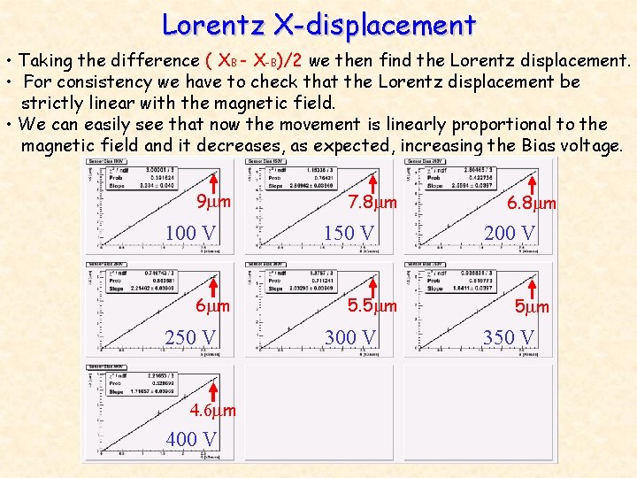
Lorentz X-displacement • Taking the difference ( XB - X-B)/2 we then find the Lorentz displacement. • For consistency we have to check that the Lorentz displacement be strictly linear with the magnetic field. • We can easily see that now the movement is linearly proportional to the magnetic field and it decreases, as expected, increasing the Bias voltage. 9 mm 100 V 6 mm 250 V 4. 6 mm 400 V 7. 8 mm 150 V 5. 5 mm 300 V 6. 8 mm 200 V 5 mm 350 V

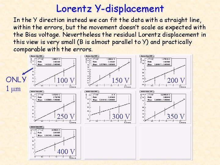
Lorentz Y-displacement In the Y direction instead we can fit the data with a straight line, within the errors, but the movement doesn’t scale as expected with the Bias voltage. Nevertheless the residual Lorentz displacement in this view is very small (B is almost parallel to Y) and practically comparable with the errors. ONLY 1 mm 100 V 150 V 200 V 250 V 300 V 350 V 400 V

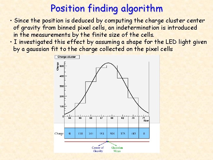
Position finding algorithm • Since the position is deduced by computing the charge cluster center of gravity from binned pixel cells, an indetermination is introduced in the measurements by the finite size of the cells. • I investigated this effect by assuming a shape for the LED light given by a gaussian fit to the charge collected on the pixel cells

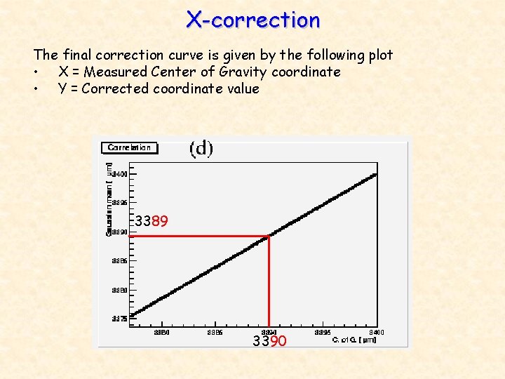
X-correction The final correction curve is given by the following plot • X = Measured Center of Gravity coordinate • Y = Corrected coordinate value 3389 3390

X-corrected mechanical movement The correction is really tiny for the mechanical movement. 100 V 150 V 200 V 250 V 300 V 350 V 400 V

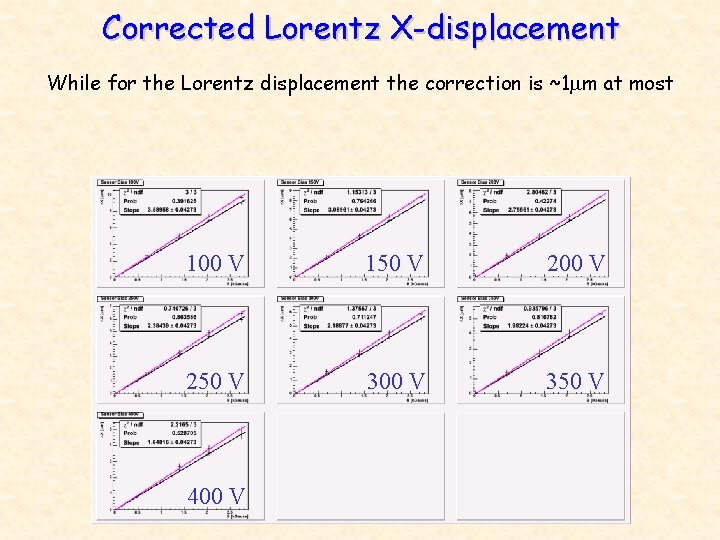
Corrected Lorentz X-displacement While for the Lorentz displacement the correction is ~1 mm at most 100 V 150 V 200 V 250 V 300 V 350 V 400 V

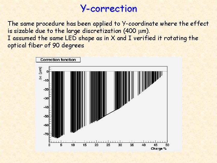
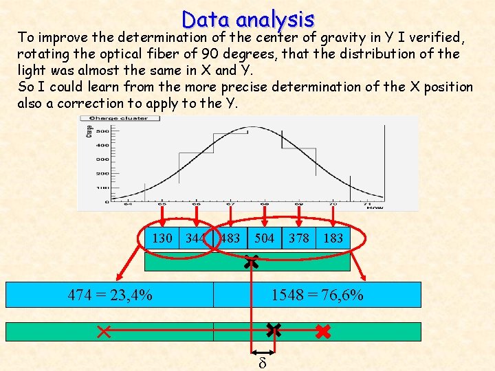
Y-correction The same procedure has been applied to Y-coordinate where the effect is sizable due to the large discretization (400 mm). I assumed the same LED shape as in X and I verified it rotating the optical fiber of 90 degrees

Corrected Y-mechanical movement 100 V 150 V 200 V 250 V 300 V 350 V 400 V

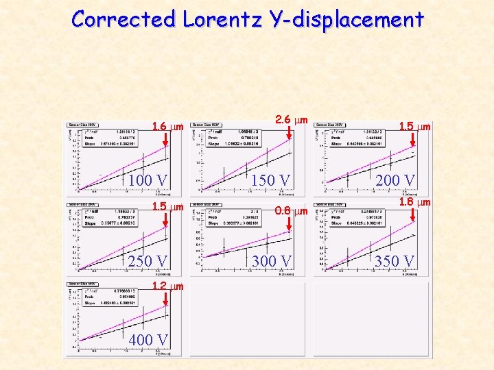
Corrected Lorentz Y-displacement 1. 6 mm 100 V 1. 5 mm 250 V 1. 2 mm 400 V 2. 6 mm 150 V 0. 8 mm 300 V 1. 5 mm 200 V 1. 8 mm 350 V

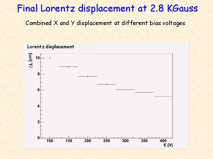
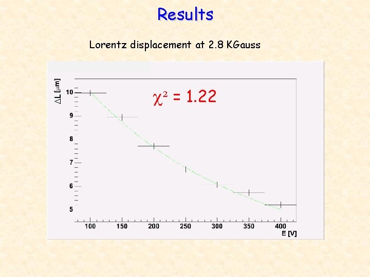
Final Lorentz displacement at 2. 8 KGauss Combined X and Y displacement at different bias voltages DL Lorentz displacement

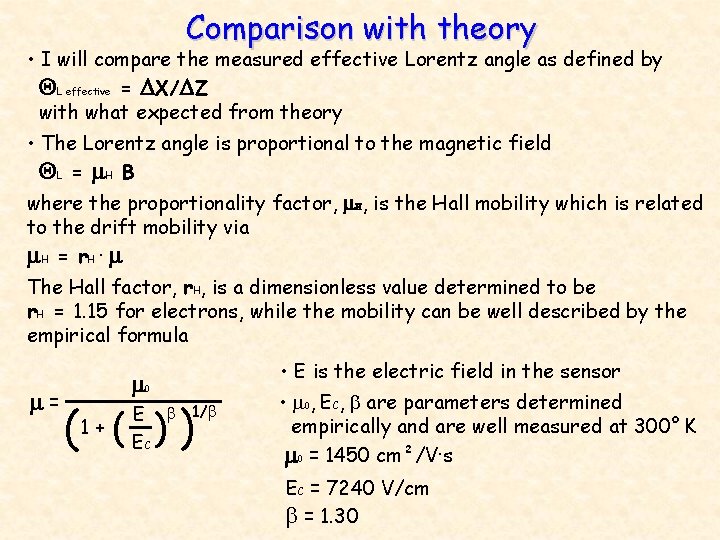
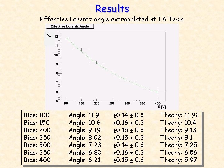
Comparison with theory • I will compare the measured effective Lorentz angle as defined by QL effective = DX/DZ with what expected from theory • The Lorentz angle is proportional to the magnetic field QL = m. H B where the proportionality factor, m. H, is the Hall mobility which is related to the drift mobility via m. H = r H · m The Hall factor, r. H, is a dimensionless value determined to be r. H = 1. 15 for electrons, while the mobility can be well described by the empirical formula m= m 0 (1 + ( ) ) E b EC 1/b • E is the electric field in the sensor • m 0, EC, b are parameters determined empirically and are well measured at 300° K m 0 = 1450 cm²/V·s EC = 7240 V/cm b = 1. 30

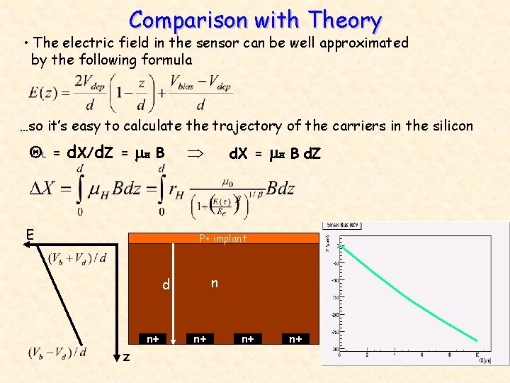
Comparison with Theory • The electric field in the sensor can be well approximated by the following formula …so it’s easy to calculate the trajectory of the carriers in the silicon QL = d. X/d. Z = m. H B E d. X = m. H B d. Z P+ implant n d z n+ n+

Results DL Lorentz displacement at 2. 8 KGauss c² = 1. 22

Results Effective Lorentz angle extrapolated at 1. 6 Tesla QL Bias: 100 Bias: 150 Bias: 200 Bias: 250 Bias: 300 Bias: 350 Bias: 400 Angle: 11. 9 Angle: 10. 6 Angle: 9. 19 Angle: 8. 02 Angle: 7. 23 Angle: 6. 83 Angle: 6. 21 ± 0. 14 ± 0. 3 ± 0. 16 ± 0. 3 ± 0. 15 ± 0. 3 Theory: 11. 92 Theory: 10. 4 Theory: 9. 13 Theory: 8. 1 Theory: 7. 25 Theory: 6. 56 Theory: 5. 97

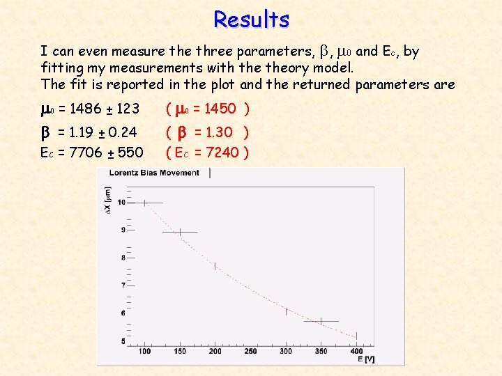
Results I can even measure three parameters, b, m 0 and Ec, by fitting my measurements with theory model. The fit is reported in the plot and the returned parameters are m 0 = 1486 ± 123 b = 1. 19 ± 0. 24 EC = 7706 ± 550 ( m 0 = 1450 ) ( b = 1. 30 ) ( EC = 7240 )

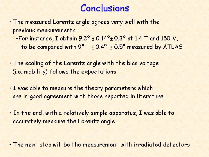
Conclusions • The measured Lorentz angle agrees very well with the previous measurements. -For instance, I obtain 9. 3º ± 0. 14º± 0. 3º at 1. 4 T and 150 V, to be compared with 9º ± 0. 4º ± 0. 5º measured by ATLAS • The scaling of the Lorentz angle with the bias voltage (i. e. mobility) follows the expectations • I was able to measure theory parameters which are in good agreement with those reported in literature. • In the end, with a relatively simple apparatus, I was able to accurately measure the Lorentz angle. • The next step will be the measurement with irradiated detectors

BACK UP SLIDES

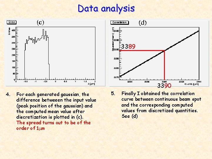
Data analysis In order to improve the determination of the X displacement I add a correction in the X-direction performing a Monte. Carlo simulation that takes into account this effect. 1. I generated a sample of 10, 000 gaussians with fixed width and amplitude taken from the data sample shown in figure (b) (a) 2. The mean value of these gaussians has been plotted in (a) 3. For each chosen gaussian, the shape as been superimposed on a grid of pixels at fixed positions, and the fraction of gaussian area overlapping each bin has been computed. The mean values of these redistributed charges (C. o. G) have been computed and plotted in (b)

Data analysis 3389 3390 4. For each generated gaussian, the difference betweeen the input value (peak position of the gaussian) and the computed mean value after discretization is plotted in (c). The spread turns out to be of the order of 1 mm 5. Finally I obtained the correlation curve between continuous beam spot and the corresponding computed values from discretized quantities. See (d)

Data analysis To improve the determination of the center of gravity in Y I verified, rotating the optical fiber of 90 degrees, that the distribution of the light was almost the same in X and Y. So I could learn from the more precise determination of the X position also a correction to apply to the Y. 130 344 483 504 378 183 474 = 23, 4% 1548 = 76, 6% d

Beam Axis Pixel vertex detector X Plane 50 mm 400 mm Y Plane